background image

-  13  -

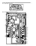
IC  BLOCK  DIAGRAM & DESCRIPTION

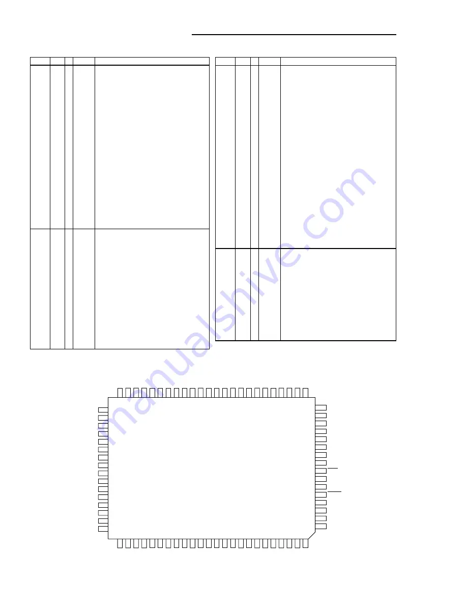
IC601  IC LC72338-9C41-E (Single-Chip PLL + Controller)

Pin name Pin No. I/O I/O Format

Functions

S21/PF0
S22/PF1/SCK1
S23/PF2/SO1
S24/PF3/SI1

S29/PN0/BEEP
S30/PN1
S31/PN2
S32/PN3

35 
34 
33 
32

26 
25 
24 
23

I/O

O

LCD driver segment output, general-porpose input/output and
serial I/O ports.
The PF0 to 3 inputs are in the Schmidt format.
The IOS instruction is used to switch between the LCD driver
segment output, general-purpose I/O, and serial I/O functions, and 
to switch between input and output of the general-purpose input 
port function.
  •  For use as segment output
    These pins can be set in 4 bits units. The IOS instruction with 
    Pn=OEH specifies segment output use in bit units.
      b0=S21 to 24/ PF0 to 3  

0 • • • Segment output


1 • • • PE0 to 3

  •  For use as general-purpose input /output port
    These pins can be set to input /output in bit units. (1 bit I/O)
      b1=SI/O   1 

0 • • • Genetal-purpose port


1 • • • SI/O port

    Input /output is specified with the IOS instruction in bit units.
      PF • • • Pn=5  0 • • • Input


1 • • • Output

  •  For use as serial I/O port
    The serial I/O port function is specified with the IOS instruction 
    (Pn=0). The contents of the serial I/O data buffer can be saved 
    and loaded with the INR and OUTR instructions.
      *Pin setup states when used as a serial I/O port
      PF0 • • • General-purpose input /output
      PF1 • • • SCK1 output in internal clock mode


SCK1 output in external clock mode

      PF2 • • • SO1 output
      PF3 • • • SI1 input
In CLOCK STOP mode, if this port is used as a general-purpose
I/O port or as a serial I/O port, the pins go to the input disabled 
high-impedance state. If used for segment output, the pins are 
fixed at the low level. The segment output port function is selected 
after a power-on reset.

Segment output/general-porpose input port 1/ BEEP tone output 
pins. The IOS instruction is used to switch between the segment 
output port and the PN0 to 3 functions. The BEEP instruction 
switches between the general-purpose output port and BEEP tone 
function.
  •  For use as segment output
    These pins can be set in 3 bits units.  The IOS instruction with 
    Pn=OEH specifies segment output use in bit units.
      b2=S29 to 32/ PN0 to 3  

0 • • • Segment output


1 • • • PN0 to 3

  •  For use as general-purpose output.
    The general-porpose output port function is selected with the 
    BEEP instruction (b3=0).
    PN1 to 3 are dedicated general-purpose output function pins.
  •  For use as BEEP output pin
    The BEEP instruction with b3=1 sets the BEEP output. 
    The BEEP instruction bit b0,b1 and b2 sets the frequency.
    When this is set as the BEEP port, executing an output
    instruction will rewrite the internal latch data but has no 
    influence on the output.
These pins go to the output high-impedance state in clock stop 
mode. If used for segment output, the pins are fixed at the low level. 
These pins go to the output high-impedance state during the 
power-on reset and hold that state until an output instruction is 
executed.

CMOS

three
value

output

and

push-pull

CMOS

three
value

output

and

push-pull

Pin name Pin No. I/O I/O Format

Functions

S17/PE0
S18/PE1/SCK2
S19/PE2/SO2
S20/PE3/SI2

S25/PM0
S26/PM1
S27/PM2
S28/PM3

39 
38 
37 
36

30 
29 
28 
27

I/O

I/O

LCD driver segment output, general-porpose input/output and
serial I/O ports
The IOS instruction is used to switch between the LCD driver
segment output, general-purpose I/O, and serial I/O functions,
and to switch between input and output of the general-purpose
input port function.
  •  For use as segment output
    These pins can be set in bit units.
    The IOS instruction with Pn=ODH specifies segment output
    use in bit units.
      b0=S17/PE0  0 • • • Segment output
      b1=S18/PE1  1 • • • PE0 to 3 output
      b2=S19/PE2
      b3=S20/PE3
  •  For use as general-purpose input /output port
    These pins can be set for input /output in bit units.
    (1 bit I/O)
      b2=SI/O2 

0 • • • Genetal-purpose port


1 • • • SI/O port

    Input /output is specified with the IOS instruction in bit units.
      PE • • • Pn=4  0 • • • Input


1 • • • Output

  •  For serial I/O port
    The serial I/O port function is specified with the IOS instruction 
    (Pn=0).
    The contents of the serial I/O data buffer can be saved and 
    loaded with the INR and OUTR instructions.
      *Pin setup states when used as a serial I/O port
      PE0 • • • General-purpose input /output
      PE1 • • • SCK2 output in internal clock mode


SCK2 output in external clock mode

      PE2 • • • SO2 output
      PE3 • • • SI2 input
In CLOCK STOP mode, if this port is used as a general-purpose
I/O port or as a serial I/O port, the pins go to the input disabled 
high-impedance state. If used for segment output, the pins fixed at 
the low level. The segment output port function is selected after a 
power-on reset.


LCD driver segment output, general-porpose input /output ports.
The IOS instruction is used to switch between the LCD driver
segment output, general-purpose I/O port, and serial I/O to switch 
between input and output of the general-purpose input /output 
port function.
  •  For use as segment output
    These pins can be set in 4 bits units. The IOS instruction with 
    Pn=OEH specifies segment output use in bit units.
      b0=S25 to 28/PM0 to 3  

0 • • • Segment output


1 • • • PM0 to 3

  •  For use as general-purpose input /output port
    These pins can be set for input /output in bit units.
    Input /output is specified with the IOS instruction in bit units.
      PM • • • Pn=OCH   


0 • • • Input


1 • • • Output

In CLOCK STOP mode, if this port is used as a general-purpose
I/O port, the pins go to the input disabled high-impedance state. If 
used for segment output, the pins are fixed at the low level. The 
segment output port function is selected after a power-on reset.

CMOS

three
value

output

and

push-pull

CMOS

three
value

output

and

push-pull

XIN

TEST2

SI0/PG3

SO0/PG2

SCK0/PG1

PG0

PC3 

PC2

PC1 

PC0

PB3

PB2 

PB1 

PB0 

PA
3

PA
2


PA
1


PA
0


PK3 

PK2 

INT1/PK1

INT0/PK0 

PN3/S32

PN2/S31

10 

11 

12 

13 

14 

15 

16 

17 

18 

19 

20 

21 

22 

23 

24

64 

63 

62 

61 

60 

59 

58 

57 

56 

55 

54 

53 

52 

51 

50 

49 

48 

47 

46 

45 

44 

43 

42 

41

PJ0/D

A

C

PJ1/D

A

C

1

PJ2/D

A

C

PJ3/D

A

C

Vdd1

Vdd2 

COM1 

COM2 

COM3 

S1

S2 

S3 

S4 

S5 

S6 

S7 

S8 

S9 

S10 

S11 

S12 

S13 

S14 

S15

25

26

27

28

29

30

31

32

33

34

35

36

37

38

39

40

80

79

78

77

76

75

74

73

72

71

70

69

68

67

66

65

PN1/S30

BEEP/PN0/S29

PM3/S28

PM2/S27

PM1/S26

PM0/S25

[Vpp]Vdd

SI1/PF3/S24

SO1/PF2/S23

SCK1/PF1/S22

PF0/S21

SI2/PE3/S20

SO2/PE2/S19

SCK2/PE1/S18

PE0/S17

S16

XOUT

TEST1

E02

E01

VSS

AMIN

FMIN

Vdd

SNS

LCTR

HCTR

HOLD

PH0/ADI0

PH1/ADI1 

PH2/ADI2 

PH3/ADI3

Summary of Contents for DC-DA1100 (XE)

Page 1: ...165 104 01 Contents Laser beam safety precaution 1 Tape adjustments 1 Tuner adjustments 2 CD pick up maintenance 2 Exploded view Cabinet Chassis 3 Parts list 4 Exploded view Parts list Tape mechanism 7 IC block diagram description 7 LCD display description 14 Wiring connection 15 CD Schematic diagram FRONT 16 CD 18 TUNER 22 AMPLIFIER 26 Wiring diagram FRONT CD 20 TUNER 24 AMPLIFIER 28 POWER TRANSF...

Page 2: ... 70gr cm 1 0 6 0gr cm 80 gr or more F FWD REW 55 gr or more CAUTION INVISIBLE LASER RADIATION WHEN OPEN AND INTERLOCKS DEFEATED AVOID EXPOSURE TO BEAM ADVARSEL USYNLIG LASER STRÅLING VED ÅBNING NÅR SIKKERHEDSAFBRYDERE ER UDE AF FUNKTION UNDGÅ UDS ÆTTELSE FOR STRÅLING VARNING OSYNLIG LASER STRÅLNING NÄR DENNA DEL ÄR ÖPPNAD OCH SPÄRR ÄR URKOPPLAD STRÅLEN ÄR FARLIG VORSICHT UNSICHTBARE LASERSTRAHLUNG...

Page 3: ...4 TP15 T2001 CT211 IC211 T2002 Antenna 75Ω unbalanced direct Modulation 1 kHz Dev 22 5kHz MONO 22 5kHz MAIN 6 75kHz PILOT RF Level dBuV EMF Output Level about 30mV at TP13 TP14 TP15 Anntena IRE Loop SG Moduration 1kHz 30 RF Level dBuV EMF Output Level about 30mV at TP13 TP14 TP15 CD PICK UP MAINTENANCE About pick up Optical lens Cleaning Clean a lens with swab of the cotton which moistened it with...

Page 4: ...29 8 6 7 11 22 2 13 14 15 17 18 16 3 4 5 1 23 53 21 22 22 24 Y03 Y01 Y02 Y05 Y05 Y04 Y04 Y05 Y06 Y07 55 56 51 52 54 Y11 Y11 Y12 Y14 Y13 Y15 Y15 Y16 Y16 Y19 Y19 Y21 Y20 Y20 Y18 Y18 Y17 Y13 Y08 Y09 Y10 Y10 Y10 Y09 Y07 Y07 71 72 73 74 75 76 57 58 This is a basic exploded view ...

Page 5: ...NG DECK MECHA 20 614 308 0534 SPRING PLATE REC 21 614 310 3899 SPACER MECHA CD DA11 22 614 325 6014 ASSY MECHA DA11T3CN SASH 23 614 307 2072 COVER PICK UP 24 614 322 2132 ASSY GEAR LID CD 25 614 329 2357 MOUNTING CD 26 614 303 0263 LATCH PUSH CD DOOR LOCKING 27 614 307 8821 PULLEY 28 614 303 0256 LATCH MAGNET 29 614 329 2456 SPRING DOOR CD 30 614 329 2333 LID CD 31 614 329 2234 DEC WINDOW CD 32 61...

Page 6: ...U K L2204 645 037 2377 TRANS ANT 796KHZ or 645 058 8792 TRANS ANT 796KHZ L2205 645 040 2739 TRANS OSC 796KHZ or 645 058 8822 TRANS OSC 796KHZ Q2001 405 151 4301 TR KTC3195 Y or 405 151 4806 TR KTC3195 O D6901 407 012 4406 DIODE 1SS133 D6902 407 012 4406 DIODE 1SS133 D6951 407 235 7406 LED LT7V34 81 URC1 LCD LIGHT D6952 407 235 7406 LED LT7V34 81 URC1 FRONT LIGHT IC601 410 517 4208 IC LC72338 9C41 ...

Page 7: ...FILTER 450KHZ T2002 645 039 9923 TRANS IF 10 7MHZ or 645 040 9981 TRANS IF 10 7MHZ or 645 060 4089 TRANS IF 10 7MHZ XF210 645 059 0047 FILTER BP or 645 026 2975 FILTER BP 108MHZ or 614 252 1045 FILTER LC XF211 645 054 1223 CERAMIC FILTER 10 70MHZ or 645 010 7665 CERAMIC FILTER 10 70MHZ or 614 240 2917 FILTER CERAM XF212 645 054 1223 CERAMIC FILTER 10 70MHZ or 645 010 7665 CERAMIC FILTER 10 70MHZ o...

Page 8: ... 2 59 64 11 32 33 62 8 VDD3V 63 23 Slice level Control Subcode Separation QCRC Syncrnous Detection EFM Demodulation VCO Clock Oscillator Clock Control Crystal Oscillator System Generator RAM Address Generatorl Digital Output General PurposePort Digital Attenuator 8X Over Sampling Digital Filter Interpolalation Mute C1 C2 Error Detection Correction Flag Processing 1bit DAC L P F CLV Digital Servo M...

Page 9: ...nected to 0V External VCO control phase comparator output pin PDO output current adjustment resistor connection pin Internal VCO power supply pin VCO frequency range adjustment Digital system ground pin Must be connected to 0V Slice level control EFM signal output pin EFM signal input pin Test input pin A pull down resistor is built in Must be connected to 0V Disk motor control output Can be set t...

Page 10: ...4 3 2 1 Vcc1 LDS LDD BH1 PH1 LF2 VR REF1 Vcc2 DRF CE DAT CL CLK DEF NC TBC FSC DGND SLI SLC RFS RFSM CV CV SLOF HFL TES TOFF TGL JP JP SL SL SLD SLEQ SPD SP SPG SPI SP AGND FE FE FA FA FD FD TO JP TD TD TA TH SCH TESI TE TE TB F E FIN1 FIN2 APC RF DET REF VCA I V BAL VCA INTER FACE SLC RF Amp TE T SERVO T LOGIC F SERVO F LOGICK SPINDLE SERVO SLED SERVO IC101 LA9242M MPB Servo Processing Signal for...

Page 11: ...9 18 17 16 15 14 13 IC211 LA1844ML Tuner System CONTROL CIRCUIT LOGIC CIRCUIT CCB INTERFACE CONTROL CIRCUIT 15 14 16 17 18 19 20 21 22 24 25 26 23 10 9 7 6 5 8 11 L4 L3 L2 L1 NC NC R1 R2 R3 R4 RSELO RIN RTRE RBASS1 RBASS2 ROUT LSELO LIN LTRE LBASS1 LBASS2 LOUT TEST VSS CE DI CL VDD Vref NC 12 13 1 2 30 29 28 27 4 3 LVref RVref IC411 LC75342M Function SW Electric Volume 2 Band Equalizer IC412 TA822...

Page 12: ... 70 71 AMIN SNS HOLD VDD VSS HCTR LCTR 69 79 2 18 17 16 15 14 13 12 11 10 9 8 7 TEST1 TEST2 PA0 PA1 PA2 PA3 PB0 PB1 PB2 PB3 PC0 PC1 PC2 PC3 6 5 4 3 PG0 SCK0 PG1 SO0 PG2 SI0 PG3 LATCH BUS DRIV LATCH BUS DRIV LATCH BUS DRIV SIO BUS DRIV 1 2 V DET SNSFF 1 16 1 17 PROGRAMMABLE DIVIDER LATCH UNIVERSAL COUNTER 20bits RAM 512 x 4bits ROM 8K x 16bits ADDRESS DECODER BUS DRIVER INSTRUC TION DECODER ADDRESS...

Page 13: ...function between universal counter input and general puropse input Frequency measurement The universal counter function is selected by an IOS instruction with Pn 3 and b3 0 LCTR frequency measure ment mode is set up by a UCS instruction with b3 0 and b2 1 and counting is started with a UCC instruction after the count time is selected The CNTEND flag is set when the count completes To operate this ...

Page 14: ... PE2 SO2 S20 PE3 SI2 S25 PM0 S26 PM1 S27 PM2 S28 PM3 39 38 37 36 30 29 28 27 I O I O LCD driver segment output general porpose input output and serial I O ports The IOS instruction is used to switch between the LCD driver segment output general purpose I O and serial I O functions and to switch between input and output of the general purpose input port function For use as segment output These pins...

Page 15: ... S16 S17 S18 S19 S20 S21 S22 S23 S24 S25 COM1 4M 3A 3B 3M T2 T9 T8 2A 2B 2h 1A 1B 1h SURR COM2 4C 3F 3G 3C T4 T3 4h 2F 2G 2C 1F 1G 1C SLEEP COM3 4K 3E 3D 3K T7 3h 2E 2D MONO 1E 1D 1K AM 1 A G K K K M M B F D C E 1 1h 3h 4h 2h T1 T9 T2 T4 T6 T7 T3 T5 T8 2 3 4 5 6 7 28 LCD60 IC BLOCK DIAGRAM DESCRIPTION 28 27 26 25 24 23 22 21 20 19 18 17 16 15 1 2 3 4 5 6 7 8 9 10 11 12 13 14 Vcc Vcc DRIVER MUTE D ...

Page 16: ... LCD60 CN601 14P CN202 16P CN204 2P CN604 2P CN201 CN122 8P CD MECHANISM CN111 16P 16P CN113 6P 6P CN441 2P CN490 8P CN491 14P CN421 PHONES CN402 2P CN401 2P CN406 4P CN405 4P FU401 T2 5A L 250V AMPLIFIER P W B TUNER P W B AM LOOP ANT CN455 2P P T AC IN CN452 BL CN451 BW MOTOR SWITCH R P HEAD RED ORANGE YELLOW BROWN M TAPE DECK MECHANISM CN203 1P FM ANT ...

Page 17: ... 470 10K 25 26 27 28 29 30 31 32 33 34 35 36 37 38 39 40 80 79 78 77 76 75 74 73 72 71 70 69 68 67 66 65 1 2 3 4 5 6 7 8 9 10 11 12 13 14 15 16 17 18 19 20 21 22 23 24 64 63 62 61 60 59 58 57 56 55 54 53 52 51 50 49 48 47 46 45 44 43 42 41 1 2 3 5 4 1 2 3 4 5 6 7 8 9 10 11 12 13 14 15 16 17 18 19 20 21 22 23 24 25 26 27 28 2 1 KEY2 GND CN604 1 2 3 1 2 3 4 5 6 7 8 9 10 11 12 13 14 1 2 3 4 5 6 7 8 9...

Page 18: ...220P 100 0 1 1SS133 1SS133 1SS133 330K 100P 0 022 100P 16 15 14 13 12 11 10 9 8 7 6 5 4 3 2 1 32 31 30 29 28 27 26 25 24 23 22 21 20 19 18 17 33 34 35 36 37 38 39 40 41 42 43 44 45 46 47 48 64 63 62 61 60 59 58 57 56 55 54 53 52 51 50 49 48 47 46 45 44 43 42 41 40 39 38 37 36 35 34 33 16 15 14 13 12 11 10 9 8 7 6 5 4 3 2 1 49 50 51 52 53 54 55 56 57 58 59 60 61 62 63 64 32 31 30 29 28 27 26 25 24 ...

Page 19: ...LIM SW J1308 D1401 D1402 D1403 J1119 J1317 J1318 C1457 J1206 J1300 J1212 J1104 J1306 J1108 C1783 J1100 J1207 C1476 C1478 D1410 J1120 J1304 J1322 J1114 J1117 J1113 J1116 C1492 J1107 IC102 IC101 J1103 X1451 J1105 J1215 R6201 R6201 R6112 R6112 C6910 C6910 C6501 C6501 C6203 C6203 C1772 C1772 C1782 C1782 C1475 C1475 C1404 C1404 R1773 R1773 R1465 R1465 R6201 C6201 C6903 R6905 C6901 C6901 C6204 C6204 R61...

Page 20: ...2 0 47 50 10K 0 01 0 01 KRA107M 3 9K 0 01 10 25 10K 2 7K 100 10 0 47 50 1 50 0 047 LA1844ML 820K KRA107M 27K 100 1000P 18K 0 022 0 022 0 033 680P 0 022 0 022 4 7 50 22 25 1SS133 2 2 50 2 2 50 68K KRC107M 2 2K 100 10 15K 0 022 0 1 1000P 1P KRC107M 10K 15K 0 022 KTC3195 330K 4 7K 0 022 1 0K SVC211 B C SVC211 B C SVC342 1000P KTC3195 O 560K 330 0 022 220 100P 22UH 22UH AM ANT TERMANL 1SS133 1SS133 56...

Page 21: ...7 D2006 L2001 IC211 C2131 C2142 R2131 C2024 C2005 C2002 R2001 C2001 C2001 C2014 C2014 C2022 C2022 C2001 R2002 C2014 R2005 C2013 R2004 R2003 C2011 C2011 C2015 C2015 R2008 R2008 C2117 C2117 C2122 C2122 C2702 C2702 R2801 R2801 R2701 R2701 C2115 C2115 R2301 R2301 C2114 C2114 R2303 R2303 R2302 R2302 C2120 C2120 C2011 C2012 C2008 C2015 R2014 C2017 C2003 C2003 C2101 C2101 C2802 C2802 C2209 C2209 C2311 C2...

Page 22: ...1K 2200P 18K 1K 560P BA3314 KRA102M TKTC3199 1SS133 KRC102M 47K 1500mA 1SS133 10 16 10 16 10K 0 01 KRC102M KRC102M 8 2K 1 5K 5 6K 8 2K 1 5K 5 6K 2 7K 100 10 1K 3 3K KRC107M 0 01 0 01 KTA1271 KRC107M 4 7K 1 50 NJM78L05A 1SS133 47 10 0 01 100K 10K 220 25 KTA1271 47K 4 7K 22U 22U 22U 1K 1K 10 25 10 25 1 2K 1 2K 22 16 100P 100P 1K 1K 100P 1K LC75342 220 16 100 12K 100K 12K 12K 22K 3 3K 1 2K 12K 22K 10...

Page 23: ...J4339 J4337 C4733 C4725 C4722 C4821 C4825 C4822 C4730 C4833 C4720 C4820 C4721 C4731 J4318 J4212 J4118 J4112 J4214 J4113 J4211 J4210 J4209 J4111 J4109 J4110 J4127 J4128 J4340 J4125 J4227 C4994 D4993 IC446 Q4995 J4129 Q4994 J4342 J4341 J4126 C4701 C4801 CN491 J4105 J4115 J4216 J4322 J4323 C4993 J4103 NIP CUT C4981 C4981 C4982 C4982 C4983 C4983 C4980 C4980 C4952 C4952 R4818 R4818 R4905 R4905 C4803 C4...

Page 24: ...K 1AD4B10D2410E T002A 94V 0 L4591 CN451 CN452 CN455 S6003 S6004 S6005 S6006 SOUND PRESET BASS SURROUND CLOCK TIME 1AD4B10D2410F T002A 94V 0 KEY0GND CN604 R6005 R6004 R6003 WIRING DIAGRAM POWER TRANSFORMER KEY KEYP W BOARD POWER TRANSFORMER P W BOARD This is a basic wiring diagram ...

Reviews: