- 8 -
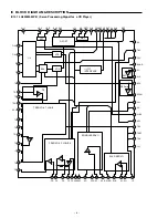
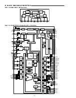
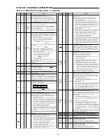
IC BLOCK DIAGRAM & DESCRIPTION
Note) The same potential must be suplied to all power supply pins, i.e., VDD,VVDD,LVDD,RVDD
and XVDD.
33
34
35
36
37
38
39
40
41
42
43
44
45
46
47
48
49
50
51
52
53
54
55
56
57
58
59
60
61
62
63
64
TEST4
PCCL
MUTEL/
CONT7
LVDD
LCHO
LVSS
RVSS
RCHO
RVDD
MUTER/
CONT8
XVDD
XOUT
XIN
XVSS
SBSY
EFLG
PW
SFSY
SBCK
FSX
WRQ
RWC
SQOUT
COIN
*CQCK
*RES
TST11
16M
4.2M
TEST5
VDD3V
TEST1
I
I
O
-
O
-
-
O
-
O
-
O
I
-
O
O
O
O
I
O
O
I
O
I
I
I
O
O
O
I
-
I
Left channel mute output pin, General-purpose 7
output pin.
Rest to MUTEL function.
Left channel power supply pin.
Left channel output pin.
Left channel ground pin. Must be connected to 0V.
Right channel ground pin. Must be connected to 0V.
Right channel output pin.
Right channel power supply pin.
Right channel mute output pin, General-purpose 8
output pin.
Rest to MUTER function.
Lch
one-bit
DAC
Rch
one-bit
DAC
Crystal oscillator power supply pin.
Connections for a 16.934MHz crystal oscillating circuit
ground pin.
Crystal oscillator ground pin. Must be connected to 0V.
Subcode block synchronization signal pin.
C1,C2,signal and double error correction monitor pin.
Subcode P,Q,R,S,T,U,V and W output pin.
Subcode frame synchronization signal output pin.
This signal falls when the subcode are in the standby stase.
Subcode readout clock input pin. This is a Schmitt input.
(Must be connected to 0V when unused.)
Output for the 7.35kHz synchronization signal divided from
the crystal oscillator pin.
Subcode Q output standby output pin.
Read/ write control input pin. This is a Schmidt input.
Subcode Q output pin.
Command, data input pin from control microprocessor.
Input for both the command input acquisition clock and the
SQOUT subcode readout clock input pin.
This is Schmidt input.
Reset input pin.
This pin must be set low briefly after power is first applied.
Test output pin. Leave open. (Notmally output a low level.)
16.9344MHz clock output pin.
4.2336MHz clock output pin.
Test input pin. A pull-down resistor is built in.
Must be connected to 0V.
Internal circuit 3.3V system power supply pin.
Test input pin.
A pull-down resistor is built in. Must be connected to 0V.
Test input pin.
A pull-down resistor is built in. Must be connected to 0V.
General-purpose I/O command identification pin.
A pull-down resistor is built in.
Used operate similarly to LC78622E connected to open or 0V.
H ; Must be connected to general-purpose port command.
L ; Be able to all command control.
No. Symbol I/O
Function description
Output pin
to rest
-
-
H output
-
-
-
-
-
-
H output
-
-
-
Incertitude
Incertitude
Incertitude
Incertitude
-
Incertitude
Incertitude
-
Incertitude
-
-
-
L output
Clock output
Clock output
-
-
-
Defect detection signal(DEF) input pin.
(Must be connected to 0V when unused.)
PLL
Test input pin. A pull-down resistor is built-in.
Must be connected to 0V.
Internal VCO ground pin.Must be connected to 0V.
External VCO control phase comparator output pin.
PDO output current adjustment resistor
connection pin.
Internal VCO power supply pin.
VCO frequency range adjustment.
Digital system ground pin. Must be connected to 0V.
Slice level
control
EFM signal output pin.
EFM signal input pin.
Test input pin. A pull down resistor is built in.
Must be connected to 0V.
Disk motor control output.
Can be set to three-value output by microprpcessor command.
Rough servo/phase control automatic switching monitor
output pin.
Outputs a high level during rough servo and a low level.
Track detection signal input pin. This is a Schmidt input.
Tracking error signal input pin. This is a Schmidt input.
Tracking off output pin.
Tracking gain switching output pin.
Increase the gain when low.
Track jump output.
Three-value output is also possible when specified by
microprocessor command.
1
2
3
4
5
6
7
8
9
10
11
12
13
14
15
16
17
18
19
20
I
I
O
-
AI
-
AI
-
O
I
I
O
O
O
I
I
O
O
O
O
-
-
-
Incertitude
-
-
L output
L output
-
-
H output
Incertitude
L output
DEFI
TAI
PDO
VVSS
ISET
VVDD
FR
VSS
EFMO
EFMIN
TEST2
CLV+
CLV-
V/*P
HFL
TES
TOFF
TGL
JP+
JP-
No. Symbol I/O
Function description
Output pin
to rest
EMF data playback clock monitor pin.
Output 4.3218MHz when the normal-speed playback phase
command.
Synchhronization signal detection output pin. Output a high
level when the synchronization signal detected from the EFM
signal and the internaly generated synchronization signal range.
Peripheral circuitry 5V system power suply pin.
General-purpose 1
input/output pin.
General-purpose 2
input/output pin.
General-purpose 3
input/output pin.
General-purpose 4
input/output pin.
General-purpose 5
input/output pin.
De-emphasis monitor pin.
A high level indicates playback of a de-emphasis disk,
General-purpose 6 output pin.
Rest to EMPH function.
C2 flag output pin.
Digital output pin. (EIJA format)
Test input pin.
A pull-down resistor is built in. Must be connected to 0V.
21
22
23
24
25
26
27
28
29
30
31
32
PCK
FSEQ
VDD
CONT1
CONT2
CONT3
CONT4
CONT5
EMPH/
CONT6
C2F
DOUT
TEST3
O
O
-
I/O
I/O
I/O
I/O
I/O
O
O
O
I
Controlled by serial data commands.
From the microprocessor.
Any of these that are unused must
be either set up as input pin and
connected to 0V, or set up as output
pin and left open.
L output
Incertitude
-
Input
L output
Incertitude
Incertitude
-
_
_
_
_
_
_
_
_
_
_
_
_
_
_
_
_
_
_
_
_
_
_
_
_
_
_
_
_
_
_
_
_
_
_
_
_
_
_
_
_
_
_
_
_
_
_
_
_
_
_
_
_
_
_
_
_
_
_
_
_
_
_
_
_
1
2
3
4
5
6
7
8
9
10
11
12
13
14
15
16
17
18
19
20
21
22
23
24
25
26
27
28
29
30
31
32
48
47
46
45
44
43
42
41
40
39
38
37
36
35
34
33
64
63
62
61
60
59
58
57
56
55
54
53
52
51
50
49
DEFI
TAI
PDO
VVSS
ISET
VVDD
FR
VSS
EFMO
EFMIN
TEST2
CLV+
CLV-
V *P
HFL
TES
EFLG
SBSY
XVSS
XIN
XOUT
XVDD
MUTER CONT8
RVDD
RCHO
RVSS
LVSS
LCHO
LVDD
MUTEL CONT7
PCCL
TEST4
TO
F
F
TGL
JP+
JP-
PCK
FSEQ
VDD
CONT1
CONT2
CONT3
CONT4
CONT5
EMPH CONT6
C2F
DOUT
TEST3
TEST1
VDD3V
TEST5
4.2M
16M
TST11
*RES
*CQOUT
COIN
SQOUT
RW
C
WRQ
FSX
SBCK
SFSY
PW
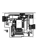
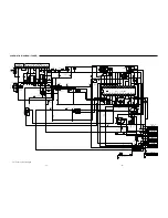
IC102 LC78629E (DSP for a CD Player)


