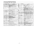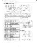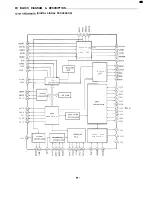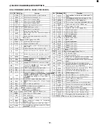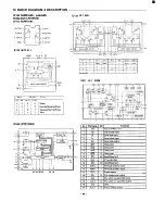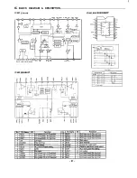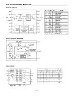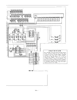
BLOCK DIAGRAM DESCRIPTION
(SERVO SIGNAL PROCESSOR)
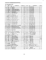
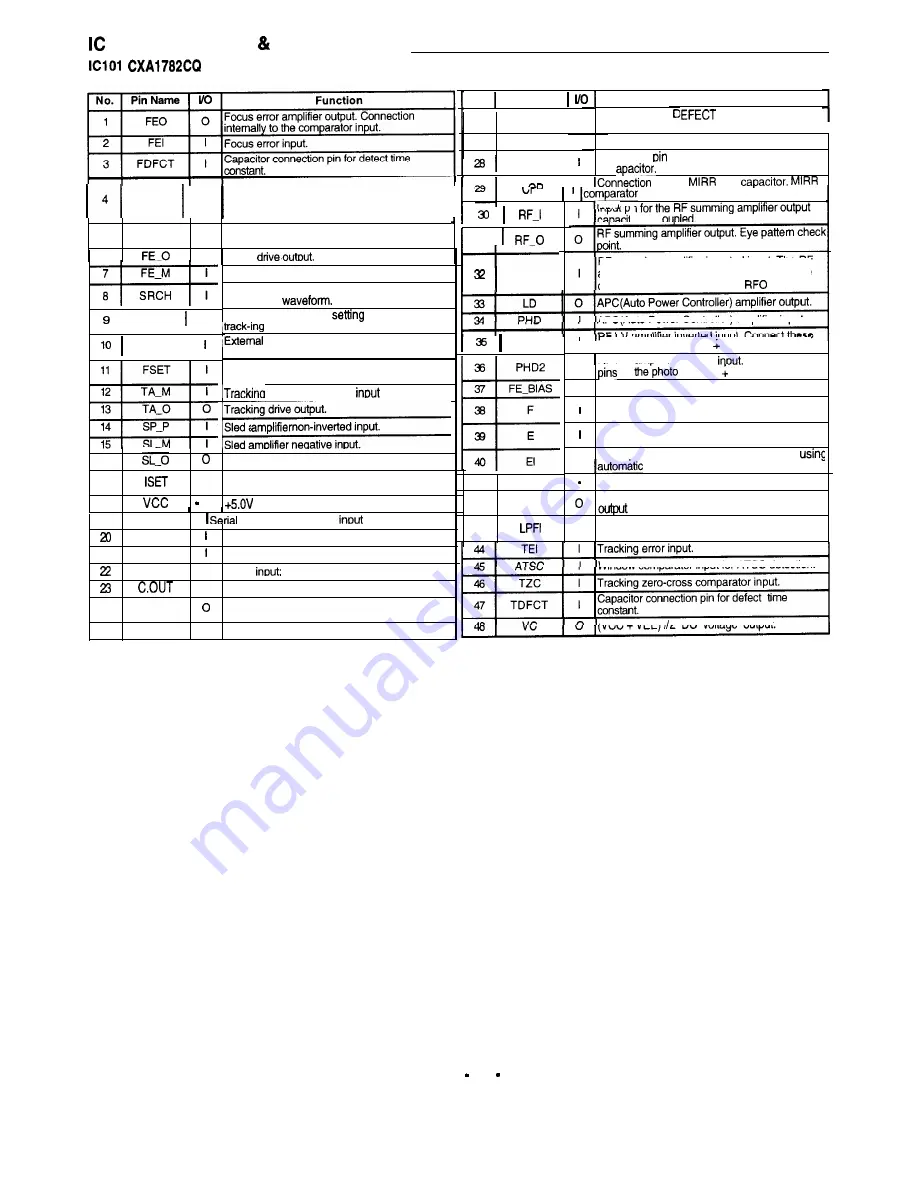
No.
PIN
NAME
Function
bottom hold output
2 6
c c 2
0
Input pin for the
c a p a c i t a n c e - c o u p l e d .
I
27
cc1 ,
I
I
DEFECT bottom hold output.
Connection
for DEFECT bottom hold
c
,
I,
pin for
h o l d
CB
non-inverted input.
-ir
ante-c
31
FGD
I
Ground this pin through a capacitor when
decreas-ing the focus servo high-frequency gain.
I
5
F L B
External time constant setting p i n f o r i n c r e a s i n g
the focus servo low frequency.
6
0 F o c u s
RF summing amplifier inverted input. The RF
a m p l i f i e r g a i n i s d e t e r m i n e d b y t h e r e s i s t a n c e
connected between this pin and
pin.
APC(Auto Power Controller) amplifier input.
RF I-V amolifier inverted input. Connect these
RF-M
Focus amplifier negative input.
External time constant setting pin for generating
focus servo
External time constant
p i n f o r s w i t c h i n g
high frequency gain.
time constant setting pin for switching
track-ing high frequency gain.
High cut off frequency setting pin for focus and
tracking phase compensation amplifier.
amolifier neaative
S l e d
non-Inverted Input.
I
TGU
I
PHD1
T G 2
I
pins to the’photo diodes A
C and B + D pins.
RF I-V amolifier inverted
Connect these
to
diodes A C and B + D pins.
I
Bias adjustment of focus error amplifier.
,
F I-V and E I-V amplifier inverted input. Connect
these pins to the photo diodes F and E.
F I-V and E I-V amplifier inverted input. Connect
these pins to the photo diodes F and E.
I-V amplifier E gain adjustment. (When not
balance adjustment.)
16
17
1 8
Sled drive output.
Setting pin for Focus search, Tracking jump and
Sled kick current.
4 1
V E E
G r o u n d
42
T E O
Tracking error amplifier output. E-F signal
43
Comparator input for balance adjustment. (Input
from TEO through LPF.)
I
I
19 I
C L K
I
I
data transfer clock
from CPU.
1
X L T
Latch input from CPU.
2 1
D A T A
Serial data input from CPU.
X R S T
I
Reset
resets at Low.
Window comparator input for ATSC detection.
(VCC + VEE) 2 DC voltage output.
.
0
Track number count signal output.
24
S E N S
Outputs FZC, DFCT, TZC, Gain, BAL, and
others according to the command from CPU.
25
F O K
0
Focus OK comparator output.
31
Summary of Contents for DC-F430AV
Page 16: ...EXPLODED VIEW CHASSIS I YOi 4 YO4 YOI d k 0 q f Y02 9 a L YO2 i y i A _ _ I ...
Page 17: ...EXPLODED VIEW CABINET U II G J I L Ei 16 ...
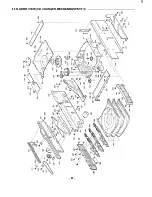
Page 29: ...EXPL ODED VIEW CD CHANGER MECHANISM PARTl 28 ...
Page 44: ... i I I ...
Page 51: ...1 I V P a CN421 C N 4 2 2 TO FRONT C N 4 2 4 TO AMP TO DECK 50 ...
Page 54: ...WIRING DIAGRAM CD ...
Page 56: ...WIRING DIAGRAM DECK 55 ...
Page 57: ... 56 ...
Page 58: ...WIRING DIAGRAM FRONT ...
Page 59: ...r e I 58 ...
Page 60: ...WIRING DIAGRAM POWER CENTER SURROUND SPEAKERS FRONT SPEAKERS SUB Ob OFE I 59 ...
Page 61: ...i I 60 ...
Page 62: ...WIRING DIAGRAM PRE AMP TUNER 61 ...
Page 63: ... 62 ...
Page 66: ...Apr 98 2300 NS Printed in Japan SANYO Electric Co Ltd Osaka Japan ...

