background image

-  4  -

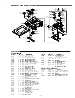
Do not remove the pick-up from base mechanism because of

adjustment difficulty.

GREASE

CDF-409

GREASE

CDF-409

GREASE

CDF-409

GREASE

EM-30LG

GREASE

EM-30LG

A

: Clean the groove by alcohol well.

A

A

GREASE

EM-30LG

GREASE

EM-30LG

Apply screw lock

GREASE

EM-30LG

GREASE

EM-30LG

4. Base mechanism mounting parts.

5. Base mechanism parts.

6. Tray parts.

MECHANISM REPLACEMENT

Summary of Contents for DVD-SL20

Page 1: ...TEP PLAY REV FWD CLEAR SEARCH MODE 1 2 3 C 4 5 6 7 8 9 0 ENT SETUP MENU AUDIO TITLE RETURN PICTURE MODE ANGLE REPLAY ZOOM ANGLE LAST MEMO SURROUND ON SCREEN PROGRAM OPEN CLOSE REPEAT A B REPEAT SUBTITLE CHANGE SUBTITLE ON OFF XE SS PA AU Schematic Diagram DVD 36 Schematic Diagram MPEG UK XE 38 Schematic Diagram MPEG AU SS PA 40 Wiring Diagram DVD MPEG A side 42 Wiring Diagram DVD MPEG A side Top L...

Page 2: ...W Max CW WAVELENGTH 790 nm VIDEO OUT AUDIO OUT R L DIGITAL OUT OPT S VIDEO OUT VIDEO OUT SELECT S RGB AV EURO CONNECTOR RGB OUT CAUTION INVISIBLE LASER RADIATION WHEN OPEN AND INTERLOCKS DEFEATED AVOID EXPOSURE TO BEAM ADVARSEL USYNLIG LASER STRÅLING VED ÅBNING NÅR SIKKERHEDSAFBRYDERE ER UDE AF FUNKTION UNDGÅ UDS ÆTTELSE FOR STRÅLING VARNING OSYNLIG LASER STRÅLNING NÄR DENNA DEL ÄR ÖPPNAD OCH SPÄR...

Page 3: ...r the initial shock the resistivity will still remain at a level of 50 to 60 G but the mechanical robustness will weaken Do not place in a dusty location The entry and deposition of dirt into or on the pickup lens or moving section will cause malfunction or degradation DVD MECHANISM REPLACEMENT Connectors Do not connect or disconnect while power is on Connecting or disconnecting signal wires or th...
Page 4: ...he 2 tray Move both the right and left 1 tray pins to the ends Remove the 2 tray Move the 1 slide to the left end Insert the 2 tray 3 2 4 1 TERMINAL ROUND HOLE ROUND HOLE SHASSIS TRIANGLE MARK BOSS SOLDERING MECHA P W B 1 Adjust the motor terminal to boss in the chassis 2 Adjust the round hole of the motor to the triangle mark of P W B and solder it ...

Page 5: ...y GREASE CDF 409 GREASE CDF 409 GREASE CDF 409 GREASE EM 30LG GREASE EM 30LG A Clean the groove by alcohol well A A GREASE EM 30LG GREASE EM 30LG Apply screw lock GREASE EM 30LG GREASE EM 30LG 4 Base mechanism mounting parts 5 Base mechanism parts 6 Tray parts MECHANISM REPLACEMENT ...

Page 6: ... Y Y Check each other connection to LOADER N Check IC800 and peripheral circuit When AC IN LOADERMO TOR turn Chec k OPEN or SHORTat pi n 64 6 8 73 and 74 of IC800 Is th e voltage at pi n3 of IC850 about 1 9V Check IC850 and peripheral circuit N Y Is th er e wa vefo rm at X8000about 3 0Vp p Check X8000 IC800 and peripheral circ uit Rewrit e ROM DATA N Y Y N Is th e volt age at pi n31 and 32 of FL60...

Page 7: ...cui t Y N A NO DI GITAL AUDI O OUT ON PLAYBACK Is there waveform at pin 4 of IC859 Is the voltage at pi n 5 of IC859 about 3 3V Y Check IC871 and peripheral circuit N N Check IC851 and peripheral circ uit Y Check IC130 and peripheral circuit Is there waveform at pin 13 1 4 15 and 16 of IC871 CheckIC800 and peripheral circui t Y N Is there waveform at pin 13 1 4 15 and 16 of IC871 Pi n 6 of IC859 i...

Page 8: ...e undefined In the following cases be sure to set up Market Region 1 When updating the system using CD R Part code 0PRADD711400A 2 When replacing a DVD substrate While Market Region information are undefined the message Region Undefined is displayed on the screen NOTE Even if the condition is not under 1 or 2 above if the message Region Undefined is displayed be sure to set up Market Region 2 Push...

Page 9: ...ket denotation push ENT button on the remote controller With each push the indicator will advance as shown below WM SFC EUR S18 SS PA 3 2 Specify the code of the model in accordance with the Market Region Setup Table above In DWM 380 model the code is the same as the initial one WM Advance to the next procedure without making any changes 3 3 Once the desired code is displayed push p button to move...

Page 10: ...tor to Exit area 5 Saving settings 5 1 Make sure that the Market and Region settings are properly set If any of the settings are incorrect you can make a change by moving the indicator using p button and following procedures 3 and 4 above 5 2 After ensuring that the settings are all correct push ENT button while the indicator is on Exit area The settings are now saved 6 Finishing settings 6 1 Afte...

Page 11: ...shing the Power button enables you to terminate the operations without making any settings HOW TO LOAD SOFTWARE FOR MPEG P W BOARD 1 Power on then open tray 2 It take on CD ROM for UPDATE software to the tray and tray close 3 Display UP DATE in the TV screen 4 For the time being tray open and FL display remain UP DATE 5 When software loading finished FL display STANDBY 6 Next set up market code an...

Page 12: ... 11 EXPLODED VIEW CABINET CHASSIS Y10 8 Y02 Y02 Y02 Y02 Y02 1 2 3 11 10 53 7 9 12 4 5 6 71 Y01 Y03 Y04 Y04 Y04 Y06 Y06 Y07 Y09 Y08 Y05 Y03 Y01 Y01 73 72 51 52 55 13 54 56 57 74 ...

Page 13: ... 323 8010 ASSY CABINET FRONT PA SS 3 614 321 2126 BUTTON OPEN CLOSE 4 614 320 3766 BUTTON PLAY 5 614 320 3889 CAP BUTTON PLAY CAP PLAY 6 614 302 0530 DEC WINDOW LED STANDBY 7 614 320 3773 BUTTON POWER 8 614 321 2331 ASSY CABINET BENDING AFTER BENDING 9 614 320 3728 ASSY CABINET BOTTOM 10 614 313 6545 SPRING PLATE SHIELD 11 614 129 1901 FIXER AC CORD or 614 284 1884 FIXER AC CORD 12 614 321 8951 PA...

Page 14: ... 2409 MT POLYEST 0 1U M 250V C4908 404 080 8107 CERAMIC 2200P M 400V CN481 614 310 2557 PLUG 14P or 645 006 0892 PLUG 14P D4802 408 043 6704 DIODE RGP10GL 22C 012 D4803 408 044 7304 DIODE SB160L 19C2 004 D4805 408 043 6704 DIODE RGP10GL 22C 012 D4806 408 043 6704 DIODE RGP10GL 22C 012 D4807 407 099 4603 ZENER DIODE MTZJ3 9B D4809 408 044 6307 DIODE SB140L 19C2 004 D4820 407 099 6607 ZENER DIODE MT...

Page 15: ...C851 409 509 9208 IC PQ070XZ01Z IC852 409 509 9208 IC PQ070XZ01Z IC859 409 489 9700 IC NC7SZ157P6 IC871 409 500 3304 IC PCM1748E DAC_2CH IC872 409 426 1903 IC KIA4558F or 409 039 7804 IC NJM4558M L1001 645 034 7887 INDUCTOR 1000 OHM or 645 020 1813 INDUCTOR 1000 OHM L1090 645 034 7887 INDUCTOR 1000 OHM or 645 020 1813 INDUCTOR 1000 OHM L1100 645 034 7887 INDUCTOR 1000 OHM or 645 020 1813 INDUCTOR ...

Page 16: ...812 M6 Q8881 405 146 1704 TR KTA1504 Y or 405 146 9700 TR KTA1504 GR or 405 134 5905 TR 2SA1037AK R or 405 002 0308 TR 2SA1037K R or 405 005 5508 TR 2SA812 M6 Q8882 405 159 0503 TR KRC107S or 405 141 5608 TR DTC114YKA S8400 645 040 6102 SWITCH SLIDE 2P 2TX4 SG841 645 045 7449 SURGE ABSORBER SG842 645 045 7449 SURGE ABSORBER SG871 645 045 7449 SURGE ABSORBER SG872 645 045 7449 SURGE ABSORBER X1300 ...

Page 17: ...Z 2 6X10X0 5 BASE FIX DM19 614 321 0634 ASSY MECHA KIT 700 BASE BASE MECHA DM20 411 184 0302 SCR S TPG PAN PCS 1 7X4 5 RACK FIX DM21 614 310 2083 GEAR RACK MOVE PICKUP FREE DM22 614 310 6159 SPRING COMP FOR BACK RUSH RACK DM23 614 310 2076 GEAR RACK MOVE PICKUP FIX DM24 411 018 4704 SCR PAN PCS 1 7X5 LIMIT SW FIX DM25 645 040 9899 SWITCH MICRO 1P 2T LIMIT SW DM26 412 057 8304 SPECIAL WASHER FOR GE...

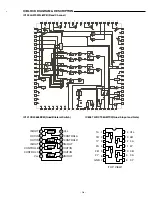
Page 18: ...10 S11 S12 S13 S14 S15 S16 5G S1 S2 S3 S4 S5 S6 S7 S8 S9 S10 S11 S12 S13 S14 S15 6G S1 S2 S3 S4 S5 S6 S7 S8 S9 S10 S11 S12 S13 S14 S15 S16 7G S1 S2 S3 S4 S5 S6 S7 S8 S9 S10 S11 S12 S13 S14 S15 8G S1 S2 S3 S4 S5 S6 S7 S8 S9 S10 S11 S12 S13 S14 S15 1 2 3 4 5 6 7 8 9 10 11 12 13 14 15 16 F1 F1 NP P1 P2 P3 P4 P5 P6 P7 P8 P9 P10 P11 P12 P13 PIN No CONNECTION 17 18 19 20 21 22 23 24 25 26 27 28 29 30 31...

Page 19: ...ral Switch 1 2 3 4 5 6 7 8 9 10 11 12 13 14 SW C SW D SW B SW A VDD CONTROL A CONTROL D IN OUT OUT IN OUT IN IN OUT IN OUT OUT IN OUT IN IN OUT CONTROL B CONTROL C VSS IC806 74VHCT08AMTCX Quad 2 Input and Gate TOP VIEW 14 13 12 11 10 9 8 1 2 3 4 5 6 7 1A 1B 1Y 2A 2B 2Y GND Vcc 4B 4Y 4A 3B 3A 3Y ...

Page 20: ... terminal Focus offset adjustment terminal Tracking offset adjustment terminal Bottom hold detect constant setting register connection terminal BCA output Pin No Pin name Function 46 DEF Defect output H Defect detection 47 DEFC Defect detection condenser connect terminal 48 TC Defect detection constant setting register terminal 49 GND GND DTD system 50 LPC RF DC servo condenser connect terminal 51...

Page 21: ...Address Stlobe Lower Byte Control Write Enable Output Enable Data Input Output Power 5V Ground No Connec A0 A8 RAS CASH CASL WE OE VCC VSS NC I O1 I O16 Input Input Input Input Input Input Supply Ground Input Output 16 19 22 26 14 28 29 13 27 1 6 20 21 35 40 11 12 15 30 2 5 6 10 31 34 36 39 WE RAS CASL CASH OE I O1 I O2 I O3 I O4 I O5 I O6 I O7 I O8 VSS VSS I O16 I O15 I O14 I O13 I O12 I O11 I O1...

Page 22: ...N 1 SI 2 7 EEPROM 8 VCC 4 GND 7 WP 3 A2 2 A1 1 A0 6 SCL 5 SDA DEVICE ADDRESS COMPARATOR START STOP LOGIC SERIAL CONTROL LOGIC H V PUMP TIMING DATA RECOVERV EEOROM SERIAL MUX DOUT ACK LOGIC V DEC DATA WORD ADDR COUNTER R W DIN DOUT LOAD INC COMP LOAD FN X DEC IC490 STR G6351LF1129 Switching Regulators DCP Comp UVI O 4 REG OSC 1 2 5 3 VIN D S OCP FB Tri GND Terminal No Symbols Description Functions ...

Page 23: ...MA controller 8ch Bus converter 32bits 16bits Port0 to portB RAM 2Kbytes 1 2 3 4 5 6 7 8 9 10 11 12 13 14 15 16 17 18 19 20 21 22 23 24 25 P21 D17 P22 D18 P23 D19 P24 D20 P25 D21 P26 D22 P27 D23 P30 D24 P31 D25 P32 D26 P33 D27 P34 D28 P35 D29 P36 DD30 VSS P37 D31 P40 A00 VCC P41 A01 P42 A02 P43 A03 P44 A04 P45 A05 P46 A06 P47 A07 PD3 AN3 INT5 PD2 AN2 DVDSOS PD1 AN1 STREQ DRVVLD PD0 AN0 STRBIN AVSS...

Page 24: ...ionally SC2 UART1 clock I O Clock output can be used when UART1 clock output is enabled PE3 General purpose I O port This function is valid when UART1 clock output is disabled DREQ0 1 Input of DMA external transfer request This input is used from time to time when this pin is selected for the DMAC transfer cause Therefore it is needed to stop output by other functions except when such output is pe...

Page 25: ... purpose I O port This function is valid when STREQ output is disabled DRVVLD DRVVLD input This input isused from time to time while input operation is selected Therefore it is needed to stop output by other functions except when such output is performed intentionally AN2 A D converter analog input This input is used from time to time while input operation is selected Therefore it is needed to sto...

Page 26: ...n outputs the same clock frequency as the external bus operating frequency PA6 When the pin is not used for this purpose it can be used as a general purpose I O port RAS output of DRAM bank 0 CASL output of DRAM bank 0 CASH output of DRAM bank 0 WE output of DRAM bank 0 RAS output of DRAM bank 1 CASL output of DRAM bank 1 CASH output of DRAM bank 1 WE output of DRAM bank 1 See the description of t...

Page 27: ... X16MIN X16MOUT DVDCKIN DVDCKOUT VPDO VCOC VRFFR HDAT 7 0 HADR 12 0 HRDB HWRB HCSB HWAITB HBUSYB HFBUSYB HIRQOB PP 7 0 FDO TDO SLDO SPDO SGC TBAL FBAL OFFSET BACTH BOOT3T RFVCA HFLBIAS TESBIAS SLCBIAS TEST0 HFLIO WRQ EMPH PW SBCK SBSY SFSY FSX EFLG DOUT LRSY ROMCK ROMXA C2F MD 15 0 MA 12 0 MRASOB MRASIB MCASUB MCASLB MOEB MWEB AVACKOI AVREQIO AVDENB AVSCTB AVERRB AVD 7 0 A D Block D A Block Servo ...

Page 28: ...pin EVENT counter input pin Mirror detest signal I O pins General purpose port 0 General purpose port 1 General purpose port 2 General purpose port 3 Subcode Q ready monitor pin DSP command dispose busy signal output pin DSP command reseiver busy signal output pin I O power Digital 3 3V or 5V 42 to 97 Digital GND Supplementation Wait signal output pin Interrupt signal output pin Decoder reset inpu...

Page 29: ...L JV power supply Analog 5V Analog GND JV control pin JV control pin Supplementation EFM playback PLL clock jitter output pin JV control pin JV control pin SYSTEM PLL power supply Analog 3 3V Analog GND DRAM data 15 DRAM data 14 DRAM data 13 DRAM data 12 DRAM data 11 DRAM data 10 DRAM data 9 DRAM data 8 I O power supply Digital 3 3V or 5V 159 or 197 Digital GND DRAM data 7 DRAM data 6 DRAM data 5 ...

Page 30: ...put Pin N Channel Open Drain This pin outputs scrial data at the falling cdge of the shift clock starting from the lower bit Data Input Pin This pin inputs serial data at the rising cdge of the shift clock starting from the lower bit Clock Input Pin This pin reads serial data at the rising cdge and outputs data at the falling cdge Serial Interface Strobe Pin The data input after the STB has fallen...

Page 31: ...8 A15 A18 A10 DQ15 DQ0 CE OE WE BYTE RY BY WP RESET VDD VSS Pin Name Bank Selective Address Flush Bank Address Flush Bank Block Address Flush Bank Sector Sddress Data Input Output Chip Enable Output Enable Write Enable Bait Pin Ladey Beje Output Write Protect Reset Power Supply Ground Functions Selects bank 1 when L and bank 2 Sapply address for flush bank Select flush bank for erease Select flush...

Page 32: ...ve Mskes data output Hi Z ISHZ sfter the clock and masks the output Blocks data input when L U DQM active Data inputs outputs are multiplexed on the same pins Power and ground for the input buffers and the core logic Isolated power supply and ground for the output buffers to provide improved noise immunity This pin is recommended to be left No Connection on the device Pin CLK CS CKE A0 A10 AP BA R...

Page 33: ...t for R channel Analog ground Common voltage decoupting Zero flag output for R channel Zero flag output for L R channel Zero flag output for L channel No assign Mode control data input Mode control clock input Mode control latch input System clock input PIN ASSIGNMENTS Output Amp and Low pass Filter Oversampling Digital Filter with Function Controller Audio Serial Port Serial Countrol Port System ...

Page 34: ... SWITCH SPINDLE MOTOR LOADING MOTOR OPEN CLOSE SWITCH CN811 14P CN481 14P CN870 AUDIO VIDEO OUT S VIDEO OUT DIGITAL OUT CN872 CN871 CN895 12P DVD MPEG P W B FRONT P W B DVD MECHANISM AC IN CN491 CN490 FU490 1A L 125V DENGEN P W B WH 11P A V EURO CONNECTOR RGB OUT SCART P W B CN891 11P UK XE Only This is a basic wiring connection ...

Page 35: ... 1AD2SHF0179 TO SOCKET E CN661 J6641 D6602 C6611 C6612 D6604 D6601 D6603 R6603 D6605 L6601 C6606 J6616 J6614 J6613 J6611 J6609 C6610 C6609 J6608 J6604 J6606 J6603 J6612 J6607 D6611 L6606 J6671 CN660 Q6601 R6605 R6604 J6615 J6610 J6605 J6602 J6617 J6618 C6625 C6626 D6610 D6609 D6608 D6607 C6622 C6619 C6616 C6613 R6606 SH CAN GND OPEN CLOSE MLD1 MLD2 CLOSE_SW GND OPEN_SW S003 94HB 1AD4B10D1000A S000...

Page 36: ...SANYO Electric Co Ltd OSAKA JAPAN Mar 02 BB Printed in Japan ...

Reviews: