background image


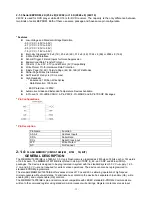
2-1-5 512K X 16 Bit X 2 Banks Synchronous DRAM (A43L0616) 


Features 

„

  JEDEC standard 3.3V power supply 

„

  LVTTL compatible with multiplexed address 

„

  Dual banks / Pulse RAS 

„

  MRS cycle with address key programs 

-


CAS Latency (2,3) 

-


Burst Length (1,2,4,8 & full page) 

-


Burst Type (Sequential & interleave) 

„

  All inputs are sampled at the positive going edge of the system clock 

„

  Burst Read Single-bit Write operation 

„

  DQM for masking 

„

  Auto & self refresh 

„

  64ms refresh period (4K cycle) 

„

  50 Pin TSOP (II) 


- 25 - 

Summary of Contents for DVD1451U

Page 1: ...GB SERVICE MANUAL DVD1451U MPEG4 PLAYER SERVICE MANUAL ...

Page 2: ...2 1 2 DVD Processor Chip MTK1389F 7 2 1 3 Serial EEPROM 2K 256 x 8 24C02 or 16 K 2048 x 8 24C16 22 2 1 4 FLASH MEMORY CMOS 16M 2M 8 1M 16 BIT 22 2 1 5 512K X 16 Bit X 2 Banks Synchronous DRAM A43L0616 25 3 PRODUCT SPECIFICATIONS 28 4 UPGRADING SYSTEM AND CHANGING THE REGION CODE 29 5 OPERATING INSTRUCTION 30 MAINTENANCE TROUBLESHOOTING 30 6 DISASSEMBLY AND REASSEMBLY 32 7 TROUBLESHOOTING 33 8 BLOC...

Page 3: ...or a metering system that complies with American National Standards institute ANSI C101 1 Leakage Current for Appliances and underwriters Laboratories UL 1270 40 7 With the instrument s AC switch first in the ON position and then in the OFF position measure from a known earth ground metal water pipe conduit etc to all exposed metal parts of the instrument antennas handle brackets metal cabinets sc...

Page 4: ...Before servicing Instruments covered by this service manual and its supplements read and follow the Safety Precautions section of this manual Note If unforeseen circument create conflict between the following servicing precautions and any of the safety precautions always follow the safety precautions Remember Safety First 1 2 1 General Serving Precautions 1 a Always unplug the instrument s AC powe...

Page 5: ...st 2 after removing an electrical assembly equipped with ESD devices place the assembly on a conductive surface such as aluminum foil to prevent electrostatic charge buildup or exposure of the assembly 3 Use only a grounded tip soldering iron to solder or unsolder ESD device 4 Use only an anti static solder removal devices Some solder removal devices not classified as anti static can generate elec...

Page 6: ... Descriptions 2 1 1 DVD SANYO HD65 PUH Connector Pin Definition I F Signals I O Pin F 1 F 2 T 3 T 4 C 5 D 6 CD DVD 7 RF 8 A 9 B 10 F 11 GND PD 12 VC 13 VCC 14 E 15 NC 16 VR CD 17 VR DVD 18 LD CD 19 MD 20 HFM 21 NC 22 LD DVD 23 GND LD 24 5 ...

Page 7: ...or Error Correction PLI Focus Tracking Loading AuDdio AMP Video D A Filter 1 F Conn front pannel Spindle Motor Focus Coil Track Coil Sied Motor Loading Motor BA5954FP 4ch motor Drive 24CO2 System Controller Fiash Memory 8Mbit Disc SDROM Disc motor unit Laser pickup 6 ...

Page 8: ...s regional code encrypted RCE DVDs z Selectable 4 3 Pan Scan or 16 9 Widescreen format z PAL NTSC playback z Multi speed FF RW slow motion multi level zoom High Performance Analog RF Amplifier z Programmable fc z Dual automatic laser power control z Defect and blank detection z RF level signal generato Audio z Dolby Digital AC 3 EX decoding z DTS DTS ES decoding z MLP decoding for DVD Audio z MPEG...

Page 9: ... Pinout Diagram 8 ...

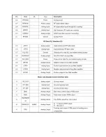
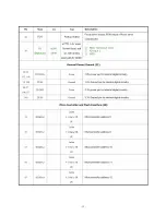
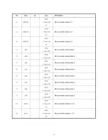
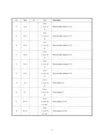
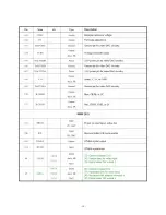
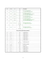
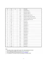
Page 10: ...PIN DESCRIPTON 9 ...

Page 11: ... 10 ...

Page 12: ... 11 ...

Page 13: ... 12 ...

Page 14: ... 13 ...

Page 15: ... 14 ...

Page 16: ... 15 ...

Page 17: ... 16 ...

Page 18: ... 17 ...

Page 19: ... 18 ...

Page 20: ... 19 ...

Page 21: ... 20 ...

Page 22: ... 21 ...

Page 23: ...able z 8 Pin and 14 Pin JEDEC SOIC 8 Pin PDIP 8 Pin MSOP and 8 Pin TSSOP Packages Pin Configurations Pin Description Pin Name Function A0 A2 Address Inputs SDA Serial Data SCL Serial Clock input WP Write Protect NC No Connect 2 1 4 FLASH MEMORY CMOS 16M 2M 8 1M 16 BIT GENERAL DESCRIPTION The MBM29LV160TE BE is a 16M bit 3 0 V only Flash memory organized as 2M bytes of 8 bits each or 1M words of 16...

Page 24: ... Internally generated and regulated voltages are provided for the program and erase operations A low VCC detector automatically inhibits write operations on the loss of power The end of program or erase is detected by Data Polling of DQ7 by the Toggle Bit feature on DQ6 or the RY BY output pin Once the end of a program or erase cycle has been completed the device internally resets to the read mode...

Page 25: ... 24 ...

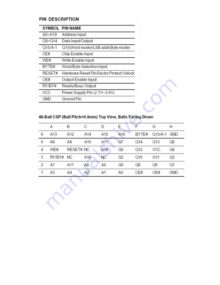
Page 26: ...address Dual banks Pulse RAS MRS cycle with address key programs CAS Latency 2 3 Burst Length 1 2 4 8 full page Burst Type Sequential interleave All inputs are sampled at the positive going edge of the system clock Burst Read Single bit Write operation DQM for masking Auto self refresh 64ms refresh period 4K cycle 50 Pin TSOP II 25 ...

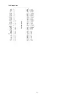
Page 27: ...Pin Configuration 26 ...

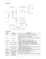
Page 28: ...ivated during row address latch time Selects band for read write during column address latch time RAS Row address Strobe Latches row addresses on the positive going edge of the CLK with RAS low Enables row access precharge CAS Column Address Strobe Latches column addresses on the positive going edge of the CLK with CAS low Enables column access WE Write Enable Enables write operation and Row prech...

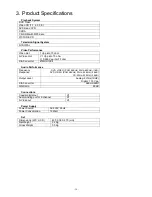
Page 29: ...rter 27MHz 10bit Audio Performance Frequency Response DVD VIDEO PCM 96KHz 20Hz 44KHz 1dB DVD VIDEO PCM 48KHz 20Hz 22KHz 0 5dB CD 20Hz 22KHz 0 5dB Output Level Analog 2Vrms 1KHZ Digital 1 15 Vpp D A Converter 96KHz 24bit S N Ratio 90dB Connections Coaxial digital out X1 Audio Analog out for 2 channel X1 S Video out X1 Power Supply Power Source AC 230V 50Hz Power Consumption 15 Watt Set Dimensions W...

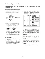
Page 30: ...4 Do not shut down the player during upgrade it will restart automatically after upgrade 5 Upgrade finish How to change the region code 1 Power on the machine and press OPEN button to push the tray out 2 Press SETUP button to enter the SETUP menu and go to the PREFERENCE item by pressing left button then press 5 buttons in turn 4 9 5 4 0 3 A edit box will be displayed you can change the region cod...

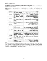
Page 31: ...istorted TV system Connect this player to a PAL NTSC compatible TV DISC TYPE Content Size Total Play time About 2hrs Single side single layer About 4hrs Single side double layer About 4hrs Double side Single layer DVD AUDIO VIDEO 12CM About 8hrs Double side double layer CD DA AUDIO 12CM About 74 minutes MP3 AUDIO 12CM About 300 minutes To handle clean and protect discs Do not touch the playing sid...

Page 32: ... compatible disc Check the disc format and its colour system T do he disc is placed upside wn Load a compatible disc Check the disc format and its colour system The disc not put in the tray correctly Check disc is put in correctly Disc is dirty Clean the disc Player setting are incorrect Change the setting via the setup menu The player does not work Parental lock is in effect Disable this function...

Page 33: ... 32 6 Disassembly and Reassembly ...

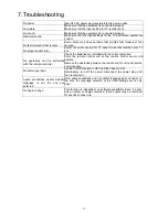
Page 34: ...rformed with the remote controller Point the remote control unit at the remote control sensor and operate Check the batteries are installed with the correct polarities Remove the obstacles between the remote control unit and remote control sensor No button operation Set the POWER button to OFF and then back to ON Alternatively turn off the power disconnect the power plug and then reconnect it Audi...

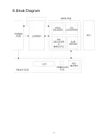
Page 35: ... 34 8 Block Diagram ...

Page 36: ...VDD18 133 RA1 134 RA2 135 RA3 136 RCLK 137 DVDD3 138 CKE 139 RA11 140 RA9 141 RA8 142 RA7 143 RA6 144 RA5 145 RA4 146 DVDD18 147 GPIO3 148 GPIO4 149 DVSS 150 GPIO5 151 ABCK 152 ACLK 153 ALRCK 154 ASDATA0 155 ASDATA1 156 ASDATA2 157 ASDATA3 158 MC_DATA 159 SPDIF 160 DACVDDC 161 VREF 162 FS 163 DACVSSC 164 CVBS 165 DACVDDB 166 DACVSSB 167 DACVDDA 168 G Y SY CVBS 169 DACVSSA 170 B CB SC 171 R CR CVBS...

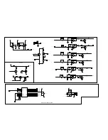
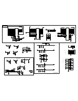
Page 37: ... 3 REGO2 4 VINSL 5 REGO1 6 FWD 7 REV 8 VCC 9 VOTR 10 VOTR 11 VOSL 12 VOSL 13 VOFC 14 VOFC 15 VOTK 16 VOTK 17 VOLD 18 VOLD 19 VCC2 20 NC 21 VCTL 22 GND 23 VINLD 24 NC 25 TRB2 26 VINTK 27 BIAS 28 MUTE U6 R50 10K C75 0 1U Q22 SS8550 Q23 SS8550 D10 D11 R52 75 R58 10K R59 10K R62 10K R64 10K C23 0 1U E1 100U 16V C2 0 1U R7 0 OR NC R8 10K R14 0 OR NC R15 0 OR NC R16 0 OR NC R17 0 OR NC FB26 FB25 FB31 FB...

Page 38: ...6 J8 YUV R72 75 C54 220P C58 100P L5 L D2 1N4148 D3 1N4148 D9 1N4148 D8 1N4148 L8 L C61 100P C57 220P R75 75 D7 1N4148 D6 1N4148 L7 L C60 100P C56 220P R74 75 L6 L C59 100P C55 220P R73 75 1 VCC1 2 DQ0 3 DQ1 4 GND1 5 DQ2 6 DQ3 7 VCC2 8 DQ4 9 DQ5 10 GND2 11 DQ6 12 DQ7 13 VCC3 14 LDQM 15 WE 16 CAS 17 RAS 18 CS 19 BS A11 20 A10 21 A0 22 A1 23 A2 24 A3 25 VCC4 26 GND3 27 A4 28 A5 29 A6 30 A7 31 A8 32 ...

Page 39: ......
Page 40: ... 1w R7 1k R9 560 R12 10K R10 680 0 5W R15 1K 1 C6 104 NC Z5 12V 0 5W L2 BLN0X Z3 3 3V 0 5W C5 103 1 2 3 4 5 6 7 8 9 MPOW 9Pin2 5mm 1 2 3 4 5 FPOW 5Pin2 5mm 1 2 3 4 MIC 4Pin2 5mm 3 3V GND 5V 5V GND 12V 12VV GND MIC 12V 12V MIC GND 5V VFD VFD 23V GND R17 0 C20 open 1 2 4 12 5 7 6 11 9 10 8 T01 TRANS2 4 C9 103 C14 220uF 16V L7 5uH 3A NC D14 NC HER303BL D16 IN5401 D15 IN5401 C26 0 1U 275VAC C24 102 X1...

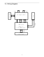
Page 41: ... Wiring Diagram Transformer Tuner AV Output Board MPEG Board Front Panel Power Power Output to Amplifier Output to TV Audio stream Video stream Control Stream Control Stream Loader is on the MPEG board 38 ...

Reviews: