No. 5995-9/34
LC78626KE
Continued from preceding page.
Pin
Pin
I/O
Description
Output pin states
No.
Name
during reset
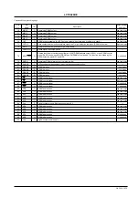
34
CONT3/SBCK
I/O
Input mode
35
CONT4/SFSY
I/O
Input mode
36
CONT5/PW
I/O
Input mode
37
SBSY
O
Subcode block sync signal output
Undefined
38
TEST3
I
Test input. Equipped with an internal pull-down resistor. Must be connected to 0 V.
—
39
DOUT
O
Digital output. EIAJ format.
Undefined
40
TEST4
I
Test input. Equipped with an internal pull-down resistor. Must be connected to 0 V.
—
41
16M/NGJ
O
Clock output
42
4.2M
O
4.2336 MHz output
Clock output
43
EFLG
O
C1, C2, one error, two error error correction monitor output
Undefined
44
FSX
O
7.35 kHz sync signal output (frequency divided from the crystal oscillator).
Undefined
45
EMPH
O
Deemphasis monitor output. When high level, a deemphasis disk is being played back.
Low-level output
46
C2F
O
C2 flag output
Undefined
47
TOUT
O
Test output. Under normal operation, this should be left open.
Undefined
48
MR1
I
DRAM switch: high : 1M, low : 4M
—
49
MR2
I
1 M: high, low 4 M: low, low 16 M: low, high 4 M X 2: high, high (MR1, MR2)
50
TESD
I
Test input. Must be connected to 0V.
—
51
MUTESL
O
L channel mute output
High-level output
52
LV
DD
P
L channel power supply
—
53
LCHO
AO
L channel output
—
54
L/RV
SS
P
For the one-bit D/A
L/R channel ground. Must be connected to 0 V.
—
55
RCHO
AO
converter
R channel output
—
56
RV
DD
P
R channel power supply
—
57
MUTER
O
R channel mute output
High-level output
58
XV
DD
P
Crystal oscillator power supply
—
59
XOUT
O
16.9344 MHz crystal oscillator connection
—
60
XIN
I
61
XV
SS
P
Crystal oscillator ground. Must be connected to 0 V.
—
62
RWC
I
Read/write control input. Schmidt input.
—
63
COIN
I
Microcontroller command input
—
64
CQCK
I
Input pin for the command input latch clock and the subcode readout clock. Schmitt input.
—
65
SQOUT
O
Subcode Q output
Undefined
66
WRQ
O
Subcode Q output standby output
Undefined
67
FMT
I
Operating mode switch: high: shock proof, low: through.
—
68
EMPP
O
DRAM empty (an RZP pulse is output when the DRAM is empty).
Low-level output
69
RES
I
External reset input: low reset (all internal blocks are reinitialized).
—
Continued on next page.
General I/O pin 3. This controls the commands from the microcontroller. This pin is shared exclusively with
the subcode read clock input (SBCK). When not used, either set this as an input port and connect to 0 V, or
set this as an output port and leave it open.
General I/O pin 4. This controls the commands from the microcontroller. This pin is shared exclusively with
the subcode frame sync signal output (SFSY). When not used, either set this as an input port and connect
to 0 V, or set this as an output port and leave it open.
General I/O pin 5. This controls the commands from the microcontroller. This pin is shared, exclusively, with
the subcode P, Q, R, S, T, U, V, W output (PW). When not used, either set this as an input port and connect
to 0 V, or set this as an output port and leave it open.
Shared function pin that functions either as the 16.9344 MHz output (16M) or as the C2 flag data continuity check
start signal (detection start is indicated by a low to high transition). Controlled by microcontroller commands.


