12
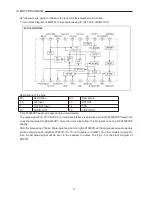
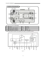
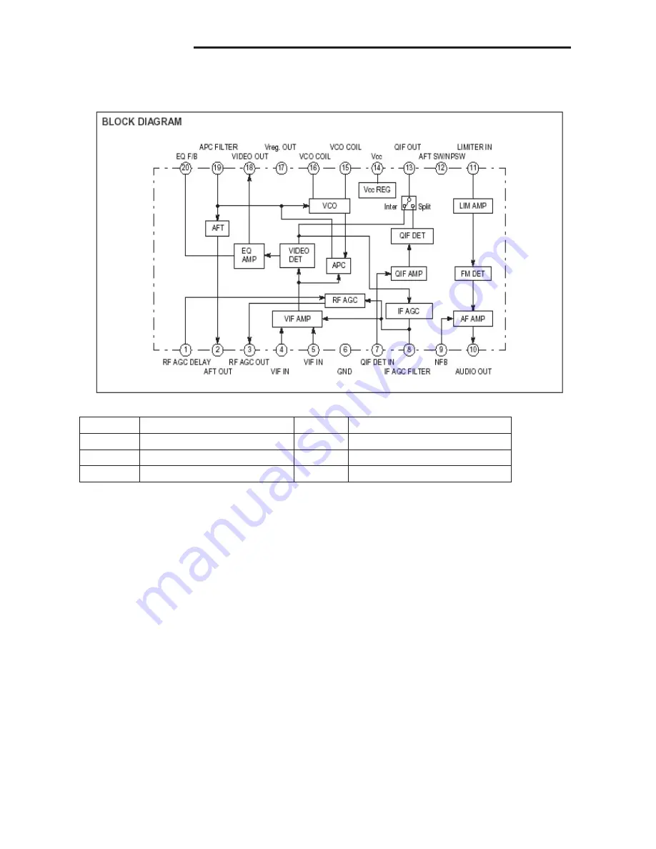
As follows we are going to introduce the inner IC block diagram and function.
1. Inner block diagram of M52760 IF signal processing IC (AFT, QIF, VIDEO OUT)
Descriptions of the pins:
Pin Description
Pin Description
4, 5
VIF input
13
QIF OUT
7 1ST_SIF
input
14
VCC
10
AUDIO OUT
18
VIDEO OUT
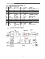
2. R2S15900SP audio processor with surround stereo
The audio signal from YPrPb/YcrCb or VGA input interface is selective sent to R2S15900SP through the
multi-channel selector HEF4052BT, while the audio signal from the AV inputs is sent to R2S15900SP
directly.
After the processing of bass, treble, balance and AVL by R2S15900S, all these processed audio signals
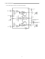
will be output to audio amplifier TPA1517 (for 15 inch models) or AN5277 (for other models) to amplify,
then the amplified signal will be sent to the speaker to output. The Fig.1-3 is the block diagram of
AN5277.
12
IC BLOCK DIAGRAM
LCD-20XR1AU.indd Sec1:12
LCD-20XR1AU.indd Sec1:12
2006/07/13 11:59:26
2006/07/13 11:59:26
Summary of Contents for LCD-20XR1/AU
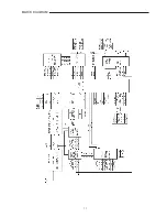
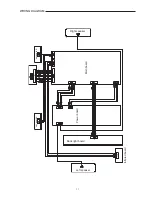
Page 13: ...11 BLOCK DIAGRAM ...
Page 16: ...14 4 Inner block diagram of TPA1517 6W stereo audio amplifier 14 IC BLOCK DIAGRAM ...
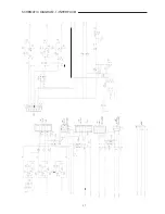
Page 23: ...21 SCHEMATIC DIAGRAM 1 INTERFACE ...
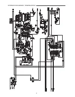
Page 24: ...22 SCHEMATIC DIAGRAM 2 TUNER AUDIO ...
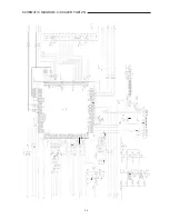
Page 25: ...23 TO INFRARED BORAD SCHEMATIC DIAGRAM 3 SCALER FLI8125 ...
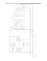
Page 26: ...24 SCHEMATIC DIAGRAM 4 FLASH ...
Page 27: ...25 SCHEMATIC DIAGRAM 5 OUTPUT POWER KEY BOARD ...
Page 28: ...26 SCHEMATIC DIAGRAM 6 POWER BOARD INFRARED BOARD ...
Page 29: ...27 EXPLODED VIEW 1 2 3 4 5 6 7 8 9 10 11 12 13 14 15 16 17 18 19 20 21 22 23 ...


