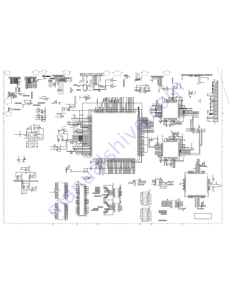
background image

A12

SCH_KJ6A

D1FM3G

D1833

1

2 3 4

5

6

X

K47B

1

1

2

2

3

4

5

6

7

8

9

10

11

12

13

14

15

16

17

18

19

20

21

22

23

24

25

26

27

28

29

30

31

32

33

34

35

36

37

38

39

40

41

42

43

44

45

46

47

48

49

49

50

50

51

52

53

54

55

56

57

58

59

60

61

62

63

64

65

66

67

68

69

70

71

72

73

74

75

76

77

78

79

80

81

82

83

84

85

86

87

88

89

90

91

92

93

94

95

96

97

98

99

99

100

100

101

102

103

104

105

106

107

108

109

110

111

112

113

114

115

116

117

118

119

119

120

120

D1FM3G

D1832

D1FM3G

D1831

J10QG305G

K8E

1

1

2

2

3

4

5

6

7

8

9

10

11

12

13

14

15

16

17

18

19

20

21

22

23

24

25

26

27

28

29

29

30

30

1

2

1A

3

1B

4

5

6

7

8

GND

9

10

11

12

13

2B

14

2A

15

16

VCC

1

2

3

4

5

6

7

8

9

10

11

12

13

14

15

16

1

2

3

4

5

1

CTL1

2

FLG1

3

FLG2

4

CTL2

5

OUT2

6

GND

7

IN

8

OUT1

1

VCCA

2

DIR

3

A1

4

A2

5

A3

6

A4

7

A5

8

A6

9

A7

10

A8

11

GND

12

GND

13

GND

14

B8

15

B7

16

B6

17

B5

18

B4

19

B3

20

B2

21

B1

22

23

NC

24

VCCB

1

VCCA

2

DIR

3

A1

4

A2

5

A3

6

A4

7

A5

8

A6

9

A7

10

A8

11

GND

12

GND

13

GND

14

B8

15

B7

16

B6

17

B5

18

B4

19

B3

20

B2

21

B1

22

23

NC

24

VCCB

1SS355

D1834

1SS355

D1837

1SS355

D1836

AH

Q1861

1

2

3

4

5

1

NC

2

NC

3

NC

4

NC

5

Vout

6

NC

7

GND

8

VCC

9

NC

10

NC

11

NC

12

NC

13

NC

14

NC

15

NC

16

NC

J10QF035G

K8A

1

2

3

1

2

3

4

5

1

2

3

4

5

1

2

3

4

5

6

7

8

9

10

11

12

13

14

15

16

17

18

19

20

1

2

3

4

5

1

2

3

4

5

6

7

8

9

10

11

12

13

14

15

16

17

18

19

20

21

22

23

24

25

26

27

28

29

30

31

32

33

34

35

36

37

38

39

40

41

42

43

44

45

46

47

48

49

50

51

52

53

54

55

56

57

58

59

60

61

62

63

64

65

66

67

68

69

70

71

72

73

74

75

76

77

78

79

80

81

82

83

84

85

86

87

88

89

90

91

92

93

94

95

96

97

98

99

100

101

102

103

104

105

106

107

108

109

110

111

112

113

114

115

116

117

118

119

120

121

122

123

124

125

126

127

128

129

130

131

132

133

134

135

136

137

138

139

140

141

142

143

144

145

146

147

148

149

150

151

152

153

154

155

156

157

158

159

160

161

162

163

164

165

166

167

168

169

170

171

172

173

174

175

176

177

178

179

180

181

182

183

184

185

186

187

188

189

190

191

192

193

194

195

196

197

198

199

200

201

202

203

204

205

206

207

208

209

210

211

212

213

214

215

216

217

218

219

220

221

222

223

224

225

226

227

228

229

230

231

232

233

234

235

236

237

238

239

240

1

OU

T

2

VD

D

3

VS

S

41

DQ13

42

DQ6

43

DQ14

44

DQ7

45

DQ15/A-1

46

VSS

47

48

A16

1

A15

2

A14

3

A13

4

A12

5

A11

6

A10

7

A9

8

A8

9

A19

10

N.C.

11

12

13

N.C.

14

N.C.

15

16

A18

17

A17

18

A7

19

A6

20

A5

21

A4

22

A3

23

A2

24

A1

25

A0

26

27

VSS

28

29

DQ0

30

DQ8

31

DQ1

32

DQ9

33

DQ2

34

DQ10

35

DQ3

36

DQ11

37

VCC

38

DQ4

39

DQ12

40

DQ5

1

P31

2

VSS

3

P32

4

P33

5

P34

6

P35

7

P36

8

P37

9

P38

10

P15

11

P16

12

VSS

13

P17

14

P18

15

P21

16

P22

17

P23

18

P24

19

P5

20

P6

21

P7

22

P8

23

VDD

24

X1

25

VSS

26

X2

27

A0

28

A1

29

A2

30

A3

31

A4

32

CL

K

33

VDD

34

P2

5

35

P2

6

36

P2

7

37

P2

8

38

D0

39

D1

40

D2

41

D3

42

VSS

43

RD

44

CE

45

WR

46

P1

47

P2

48

P3

49

P4

50

P11

51

P12

52

VSS

53

P13

54

P14

55

VDD

56

VDD

57

MODE0

58

MODE1

59

DEV0

60

DEV1

61

VS

S

62

RST

63

VS

S

64

AV

D

65

AL1

66

AL2

67

AL3

68

AL4

69

VR

70

AV

S

71

SELEC

T

72

VS

S

73

VD

D

74

D4

75

D5

76

D6

77

D7

78

WAKEUP

79

IN

T

80

INVALI

D

11

VDD

22

DQ0

33

VDDQ

44

DQ1

55

DQ2

66

VSSQ

77

DQ3

88

DQ4

99

VDDQ

10

10

DQ5

11

11

DQ6

12

12

VSSQ

13

13

DQ7

14

14

NC

15

15

VDD

16

16

DQM0

17

17

/WE

18

18

/CAS

19

19

/RAS

20

20

/CS

21

21

NC

22

BS0

23

BS1

24

A10/AP

25

A0

26

A1

27

A2

28

DQM2

29

VDD

30

NC

31

DQ16

32

VSSQ

33

DQ17

34

DQ18

35

VDDQ

36

DQ19

37

DQ20

38

VSSQ

39

DQ21

40

DQ22

41

VDDQ

42

DQ23

43

VDD

86

86

VSS

85

85

DQ15

84

84

VSSQ

83

83

DQ14

82

82

DQ13

81

81

VDDQ

80

80

DQ12

79

79

DQ11

78

78

VSSQ

77

77

DQ10

76

76

DQ9

75

75

VDDQ

74

74

DQ8

73

73

NC

72

72

VSS

71

71

DQM1

70

70

NC

69

69

NC

68

68

CLK

67

67

CKE

66

66

A9

65

A8

64

A7

63

A6

62

A5

61

A4

60

A3

59

DQM3

58

VSS

57

NC

56

DQ31

55

VDDQ

54

DQ30

53

DQ29

52

VSSQ

51

DQ28

50

DQ27

49

VDDQ

48

DQ26

47

DQ25

46

VSSQ

45

DQ24

44

VSS

1

2

3

2SK536P

Q5842

2SK3817-DELP

Q1821

2SK536P

Q5845

2SK536P

Q1855

2SK536P

Q5844

2SK536P

Q5843

2SK536P

Q1856

AH

Q5891

V10B6100G

-

X802

1

2

3

4

V10B6500G

-

X4801

1

2
3

4

1

GND

2

C

3

GND

4

D

5

GND

6

B

7

GND

8

A

1

2

3

4

5

1

2

3

4

5

1

2

3

4

5

1

2

3

4

5

V10B6160G

-

X4802

1

2
3

4

1

P31

2

VSS

3

P32

4

P33

5

P34

6

P35

7

P36

8

P37

9

P38

10

P15

11

P16

12

VSS

13

P17

14

P18

15

P21

16

P22

17

P23

18

P24

19

P5

20

P6

21

P7

22

P8

23

VD

D

24

X1

25

VS

S

26

X2

27

A0

28

A1

29

A2

30

A3

31

A4

32

CL

K

33

VD

D

34

P2

5

35

P2

6

36

P2

7

37

P2

8

38

D0

39

D1

40

D2

41

D3

42

VSS

43

RD

44

CE

45

WR

46

P1

47

P2

48

P3

49

P4

50

P11

51

P12

52

VSS

53

P13

54

P14

55

VDD

56

VDD

57

MODE0

58

MODE1

59

DEV0

60

DEV1

61

VS

S

62

RST

63

VS

S

64

AV

D

65

AL1

66

AL2

67

AL3

68

AL4

69

VR

70

AV

S

71

SELECT

72

VS

S

73

VD

D

74

D4

75

D5

76

D6

77

D7

78

WAKEUP

79

IN

T

80

INVALI

D

D[5]

A[25]

FAN_PF9

D[23]

RX_DSUB9

SCLK_GAM_CPU

S3.3V

USBF_VBUS

D[21]

D[11]

CS5

FAN_C

A[15]

A[22]

D[5]

-5V

A[3]

A[7]

A[10]

A[15]

A[23]

CS2

S3.3V

S5V

A[11]

D[7]

D[7]

USB2_OUR_CHN

T

A[19]

D[1]

S6V

A[11]

A[19]

A[9]

CS4_IOEXP2

S5V

CKE

A[3]

D[6]

S3.3V

A[12]

A[13]

LAMP1_TXD

S3.3V

D[8]

D[3]

D[14]

D[7]

A[6]

S3.3V

A[0]

D[4]

D[22]

D[7]

CLK_SE

L

A[11]

LAMP2_TX_EX

A[12]

A[13]

A[13]

D[22]

D[20]

A[25]

IRQ0

D[4]

CKE

RESETM

CS0_FLASH

D[1]

TX_DSUB9

D[27]

D[19]

LAMP_STOP

DVI_RESET

D[24]

S1.9V

A[14]

RESETM

D[6]

WE3

S3.3V

IICSCL

D[22]

DVI_PD

RAS3

A[16]

D[29]

D[2]

IICSDA

SCDT_DV

I

SCL3

S3.3V

D[1]

D[24]

TXD2

S16V

A[17]

USB1M_FUNC

BS_ICE

DDC_SW_EX

D[4]

-5V

CKIO

D[14]

A[20]

A[21]

SC_DVSYN

C

D[27]

POWER_SW

WE1

WE0

USBA_D-

D[19]

D[19]

CKIO

S3.3V

D[11]

A[11]

LAMP2_RX_EX

PW_RESE

T

WE2

A[6]

FPGA_NCONFIG

FAN_C

A[7]

A[3]

A[12]

CAS

LAMP1_RX_EX

D[0]

A[16]

A[3]

FIL_SEN

S

A[24]

TDO_IC

E

IIC_AV_SCL

D[12]

USB2_PWR_EN

D[15]

S3.3V

RESET_SW

D[25]

D[26]

A[8]

BS_ICE

D[9]

S5V

D[3]

A[14]

S3.3V

D[8]

A[22]

A[10]

SCL2

D[5]

EXP_RESET

D[10]

USB1_PWR_EN

S5V

A[22]

D[0]

D[6]

A[18]

SCL_SLOT2

D[15]

RX_DSUB9

RDWR

PF_6

V

D[0]

D[11]

D[15]

A[3]

CS3

D[23]

S3.3V

S5V

IICSDA

A[1]

A[4]

D[15]

D[9]

SCL_SLOT1

IICSCL

D[4]

A[21]

D[21]

D[1]

CS2

PFC_S

W

A[2]

D[30]

A[20]

WE2

CS4_PIC1

SDA3

D[13]

CPU_CHK_DPRAM

A[10]

D[13]

D[16]

D[20]

A[22]

D[8]

A[1]

PWR_LED

RD_CPU

A[10]

D[3]

TCK_IC

E

D[16]

D[8]

A[7]

A[5]

WE0

A[18]

D[26]

KEY1

LAMP_STOP

A[20]

SC_GVSYN

C

D[29

]

TDI_IC

E

S3.3V

CAS

POWER_SW

LAMP1_RXD

ASEBRKAK_ICE

A[13]

A[14]

SYS_SW_CPU

D[5]

D[18]

S5V

ASEMD0_IC

E

S3.3V

A[18]

S3.3V

A[14]

S3.3V

A[25]

PW_SE

L

CS0_FLASH

CS6

POWER_SW_CPU

A[12]

D[0]

WE2

D[22]

D[14]

S3.3V

S5V

D[19]

D[7]

A[14]

IRQ5

A[5]

D[12]

A[4]

CS4_IOEXP

A[12]

D[28]

CS4

D[3]

S3.3V

PF_-5V

A[16]

D[23]

D[20]

D[0]

D[21]

SCL_SLOT1

TXD2

D[3]

D[30]

D[15]

D[25]

CKIO

PF_MOTOR16V

A[7]

D[9]

A[2]

S5V

KEY2

5V

D[24]

A[24]

A[2]

A[8]

A[9]

A[24]

FOCUS+_EX

D[27]

A[23]

CLK_SEL

D[3]

SDATA_GAM_CPU

FPGA_CONF_DATA

A[18]

A[6]

USB1P_FUNC

S3.3V

D[6]

A[15]

CS4

WE0

TXD_PW

USB1_PWR_EN

LAMP1_TX_EX

TMS_IC

E

SDA_SLOT2

A[11]

S3.3V

D[10]

A[10]

WE1

D[31]

S5V

S3.3V

WE1

A[0]

D[31]

D[2]

SCL_SLOT2

D[3]

SAM3_WAIT_CPU

A[19]

D[0]

D[18]

NMI

RDWR

CS5_PFAIL

S3.3V

D[5]

A[16]

D[6]

D[20]

S3.3V

PF_16V

D[18]

USBF_VBU

S

A[13]

A[22]

D[2]

CS3

D[7]

D[17]

A[4]

D[1]

D[7]

A[9]

LAMP2_RX_EX

A[9]

D[2]

RAS3

IRQ0

D[28]

RD_CPU

D[31]

D[13]

A[2]

A[17]

CS0

BALAST1_SW

A[2]

LAMP1_TX_EX

D[2]

CS3

D[10]

RD_CPU

D[14]

RX_PAD_RF

A[4]

CS0

A[21]

TRST_ICE

A[4]

S3.3V

D[14]

R_C_CP

U

D[10]

RAS3

D[8]

D[29]

S5V

WE3

AUDCK_ICE

D[17]

PW_BS

Y

A[6]

D[12]

R_C_CPU

S3.3V

D[0]

D[9]

CS0_FLASH

CS5

D[25]

D[27]

LAMP2_TX_EX

D[18]

EXP_RESE

T

A[8]

IRQ5

D[12]

D[28]

EXP_RESET

D[13]

D[30]

A[2]

D[26]

D[17]

USBA_VBUS

S1.9V

D[13]

RD_CPU

3.3V

S5V

CS2_SAM3

D[16]

S5V

D[1]

A[4]

S3.3V

S3.3V

A[0]

WE3

RDWR

KEY3

A[4]

P_S_0

D[12]

D[5]

AUDATA2_IC

E

A[17]

CLK_SEL

A[23]

CS6

WE1

D[29]

D[31]

D[1]

A[1]

D[16]

S3.3V

SDA2

A[5]

A[25]

CS4_IOEXP2

USB2_PWR_EN

A[1]

D[17]

A[24]

WE1

D[6]

RXD_PW

D[11]

D[24]

A[20]

D[30]

D[25]

S6V

D[26]

A[3]

6V

A[21]

FPGA_CONF_CLK

CS5

S3.3V

A[5]

LAMP1_RX_EX

A[9]

SH_BSY

A[5]

TX_PAD_RF

SDA_SLOT1

D[5]

D[28]

A[6]

A[15]

EMEOUT

D[23]

AUDATA0_IC

E

D[10]

A[8]

IIC_AV_SDA

D[4]

3.3V

DDC_WRITE_EX

CS4

D[21]

USB2_OUR_CHNT

CS6

D[4]

S3.3V

A[23]

CS4_SWFPGA

A[7]

S3.3V

CPU_INT_DPRAM

CS5_PFAIL

D[6]

A[19]

A[2]

PF_3.3V

D[9]

A[0]

D[2]

D[11]

AUDATA3_IC

E

D[2]

A[8]

SDA_SLOT2

NM

I

EMEOUT

FPGA_CLB

CAS

SDA_SLOT1

A[17]

CS0

A[3]

CS4_IOEXP

AUDSYNC_ICE

D[4]

AUDATA1_IC

E

FAN_PF13

STR2_C

L

STR1_C

L

STR2_O

P

STR2_SW

STR1_O

P

SHATTER_O

N

STR1_SW

IICSDA

IICSCL

SMK_PR_SW

LAMP2_SEL2

LAMP2_RXD

LAMP2_TXD

02DZ6.2YG

D5882

LENS_DOW

N

LENS_R

02DZ6.2YG

D5881

S3.3V

FOCUS

+

FOCUS

-

ZOOM

+

ZOOM

-

PF_MOTOR16V

AUDIO_MUTE

LENS_V_POS

LENS_H_POS

S3.3V

KEY

2

02DZ6.2YG

D587

5

02DZ6.2YG

D5874

02DZ6.2YG

D587

2

KEY

3

KEY

1

02DZ6.2YG

D5879

02DZ6.2YG

D587

7

02DZ6.2YG

D587

8

READY_LE

D

TEMP_LED

LAMP_REP_LE

D

PWR_LED

AJ

Q5881

02DZ6.2YG

D5876

PAD_RXD

PAD_TXD

TRM_1
TRM_2

C_ON

M_OUT_EX

READY_LED

TEMP_LED

LAMP_REP_LED

M_SHUTER_LED

FILTER_LED

SLOT_SEL_EX

BALAST_SW1_E

X

PFC_SW_E

X

BALAST_SW2_E

X

AUDIO_MUTE

SHATTER_ON

S3.3V

SMK_PR_SW

FPGA_NSTATUS

FPGA_CONF_DONE

LAMP2_RX_E

X

LAMP1_RX_EX

PJ_MTR

BLOW_SENS

J10EZ151G

K8F

1

15

USBA_D

-

NMI

USBA_D

+

S5V

RX_DSUB9

USBB_VBUS

USBB_D

+

RESET_SW

USBA_VBUS

USBB_D

-

02DZ6.2YG

D1811

TX_DSUB9

W_SW

LAMP1_SEL1

1

2

3

4

5

6

7

8

9

10

11

12

13

14

15

16

17

18

19

20

LENS_L_EX

LENS_R_EX

LENS_DOWN_EX

LENS_UP_EX

FOCUS-_EX

ZOOM+_EX

ZOOM-_EX

LENS_UP_EX

LENS_R_EX

ZOOM+_EX

FOCUS+_EX

LENS_DOWN_EX

LENS_L_EX

FOCUS-_EX

ZOOM-_EX

LENS_UP

LENS_L

ZOOM+

ZOOM-

FOCUS-

LENS_R

LENS_DOWN

FOCUS+

S5V

BALAST_SW2_EX

BALAST_SW1_EX

PFC_SW_EX

1

2

3

4

5

6

7

8

9

10

11

12

13

14

15

16

17

18

19

20

S5V

BALAST2_SW

BALAST1_SW

PFC_SW

LENS_V_POS
LENS_H_POS

BLOW_SENS

DDC_SW_EX

DDC_WRITE_EX

SLOT_SEL_EX

DDC_SW

DDC_WRITE

SLOT_SEL1

LAMP2_TXD

LAMP2_RXD

LAMP1_TXD
LAMP1_RXD

M_OUT_EX

M_OUT

S_SW

LAMP1_SEL2

LAMP2_SEL1

LAMP2_SEL2

FILTER_LED

M_SHUTER_LED

PAD_RX

D

PAD_TXD

W_S

W

2SK536P

Q1811

W_RXD

S3.3V

S_P_0

CS_24P_CPU

SIN_24P_CP

U

CPU_SEM_DPRAM

SDA_CPU_SC

SCL_CPU_SC

FAN_PF9
FAN_PF13

PF_6V

PF_3.3V

PF_-5V

PF_16V

STR1_OP
STR1_CL
STR2_OP
STR2_CL

USB1P_FUNC
USB1M_FUNC

POWER_SW_CPU

POWER_SW

J10DS121G

K8C

1

1

2

2

3

4

5

6

7

8

9

10

11

11

12

12

S3.3V

S16V

USBB_VBUS
USBB_D-

S5V

FIL_SENS

SMK_SENS

CS5_EXP

1

%%oOE

2

D0

3

D1

4

D2

5

D3

6

D4

7

D5

8

D6

9

D7

10

GND

11

CK

12

Q7

13

Q6

14

Q5

15

Q4

16

Q3

17

Q2

18

Q1

19

Q0

20

VCC

1

2

3

4

5

RX_PAD_RF

S3.3V

XM_TXD

S3.3V

1

2

3

4

5

CS5_EXP

WE0

3.3V

SYS_SW_CPU

D[16]
D[17]
D[18]
D[19]

D[21]

D[20]

D[22]
D[23]

STR1_SW
STR2_SW

DVI_PDO

S5V

TMS_ICE

S3.3V

X

TP_RSTM

AUDATA2_IC

E

S3.3V

AUDATA0_IC

E

TCK_IC

E

ASEMD0_ICE

AUDATA1_IC

E

AUDSYNC_ICE

X

K47A

1

1

2

3

4

5

6

7

8

9

10

11

12

13

14

15

16

17

18

19

20

21

22

23

24

25

26

27

28

29

30

31

32

33

34

35

36

37

38

39

40

40

41

41

42

43

44

45

46

46

TRST_ICE

AUDCK_ICE

AUDATA3_IC

E

ASEBRKAK_IC

E

RESET

M

TDI_IC

E

TDO_ICE

S3.3V

V10B6090G

-

X801

1

2

3

4

STB_GAM_CPU

LCD_CKIO

FPGA_CKIO

S3.3V

W_RXD

PW_SEL

S3.3V

A[11]

D[3]

SC_D[15]

SC_D[10]

A

[9

]

R

O

M

W

E

_P

W

SC_D[11]

A[3]

D[11]

D[14]

SC_D[8]

A[2]

SC_D[5]

X

TP_BSY_L

SC_D[12]

S3.3V

A

[8

]

SC_A[12

]

D[5]

D[7]

A

[7

]

CPU_INT_DPRAM

SC_A[4]

SC_D[3]

SC_A[8]

SC_D[6]

D[15]

SC_D[2]

S3.3V

2

N/C

3

N/C

4

N/C

5

I/O 10L

6

I/O 11L

7

I/O 12L

8

I/O 13L

9

GND

10

I/O 14L

11

I/O 15L

12

VCC

13

GND

14

I/O 0R

15

I/O 1R

16

I/O 2R

17

VCC

18

I/O 3R

19

I/O 4R

20

I/O 5R

21

I/O 6R

22

N/C

23

N/C

24

N/C

25

N/C

26

I/O 7R

27

I/O 8R

28

I/O 9R

29

I/O 10

R

30

I/O 11

R

31

I/O 12

R

32

I/O 13

R

33

I/O 14

R

34

GN

D

35

I/O 15

R

36

OE 

R

37

P/W 

R

38

GN

D

39

S

E

M

 R

40

CE 

R

41

UB 

R

42

LB 

R

43

N/

C

44

A11 

R

45

A10 

R

46

A9 

R

47

A8 

R

48

A7 

R

49

A6 

R

50

A5 

R

51

N/C

52

N/C

53

N/C

54

N/C

55

A4 R

56

A3 R

57

A2 R

58

A1 R

59

A0 R

60

INT R

61

BUSY R

62

M/S

63

GND

64

BUSY L

65

INT L

66

A0L

67

A1L

68

A2L

69

A3L

70

A4L

71

A5L

72

N/C

73

N/C

74

N/C

75

N/C

76

A6 

L

77

A7 

L

78

A8 

L

79

A9 

L

80

A10 

L

81

A11 

L

82

N/

C

83

LB 

L

84

UB 

L

85

CE 

L

86

S

E

M

 L

87

R/W 

L

88

VC

C

89

OE 

L

90

I/O 0L

91

I/O 1L

92

GN

D

93

I/O 2L

94

I/O 3L

95

I/O 4L

96

I/O 5L

97

I/O 6L

98

I/O 7L

99

I/O 8L

100

I/O 9L

1

N/C

D[2]

SC_D[1]

CS4_DPRAM

D[12]

S3.3V

S3.3V

SC_A[7]

D[1]

RD_CPU

SC_A[9]

SC_D[14]

SC_INT_DPRAM

D[9]

SC_A[10

]

SC_A[5]

A[10]

D[8]

SC_D[13]

D[10]

S3.3V

SC_A[6]

SC_D[7]

D[6]

SC_A[3]

D[13]

S3.3V

D[0]

SC_A[1]

CPU_CHK_DPRAM

CPU_SEM_DPRAM

A[6]
A[5]

D[4]

A[1]

SC_CHK_DPRAM

SC_A[2]

S3.3V

SC_D[4]

SC_A[11

]

A[4]

A[12]

SC_D[9]

WE1

CS2

SC_D[0]

R

O

M

O

E

_P

W

CS4_DPRAM

R1JA1034G

RB4706

R1JA1034G

RB809

25KZ0.1GQF

Z

C480

5

25KZ0.1GQF

Z

C834

25KZ0.1

GQFZ

C803

25KZ0.1

GQFZ

C823

6.3EM4701V

C5701

25KZ0.1

GQFZ

C813

25KZ0.1

GQFZ

C9819

25KZ0.1GQFZ

C818

R1JA4724

G

RB80

4

KK470G

Q

C833

R1JA4724G

RB805

X

C587

4

25KZ0.1GQFZ

C1862

X

C5789

25KZ 0.1GQFZ

C831

25KZ

0.1GQFZ

C4811

R1JA1034G

RB4701

25KZ0.1

GQFZ

C801

25KZ0.1

GQFZ

C4719

X

C830

25EM4.71

V

C9814

25KZ0.1GQFZ

C4861

25KZ0.1GQF

Z

C480

6

CJ330CGQ

C5785

25KZ0.1

GQFZ

C805

25EM1001V

C1824

25KZ0.1GQFZ

C819

25KZ0.1

GQFZ

C5825

16KK0.1G

Q

C4761

X

C5786

X

C840

25KZ0.1GQFZ

C4882

R1JA1034G

RB4704

25KZ0.1

GQFZ

C814

25KZ0.1GQFZ

C5705

25KZ0.1GQFZ

C826

25KZ0.1GQFZ

C806

25KZ0.1GQFZ

C809

X

C4801

4EM4701V

C4892

25KZ0.1

GQFZ

C1871

25KZ0.1

GQFZ

C824

25KZ0.1GQF

Z

C827

25KZ0.1GQFZ

C828

X

C837

25KZ0.

1

GQF

Z

C570

8

25KZ0.1

GQFZ

C4718

25KZ0.1GQFZ

C815

25EM1001V

C1822

6.3EM

4701V

C4716

25KZ0.1 GQF

Z

C5707

25KZ0.1

GQFZ

C9821

R1JA4724G

RB808

25KZ0.1GQFZ

C5703

25KZ0.1GQFZ

C822

25KZ0.1

GQFZ

C808

6.3EM

4701V

C812

25KZ0.1

GQFZ

C5782

X

C587

3

X

C800

16KK0.1GQ

C5826

25KZ0.1GQF

Z

C829

25KZ0.1GQFZ

C5712

X

C836

25KZ0.1

GQFZ

C4715

25KZ0.1

GQFZ

C9809

25KZ0.1

GQFZ

C4812

R1JA1004G

RB585

2

R1JA4724

G

RB80

3

R1JA4724G

RB806

16EM101V

C1851

16KK0.1GQ

C4762

4EM4701V

C810

KK470GQ

C832

6.3EM

4701V

C4803

R1JA1004

G

RB5851

1

2

3

4

5

6

7

8

25KZ0.1

GQFZ

C5815

25KZ0.1GQF

Z

C480

7

25KZ0.1GQF

Z

C816

25KZ0.1

GQFZ

C5706

25KZ0.1

GQFZ

C838

R1JA1034G

RB4703

25KZ0.1GQFZ

C825

25KZ0.1GQFZ

C821

KK1000GQBZ

C474

2

X

C587

2

25KZ0.1GQF

Z

C5812

25KZ0.1

GQFZ

C9801

6.3EM3301V

C4881

6.3EM

4701V

C1861

6.3EM471V

C1853

25KZ0.1GQFZ

C802

R1JA4724G

RB807

25KZ0.1

GQFZ

C4891

25KZ0.1

GQFZ

C811

25KZ0.1GQFZ

C1865

25KZ0.1

GQFZ

C4751

25KZ0.1GQFZ

C817

25KZ0.1

GQFZ

C5824

25KZ0.1GQFZ

C4893

25KZ0.1GQF

Z

C581

1

25KZ0.1GQFZ

C804

6.3EM

4701V

C5710

25KZ0.1GQFZ

C5711

10KZ1UGQFZ

C1852

10KZ1UGQFZ

C4741

6.3EM

4701V

C1872

25KZ0.1GQF

Z

C480

9

25KZ0.1

GQFZ

C5713

25KZ0.1GQF

Z

C835

X

RB5871

6.3EM

1003T

C9816

25KZ0.1 GQFZ

C9815

25KZ0.1

GQFZ

C1825

25KZ0.1GQFZ

C1854

25KZ0.1

GQFZ

C4804

X

C5788

25KZ0.1

GQFZ

C5709

25KZ0.1

GQFZ

C4813

25KZ0.1GQFZ

C5702

25KZ0.1

GQFZ

C4717

25KZ0.1

GQFZ

C807

25KZ0.1

GQFZ

C1821

R1JA4724

G

RB80

1

R1JA4724

G

RB80

2

BALAST2_SW

BALAST1_SW

BALAST2_S

W

LAMP2_SEL1

LENS_L

LENS_U

P

SEM_A

INT_R_

A

INT_L_A

CE_L_A

PADTXD_A

LMP1TX_A

LMP1RX_A

PJ_TXD

IC4801_5

AV_SDA_A

AV_SCL_A

TX_PAD_A

RX_PAD_A

SC_SEM_DPRAM

SC_CS_DPRAM

FOCUS_POS

ZOOM_POS

ZOOM_POS

FOCUS_POS

1

2

3

4

5

6

7

GND

8

9

10

11

12

13

14

VCC

AH

Q1842

S5V

AH

Q1843

S5V

1SS355

D1843

1SS355

D1846

2SA1203Y

Q9802

J10EZ151G

K8N

1

15

SLOT_CTL_3.3V
RGB/YCBCR

MS_THERM

O

J10QF035G

K8801

1

2

3

LAMPREPLACE2_LED

LAMPREPLACE2_LED

25KZ

0.1GQFZ

C4896

1

2

3

4

5

6

7

8

C4897

KK470GQ

10KZ

1UGQFZ

C4895

PF_CS

J10QF045G

K9801

1

4

S5V

10KZ1U

GQFZ

C9802

1SS355

D4731

LAMP_COVER

S5V

PRESS_SENSER

PRESS_SENSER

R/C

R/C

1

2

3

4

5

2SK536P

Q5846

SLOT_CTL_3.3V

SLOT_CTL

J10EX052G

K9802

1

1

2

3
4
5

S3.3V

1SS355

D4732

MS_THERMO

TEMP_LCD

PJMENU_TXD

J10QG305G

K8B

1

1

2

2

3

4

5

6

7

8

9

10

11

12

13

14

15

16

17

18

19

20

21

22

23

24

25

26

27

28

29

30

UP_DET

DOWN_DET

R_DE

T

L_DET

R_DET L_DET DOWN_DET UP_DET

J30B1640G

TPFAN_C

LAN_SW

RX_SLO

T

TX_SLO

T

PJMENU_TXD

CJ330CGQ

C5787

S3.3V

S3.3V

LAMP_STOP

1

2

3

4

5

S5V

MS_THERMO

LAMP_COVER

6.3EM471V

C5891

SMK_SENS

1

2

3

4

5

6

7

8

6.3EM

4701V

C1826

1

2

3

4

5

6

7

GND

8

9

10

11

12

13

14

VCC

WE0

CS4_IOEXP2_OUT

RD_CPU

CS4_IOEXP_OUT

RD_CPU

WE0

S3.3V

10KZ

1UGQFZ

C4815

S3.3V

W_RXD_A

TX_PAD_R

F

RX_PAD_RF

S3.3V

S3.3V

RX_SLOT

TX_SLOT

CS4_IOEXP_OUT

CS4_IOEXP2_OUT

1

1


2

3

4

5

6

7

8

9

10

11

12

13

14

15

16

17

18

19

20

21

22

23

24

25

26

27

28

29

30

31

31

32

32

1/10GZ0

C

R884

1/10GZ0C

R875

1/10GJ100C

R859

X

R4775

K8B-

7

1/10GJ100C

R807

1/10GJ10C

R4838

1/10GJ4.7K

C

R890

X

R1895

1/10GZ0C

R4809

K8B-

1

1/10GZ0C

R5792

1/10GJ100C

R588

0

1/10GJ10K

C

R587

8

1/10GJ4.7KC

R834

K8T-4

1/10GZ0C

R1875

1/10GZ0C

R1835

X

R571

4

X

R5703

X

R5812

1/10GZ0C

R4808

K8B-

5

1/10GZ0C

R5788

1/10GJ100C

R5786

K8E-3

1

K8T-3

1/10GZ0C

R4886

1/10GJ1.8KC

R4735

1/10GZ0

C

R582

4

1/10GZ0

C

R886

K8B-25

1/10GZ0C

R4802

X

R5809

K8F-

4

1/10GJ100C

R839

1/10GZ0C

R4875

CPU_208

1/10GJ10C

R4837

X

R5896

1/10GZ0

C

R9855

1/10GJ10KC

R1862

1/10GJ1.2KC

R9857

1/10GJ10KC

R4815

1/10GJ100C

R828

K8F-12

K8C-

5

1/10GJ

4.7KC

R1876

1/10GZ0C

R893

1/10GZ0C

R870

K8E-1

3

1/10GJ

10KC

R9872

1/10GJ100C

R5756

1/10GJ100C

R5783

1/10GZ0C

R8801

1/10GJ1KC

R4756

1/10GJ

100KC

R9801

1/10GJ10KC

R4859

1/10GZ0C

R871

K8E-20

1/10GJ1.8KC

R4742

1/10GJ

10KC

R9804

1/10GJ10C

R5767

X

R586

4

1/10GJ100K

C

R575

9

K8E-

1

1/10GJ4.7KC

R868

1/10GZ0C

R5885

1/10GZ0C

R5784

K8B-1

0

K8D-19

X

R5721

1/10GJ10KC

R813

K8A-

3

X

R5842

1/10GZ0C

R872

1/10GZ0C

R5819

1/10GJ

10KC

R4792

K8C-27

1/10GJ10KC

R4866

1/10GZ0C

R5825

K8E-1

1

K8F-10

1/10GZ0C

R877

K8B-

2

K8C-30

1/10GJ22KC

R889

1/10GJ1.8KC

R4745

1/10GJ100C

R1892

1/10GJ1KC

R1848

1/10GJ22KC

R812

1/10GJ470C

R4891

K8B-6

1/10GJ10KC

R5739

1/10GJ1KC

R1844

X

R5701

1/10GJ4.7KC

R841

K8E-4

1/10GJ100

C

R5813

X

R488

4

1/10GZ

0C

R9803

1/10GJ10KC

R5895

1/10GJ100C

R833

K8E-27

1/10GJ22KC

R811

K8A-1

1/10GZ0C

R4811

1/10GJ100C

R831

1/10GJ10C

R5765

1/10GZ0

C

R4789

1/10GZ0C

R5832

1/10GJ100C

R4845

K8D-

2

1/10GJ10KC

R1861

X

R9874

1/10GJ100C

R1856

1/10GJ27C

R1874

1/10GJ4.7KC

R843

1/10GJ10KC

R4730

X

R1852

1/10GJ10KC

R4823

1/10GZ0

C

R5797

1/10GJ

10KC

R4791

1/10GJ1.8KC

R4736

X

R830

1/10GZ0C

R809

X

R180

4

1/10GJ4.7KC

R832

1/10GZ0C

R5826

K8C-29

1/10GZ0C

R817

1/10GZ0C

R5794

1/10GJ10K

C

R188

3

K8E-6

1/10GJ10KC

R5708

1/10GZ0

C

R484

8

1/10GJ

4.7KC

R1810

1/10GZ0C

R4872

1/10GZ0C

R4764

1/10GJ10K

C

R5735

1/10GZ0C

R4772

1/10GZ0

C

R573

2

K8E-1

7

1/10GJ10C

R5763

X

R5884

K8E-18

1/10GJ4.7K

C

R1896

X

R482

1

X

R854

X

R4853

1/10GJ470C

R1851

1/10GZ0C

R5836

1/10GZ0C

R4768

K8F-1

6

1/10GZ0C

R867

K8B-8

1/10GZ0C

R4771

1/10GJ 1.2K

C

R9838

1/10GJ100

C

R1829

1/10GJ10C

R5761

K8B-11

1/10GZ0C

R840

1/10GZ0C

R818

1/10GJ100C

R5850

1/10GZ0C

R4887

K8F-15

K8D-8

1/10GJ100C

R589

0

1/10GJ10KC

R4773

X

R9856

1/10GZ0C

R5789

1/10GZ0

C

R1815

1/10GJ4.7KC

R836

1/10GZ0C

R5823

1/10GJ

4.7KC

R5847

1/10GZ0C

R1834

1/10GJ4.7KC

R899

1/10GZ0C

R898

1/10GJ10KC

R5740

1/10GJ100C

R825

K8E-5

K8N-8

1/10GZ0C

R5835

1/10GJ10K

C

R572

8

1/10GJ15KC

R1872

K8D-1

1/10GJ100C

R808

1/10GZ0C

R4876

1/10GZ0C

R9873

1/10GJ1KC

R4893

1/10GJ100C

R5846

1/10GZ0C

R4827

1/10GZ0C

R4807

1/10GZ0C

R5742

1/10GJ

4.7KC

R5801

1/10GJ10KC

R851

1/10GZ0C

R5779

X

R882

CPU_181

X

R984

4

1/10GJ

10KC

R4759

OEX3_17

1/10GZ0C

R897

X

R5796

K8N-7

K8B-2

1

OEX1_10

1/10GJ10KC

R4843

1/10GJ1.8KC

R4743

1/10GZ0C

R4801

1/10GJ10K

C

R573

6

1/10GJ1.8KC

R4729

1/10GJ

10KC

R1890

K8C-17

1/10GJ10KC

R1865

1/10GJ10KC

R4832

1/10GJ4.7KC

R1801

1/10GZ0C

R5716

1/10GZ0C

R5854

X

R5859

X

R573

4

1/10GZ0C

R4828

1/10GZ0C

R860

1/10GZ0C

R5777

1/10GJ910C

R588

1

1/10GZ0

C

R883

K8D-

9

1/10GJ10KC

R9863

1/10GJ1.8KC

R4733

OEX3_12

X

R488

5

1/10GJ10KC

R1868

1/10GJ10KC

R5760

1/10GJ100C

R5755

K8E-14

X

R1891

1/10GZ0C

R4777

1/10GJ100C

R5781

1/10GZ0C

R4782

1/10GZ0

C

R1809

X

R5718

1/10GZ0C

R864

1/10GZ0

C

R1886

1/10GJ10KC

R4831

1/10GZ0C

R5851

1/10GZ0

C

R896

1/10GJ10KC

R848

1/10GJ

2.2KC

R4754

1/10GJ10K

C

R188

1

1/10GJ100C

R1854

1/10GJ

100KC

R9837

1/10GJ10C

R9802

K8B-

9

1/10GJ4.7K

C

R885

1/10GJ

4.7KC

R1820

1/10GJ10K

C

R1882

1/10GJ10KC

R1838

1/10GJ10KC

R4867

1/10GJ

10KC

R4856

1/10GJ100C

R826

1/10GZ0C

R5723

K8N-10

K8E-7

X

R4855

1/10GZ0C

R4888

K8N-9

CPU_187

1/10GJ

100C

R1855

1/10GJ100C

R4841

1/10GJ1.8KC

R4747

K8C-2

1/10GJ10KC

R4890

1/10GJ10KC

R4738

K8E-2

5

1/10GJ4.7KC

R820

1/10GZ0C

R4812

1/10GZ0C

R846

1/10GJ1.8KC

R4732

1/10GJ4.7K

C

R1897

1/10GJ5.6KC

R5893

1/10GJ10KC

R844

1/10GJ10KC

R5750

1/10GJ100C

R1858

K8E-2

1

1/10GJ4.7KC

R823

1/10GJ10KC

R586

5

1/10GJ

10KC

R5811

1/10GZ0C

R4860

K8D-22

K8N-11

1/10GJ1KC

R9862

1/10GZ0C

R4871

X

R4783

R577

1

1/10GZ0

C

K8E-1

5

1/10GJ10KC

R1847

1/10GZ0

C

R1814

1/10GJ120C

R5888

X

R5704

X

R5894

K8E-16

1/10GZ0

C

R1817

1/10GJ10KC

R819

X

R4786

X

R9851

X

R9859

K8B-1

2

1/10GJ100C

R5879

1/10GJ10KC

R845

K8F-

1

X

R4765

X

R5753

1/10GZ0C

R4805

1/10GZ0C

R810

1/10GZ0

C

R5774

K8845_

1

1/10GZ0C

R5791

1/10GJ4.7KC

R838

1/10GJ

1.5KC

R9836

K8C-21

K8D-27

K8N-6

1/10GJ100C

R5848

1/10GZ0C

R9861

1/10GZ0C

R4804

1/10GZ0C

R4785

1/10GZ0C

R1811

1/10GZ0C

R5817

1/8GZ000

R5897

1/10GJ27C

R9825

1/10GJ10KC

R5821

1/10GJ10K

C

R879

X

R5868

1/10GJ

10KC

R4760

OEX2_12

1/10GZ0C

R876

1/10GJ10KC

R4869

K8B-2

2

1/10GZ0C

R5706

1/10GJ10KC

R1837

1/10GJ47KC

R5751

K8C-

9

1/10GZ0

C

R182

6

K8B-1

7

R5803

X

X

R804

X

R5705

1/10GJ10K

C

R573

3

1/10GJ470C

R586

0

1/10GF4.7K

R1825

K8B-

3

1/10GZ0C

R1831

1/10GJ10KC

R4779

1/10GZ0

C

R481

9

1/10GJ1.8KC

R4741

1/10GJ

1MC

R9821

1/10GZ0C

R4758

1/10GJ1.8KC

R4739

1/10GJ56C

R4892

X

R488

2

1/10GZ0

C

R888

1/10GZ0C

R5833

K8N-2

1/10GJ10KC

R9864

1/10GZ0C

R5702

X

R849

X

R5776

1/10GJ68KC

R853

1/10GZ0C

R180

3

1/10GJ100C

R4844

1/10GJ1.8KC

R4734

CPU_206

1/10GJ100C

R5782

1/10GJ4.7K

C

R5883

1/10GJ10K

C

R188

4

K8N-1

6

1/10GJ10KC

R1853

1/10GZ0C

R1885

1/10GJ100C

R837

1/10GJ4.7KC

R5845

1/10GZ0

C

R5773

K8E-3

K8E-1

9

1/10GJ4.7KC

R821

1/10GJ2.2KC

R9853

1/10GJ4.7KC

R1859

K8E-2

3

K8B-13

1/10GJ

100KC

R1887

K8E-24

K8N-13

1/10GJ4.7KC

R1857

1/10GZ0C

R4826

1/10GJ10KC

R4847

1/10GZ0C

R862

1/10GZ0C R5882

K9801_1

1/10GJ

1MC

R801

K8T-1

1/10GZ0

C

R4818

1/10GZ0C

R4757

X

R4766

1/10GZ0C

R865

1/10GJ27C

R1873

1/10GZ0C

R

4

7

6

1

1/10GJ15KC

R1871

X

R571

3

1/10GJ4.7K

C

R1806

1/10GZ0C

R892

1/10GZ0C

R571

5

1/10GJ

10KC

R4897

1/10GJ10KC

R5762

CPU_205

1/10GZ0C

R1805

1/10GZ0C

R4863

1/10GZ0C

R5834

1/10GJ1.8KC

R4746

1/10GJ10K

C

R895

1/10GJ100C

R5875

1/10GJ10K

C

R586

6

X

R1836

1/10GJ

4.7KC

R4894

1/10GJ10KC

R858

1/10GZ0C

R5795

CPU_204

1/10GZ0C

R574

1

1/10GZ0C

R4788

1/10GJ1.8KC

R4731

1/10GZ0C

R4873

K8T-2

1/10GZ0C

R802

1/10GZ0C

R866

1/10GJ100C

R5758

1/10GJ470C

R586

1

1/10GJ10KC

R5709

1/10GJ10KC

R4865

1/10GJ4.7K

C

R891

1/10GJ10KC

R1842

1/10GJ1MC

R9827

1/10GJ10C

R4835

1/10GZ0

C

R881

X

R800

K8845_

3

X

R5757

X

R4881

1/10GJ4.7K

C

R887

1/10GJ1.8KC

R4744

1/10GJ100C

R574

7

1/10GJ10KC

R814

1/10GJ

100C

R5724

K8D-20

K8N-4

1/10GJ10K

C

R5876

I02_P34

1/10GJ10K

C

R1830

1/10GZ0C

R5793

K8C-11

K8F-13

K8B-23

1/10GJ10KC

R847

X

R855

1/10GJ

10C

R4816

OEX2_7

1/10GJ

100C

R1894

1/10GZ0

C

R4787

1/10GJ10KC

R9849

1/10GZ0C

R850

1/10GJ100C

R824

1/10GJ4.7KC

R5805

OEX2_15

K8D-21

1/10GJ4.7KC

R827

K8F-

9

K8B-1

4

1/10GZ0C

R5856

1/10GZ0

C

R582

0

1/10GZ0C

R9854

1/10GZ0C

R874

1/10GZ0C

R5822

1/10GJ10KC

R5764

1/10GJ47KC

R5752

X

R5719

K8T-6

1/10GJ10KC

R863

1/10GJ

10KC

R4817

1/10GZ0C

R4813

K8C-

3

1/10GZ0C

R5787

X

R4883

1/10GJ4.7KC

R1802

1/10GZ0C

R5852

1/10GZ0C

R861

1/10GZ0C

R869

1/10GJ

2.2KC

R4755

K8D-17

1/10GZ0

C

R182

7

1/10GZ0C

R5857

1/10GZ0C

R4774

1/10GJ27C

R9826

1/10GZ0C

R9820

1/10GJ100C

R5790

1/10GZ0C

R1812

1/10GJ470C

R5862

K8D-30

1/10GJ10KC

R4868

1/10GZ0C

R4776

1/10GZ0C

R5802

K8D-

5

1/10GZ0C

R4861

X

R9852

K8C-25

1/10GZ0

C

R857

IC5711_5

1/10GJ100C

R4850

K8B-3

0

K9801_2

1/10GZ0C

R983

5

1/10GJ10K

C

R5874

1/10GJ100C

R5749

1/10GZ0C

R1864

K8E-9

1/8GZ000

R1819

K8D-

3

1/10GJ

100KC

R1888

1/10GJ1KC

R4753

1/10GZ0C

R9824

K8C-

7

1/10GJ10C

R4836

1/10GJ1.8KC

R4737

1/10GZ0

C

R5772

1/10GJ510KC

R9828

1/10GJ4.7KC

R5731

1/10GJ10K

C

R485

4

1/10GZ0C

R4781

1/10GZ0C

R5769

1/10GZ0C

R5798

1/10G

J

4.7KC

R5770

1/10GZ0C

R4829

X

R1877

1/10GJ100C

R574

8

1/10GZ0C

R5841

1/10GZ0C

R5827

1/10GZ0C

R5898

1/10GZ0C

R4857

K8C-31

1/10GJ10KC

R1839

1/10GJ10K

C

R5867

K8F-14

K8F-

6

1/10GZ0

C

R856

1/10GZ0

C

R573

8

1/10GJ10K

C

R1808

1/10GZ0C

R4752

K8N-5

K8C-23

1/10GJ100C

R5745

1/10GJ100C

R835

1/10GZ0

C

R5775

X

R4889

1/10GJ

10KC

R9871

OEX2_14

K8N-3

1/10GJ10KC

R1845

K8C-19

1/10GJ10KC

R1843

X

R9858

1/10GJ

4.7KC

R5722

1/10GJ10KC

R5766

1/10GZ0C

R

4

7

6

2

1/10GZ0C

R5839

1/10GJ100K

C

R575

4

K8N-14

1/10GZ0C

R5829

1/10GZ0C

R4874

1/10GJ100C

R4839

X

R4825

1/10GJ10KC

R1866

1/10GJ10KC

R4858

K8A-2

1/10GZ0C

R5743

1/10GJ

4.7KC

R5849

K8D-33

I01_P38

1/10GZ0C

R5886

1/10GJ10KC

R4833

1/10GZ0C

R5838

K8B-24

K8F-

7

1/10GJ10KC

R5710

1/10GJ10KC

R816

1/10GJ100

C

R5814

X

R803

1/10GZ0

C

R1813

1/10GZ0C

R1816

1/10GJ4.7KC

R822

1/10GZ0C

R5828

K8E-22

1/10GJ

1KC

R4895

K8D-24

X

R484

9

1/10GJ100C

R842

1/10GZ0C

R4767

1/10GJ100C

R5806

X

R1893

1/10GZ0C

R5768

X

R5729

1/10GJ10KC

R4834

1/10GJ100C

R182

8

X

R5737

1/10GZ0C

R5818

1/10GZ0C

R5858

X

R482

2

1/10GZ0C

R873

1/10GZ0C

R4803

X

R577

8

1/10GJ

10KC

R1889

K8F-

3

X

R586

3

1/10GZ0

C

R181

8

1/10GZ0C

R4769

1/10GJ4.7K

C

R878

X

R5840

1/10GJ100C

R5785

1/10GZ0C

R4806

1/10GJ10KC

R852

K8D-23

1/10GJ10KC

R4846

K8N-12

1/10GJ100C

R5889

1/10GZ0C

R4751

1/10GJ10C

R4814

K8T-

5

K9801_3

1/10GZ0C

R829

1/10GJ10K

C

R880

1/10GJ4.7K

C

R894

1/10GJ

4.7KC

R5843

K8D-11

1/10GJ10KC

R815

1/10GZ0C

R476

3

1/10GZ0C

R5837

1/10GJ10KC

R5712

1/10GJ

10KC

R4842

1/10GZ0C

R5799

1/10GZ0C

R4778

1/10GZ0C

R4864

1/10GJ100C

R5891

X

R5831

1/10GZ0C

R5815

K8F-11

1/10GJ10C

R1841

K8E-10

1/10GJ10KC

R5720

1/10GZ0

C

R572

7

1/10GZ0C

R5853

1/10GZ0C

R5816

1/10GZ0C

R1807

1/10GJ

2KC

R4896

X

R4784

K8D-1

3

1/10GJ100C

R5844

K8C-35

1/10GZ0C

R5726

R5887

1/10GJ100C

1/10GJ4.7KC

R5707

1/10GJ

2.2KC

R5725

1/10GJ10KC

R5711

1/8GZ000

R5892

1/10GJ10KC

R5746

1/8GZ00

0

R1867

1/10GZ0C

R5855

1/10GZ0C

R4824

1/10GZ0C

R4862

41

DQ13

42

DQ6

43

DQ14

44

DQ7

45

DQ15/A-1

46

VSS

47

48

A16

1

A15

2

A14

3

A13

4

A12

5

A11

6

A10

7

A9

8

A8

9

A19

10

N.C.

11

12

13

N.C.

14

N.C.

15

16

A18

17

A17

18

A7

19

A6

20

A5

21

A4

22

A3

23

A2

24

A1

25

A0

26

27

VSS

28

29

DQ0

30

DQ8

31

DQ1

32

DQ9

33

DQ2

34

DQ10

35

DQ3

36

DQ11

37

VCC

38

DQ4

39

DQ12

40

DQ5

VCC-RTC

XTAL

2

EXTAL2

VSS-RT

C

MD

1

MD

2

NM

I

IRQ0/IRL0/PTH[0]

IRQ1/IRL1/PTH[1]

IRQ2/IRL2/PTH[2]

IRQ3/IRL3/PTH[3]

IRQ4/PTH[4]

VEPWC

VCPW

C

MD

5

BRE

Q

BAC

K

VSS

Q

CKIO

2

VCC

Q

D3

1

D3

0

D2

9

D2

8

D2

7

D2

6

D2

5

D2

4

VSS

Q

D2

3

VCC

Q

D2

2

D2

1

D2

0

VS

S

D1

9

VCC

D1

8

D1

7

D1

6

D1

5

VSS

Q

D1

4

VCC

Q

D1

3

D1

2

D1

1

D1

0

D9

D8

D7

D6

VSS

Q

D5

VCC

Q

D4

D3

D2

D1

D0

A0

A1

A2

A3

A4

A5

A6

A7

A8

A9

A10

A11

A12

A13

A14

A15

A16

A17

A18

A19

A20

A21

A22

A23

A24

A25

VSSQ

VCCQ

VSSQ

VCCQ

VSSQ

VCCQ

VSS

VCC

BS/PTK[4]

RD

WE0

WE1

WE2

VSSQ

WE3

VCCQ

RD/WR

PTE[7]/PCC0RDY/AUDSYNC

CS0

CS2

CS3

CS4

CS5

CS6/CE1B

CE2A/PTE[4]

CE2B/PTE[5]

AFE_HC1/USB1d_DPLS/PTK[1]

AFE_RLYCNT/USB1d_DMNS/PTK[1]

VSSQ

AFE_SCLK/USB1d_TXDPLS

VCCQ

PTM[7]

PTM[6]

PTM[5]

PTM[4]

reservation

USBF_VBUS

VSSQ

VCCQ

USB2_ovr_crnt

USB1d_TXEN

L

USB1_pwr_e

n

USB2_pwr_e

n

CK

E

RAS3

PTJ[1]

CA

S

PJT[4]

PJT[5]

VSS

PTD[5]/CL1

VC

C

PTD[7]

PTE[6]

PTE[3]

TD

O

PCC0RESET/DRAK0

PCC0DRV/DACK0

WAI

T

RESETM

ADTRG/PTH[5

]

IOIS16/PTG[7]

ASEMD0

ASEBRKA

K

PTG[4

]

AUDATA[3]

AUDATA[2]

AUDATA[1]

AUDATA[0]

VSS

VC

C

VSSQ

TRST

VCCQ

TM

S

TD

I

TC

K

PTF[3]

PCCREG/PTF[2]

PCC0VS1/PTF[1

]

PCC0VS2/PTF[0

]

MD0

VCC-PLL

1

VSS-PLL1

VSS-PLL2

VCC-PLL

2

CAP1

CAP2

VSS

AUDC

K

VC

C

XTAL

EXTA

L

VSSQ

VCCQ

PTM[3]
PTM[2]
PTM[1]
PTM[0]
STATUS0/PTJ[6]
STATUS1/PTJ[7]
CL2/PTH[7]

CKIO

TXD0

SCK0/SCPT[0]

TXD_SIO/SCPT[2]
SIOMCLK/SCPT[3]
TXD2
SCK_SIO/SCPT[5]
SIOFSYNC/SCPT[6]
RXD0
RXD_SIO/SCPT[2]
VSS
RXD2
VCC
SCPT[7]/CTS2/IRQ5
PTC[7]
PTC[6]
PTC[5]
VSSQ
PTC[4]
VCCQ
PTD[3]
PTD[2]
PTC[3]
PTC[2]
PTC[1]
PTC[0]
PTD[1]
PTD[0]
DREQ0/PTD[4]
UCLK
RESETP
CA
MD3
MD4
Scan_testen
AVCC_USB
USB1_P(analog)
USB1_M(analog)
AVSS_USB
USB2_P(analog)
USB2_M(analog)
AVCC_USB
AVSS
AN[2]
AN[3]
AN[4]
AN[5]
AVCC
AN[6]
AN[7]
AVSS

NC

VSS

NC

Y1

Y3

G2B

B

GND

Y0

VCC

Y6

G1

Y7

Y5

C

A

Y4

Y2

G2A

GND

R/

C

S5

V

IICSDA

GND

S5

V

S5

V

INTERLOCK

STR2_OP

FSN_PF1

3

STR1_OP STR2

SMK_PR

BLOW_SENS

LAMP2_SEL2

STR1

FIL_SENS

GND

GND

GND

STR_S

W

PTJ[3]

G

S

D

G

D

S

S

D

G

D

S

G

48Mhz

G

D

G

S

S

D

Y

OE

GND

A

VCC

LAMP_SW

ECO

LAMP_SENS

GND

5V

GND

SMK_SENS STR2_CL

IICSCL

LAMP2_SEL1 LAMP2_S

W

LAMP2_ER

R

LAMP2_CONT

STR1_CL

LENS_H_PO

S

ZOOM_PO

S

GN

D

FOCUS_POS LENS_U

P

LENS_

L

LENS_DOWN

LENS_

R

FOCUS+

FOCUS-

GN

D

P-FAI

L

GN

D

AUDIO_MUTE GN

D

GN

D

GN

D

ZOOM

+

ZOOM

-

PAD_T

X

PAD_R

X

KEY1

KEY2

KEY3

FILTER

M_SHUTER

POWER

READ

Y

WARNING

LAMP_REPLACE

S3.3

V

GND

TX_DSUB9

USBA_VBU

S

USB+

USB-

W_SW

GND

GND

USB-

RX_DSUB9

S5V

GND

RESET_SW

USBB_VBU

S

W_RD

USB+

D

S

G

TO:LAMP1

 BALLAST1

TO:ICE

66Mhz

UART_2

LAMP_REPLACE

2

_LED

FROM;R/C

W_SW1

G

UP_DET DOWN_DET

LENS_V_PO

S

L_DE

T

R_DET

S_3.3V S_3.3V S_3.3V S_3.3V

GN

D

GN

D

G

?

?

?

J10QF030G

K8R

1

2

3

K8R-3

K8R-1

K8R-4

LAMP_COVER

TO:LAMPCOVER

BYTE

WE

RESET

RY/BY

CE

OE

BYTE

WE

RESET

RY/BY

CE

OE

OE

OE

1G

1Y0

1Y1

1Y2

1Y3

2Y3

2Y2

2Y1

2Y0

2G

OE

PF_M

O

T

OR16

V

1

2

3

4

5

6

7

8

9

10

11

12

13

14

15

16 

A

B

C

D

E

F

G

H

I

J

K

A

B

C

D

E

F

G

H

I

J

K

L

KJ6A-10

MAIN-5

I/O

EXPANDER

IC4895

MPXA4115A6T1

ATMOSPHER

SENSOR

IC5711

MAS1390P

IC4751

TC74ACT14FT

IC4802

TE7780

CPU

IC801

HD6417727F160

IC9822

IDT70V24S15PFG

RAM

IC5827

TC7S32FU

IC5826

TC74LCX574FT

DAC

IC5781

TC74LCX138FT

IC5824

TC74ACT541FT

IC5825

TC74ACT541FT

IC4714

SN74LVCC4245APWR

IC4713

SN74LVCC

4245APWR

IC1871

EM638325TS-6

IC1861

MBM29LV160BE-90-0604

IC1865

MBM29LV160BE-90-0605

IC1875

TC7S32FU

IC1855

24LC64T-I/SNG

IC9821

UPD16875G-E2

IC9803

TC7SH04FU

IC9805

TC7S08F

IC9806

TC7S08F

IC9807

SN75240PWR

IC9804

HD74LV1G126A

IC5813

TC74CX244FT

:HD74LVC244AT

SERVICE

MEMORY

IC1851

MN1382-H-TX

IC803

TC7SH08FU(TE85L)

IC5812

TC7SET08FU

IC5811

TC7SH04FU

IC802

TC7SH08FU

(TE85L)

IC804

TC7SA08FU

IC4881

BA05FP-E2

IC9870

TC7S32FU

IC4891

PQ070XZ1HZP

IC9802

TC7SA08FU

IC4861

TC74AC139FT

BALAST1_SW
BALAST2_SW

POWER_SW

PFC_SW

RS232C

"K38F"

LCD

DRIVE

"K4404"

POWER

(DC)

"K36D"

CONTROL

"K96A"

LENS

MOTOR

"K16F"

TOP

NET

"K56K"

SW902

SW905

BALLAST1

"K7C1"

FN909

THERMOSTAT

SW

SW914

I/O

EXPANDER

IC4801

TE7780

IC4803

TC74VCX32FT

TPFAN_C

DRAM

I/O

EXPANDER

BUFFER

BUFFER

FLASH

MEMORY

R853 See the parts list

G-SENSOR

INVERTER

FA

N_PF13

BL

O

W

_SENS

LAMP_S

TO

P

PF_MO

TOR16V

PF_16V

PF_6V

PF_3.3V

PF_-5V

MS_THERMO

PF_6V

PF_16V

MS_THERMO

FAN_PF9

FAN_PF13

PF_MOTOR16V

PF_-5V

PF_3.3V

MS_THERMO

LAMP_COVER

LAMP_COVER

LAMP_COVER

LAMP_STOP

LAMP_STOP

BLO

W_SENS

Summary of Contents for PLC-EF60A

Page 1: ...S A Canada Europe Asia Africa Chassis No KJ6 EF60A00 NOTE Match the Chassis No on the unit s back cover with the Chassis No in the Service Manual If the Original Version Service Manual Chassis No does not match the unit s additional Service Literature is required You must refer to Notices to the Original Service Manual prior to servicing the unit Projection lens is optional ...

Page 2: ...ent Menu Operation 42 To enter the service mode 42 2 Circuit Adjustments 43 3 Test points and locations 47 4 Service Adjustment Data Table 48 Chassis Description Troubleshooting 65 1 Chassis Overview 65 2 Signal Input and Decoding Stage 66 3 LCD Drive Stage 68 4 Lamp Control 70 5 Fan Control 72 6 Motor Control 74 7 System Control 76 8 Power Supply and Failure Detection 79 9 Diagnosis of Failure wi...

Page 3: ...re replacing the cabinet cover thoroughly in spect the inside of the cabinet to see that no stray parts or tools have been left inside Before returning any projector to the customer the ser vice personnel must be sure it is completely safe to op erate without danger of electric shock Service Personnel Warning Eye damage may result from directly viewing the light produced by the Lamp used in this e...

Page 4: ...Pb Cr Pr Mini DIN 4 pin x 1 S Video and RCA Type Other Terminals SERIAL PORT IN DB9 pin x 1 SERIAL PORT OUT DB9 pin x 1 USB Connectors USB Series A receptacle x 1 and USB Series B receptacle x 1 R C Jack Mini Jack x 1 Power Voltage and Power Consumption AC 100 120 V 9 5 A Max Ampere 50 60 Hz The U S A and Canada AC 200 240 V 4 5 A Max Ampere 50 60 Hz Continental Europe and The U K Operating Enviro...

Page 5: ... specified fuse as right How to replace the fuse 1 Turn the projector upside down and remove the cabinet bottom cover following to Mechanical Disassemblies 19 2 Remove the fuse from fuse holder Safety Protections 2 Thermal switches There are some thermal switches inside of the projector to detect the internal temperature rising abnormally When the internal temperature around the lamps reaches a spe...

Page 6: ...here are mechanical switches SW902 and SW905 inside of the projector to detect that the covers are mounted cor rectly When one of them detects an error open the projector cannot turn on Lamp1 cover switch SW902 Lamp2 cover switch SW905 SW902 SW905 ...

Page 7: ...ction circuits of the power failure and the fan lock When the detection circuit detects an error at the power supply line or the fan lock detection line the projector will turn into the standby mode to protect the other circuits defective If the all of LEDs are blinking the projector may defect the failure on the fan or the power supply lines Check fan operation and power supply lines referring to...

Page 8: ...below TOP CONTROL WARNING FILTER lights red This projector can monitor the filter condition When the filter is clogged with dust and the performance is degraded the WARNING FILTER indicator lights red and let you know the filter replacement is required If the indicator is lighting red turn off the projector and clean the air filter immediately Using the projector with the WARNING FILTER indicator ligh...

Page 9: ...ntain quality of picture better balance of color and brightness in the entire screen we recommend replacing all 2 lamps at a time These indicators light yellow when the life of the projection lamp draws to an end Lamps Follow these steps to replace the lamp 1 Turn off the projector and disconnect the AC plug Allow the projector to cool for at least 60 minutes 2 Loosen each screws on the lamp cover...

Page 10: ...message Lamp time reset is displayed Move the pointer to Yes and then press the SE LECT button Another confirmation dialog box appears and select Yes Note Be sure to reset the Lamp replace counter only after replacing the lamp How to reset the FilterTime 1 Press the MENU button to display On Screen Menu Spin the menu icons with control buttons 7 8 and press the SELECT button when the SPECIAL icon c...

Page 11: ... Type Mechanical disassemblies should be made following to the SEQ No indicated on the right of each item Following steps show the basic procedures there fore unnecessary step may be ignored Caution The parts and screws should be placed exactly the same position as the orig inal otherwise it may cause loss of performance and product safety SEQ No z Fig 1 Cabinet Front A Cabinet Front AV Cover Lamp...

Page 12: ...semblies x CabinetTop removal A M4 x 8 x 8 on cabinet top B M4 x 8 x 2 on holder c Controls removal A T3 x 10 x 5 on holder B T3 x 10 x 2 on control board C T2 x 4 x 8 on control board SEQ No zx SEQ No zxc Fig 2 Fig 3 Cabinet Top Control Board Control Panel ...

Page 13: ... board B M3 x 6 x 6 on LCD drive board SEQ No zxv b Cabinet Front and RF Reciver removal A M4 x 8 x 4 on cabinet front B M3 x 6 x 4 on cabinet front C T3 x 8 x 4 on RF receiver module SEQ No zxb Mechanical Disassemblies Fig 4 Fig 5 LCD Drive Board Main Board Cabinet Front RF Receiver ...

Page 14: ...duct D 4 x 15 x 2 pin on filter cover SEQ No zxn m Lens Motor andTop Net Boards removal A T3 x 8 x 4 on motor board B T3 x 8 x 4 on top net board C T3 x 8 x 1 on holder D T4 x 10 x 2 on holder E M3 x 11 x 2 on socket SEQ No zxm Mechanical Disassemblies Fig 6 Fig 7 Filter Cover Airfilter Motor Board Top Net Board Socket Holder Socket for Option ...

Page 15: ...8 x 2 on fan FN913 E T3 x 8 x 2 F M3 x 12 x 1 on airflow sensor SS901 SEQ No zxvb AV Panel Box disassemblies A T3 x 8 x 7 on RS 232C board B T3 x 8 x 4 on holder C M3 x 6 x 8 on holder D T3 x 8 x 6 on mother board E M3 x 6 x 2 on mother board F M3 x 6 x 4 on AV panel SEQ No zxvb Mechanical Disassemblies Fig 8 Fig 9 SS901 AV Panel Box FN913 RS 232C Board Mother Board AV Board DVI Board AV Panel ...

Page 16: ... M4 x 10 x 3 on AC unit B M4 x 6 x 3 on AC unit SEQ No zxvb 0 1 AC Unit Disassemblies A M4 x 6 x 5 on holder SEQ No zxvb 0 1 Mechanical Disassemblies Fig 10 Fig 11 AC Unit SW901 Mains Switch K901 AC Socket LF901 Noise Filter F901 Fuse ...

Page 17: ... 2 on optical base lamp D M3 x 12 x 4 on lamp socket E T4 x 10 x 2 on holder SEQ No zxvb 2 3 Optical Unit Assy Disassemblies A M6 x 18 x 4 on optical base lamp B M4 x 12 x 4 on lens mount SEQ No zxvb 2 3 Mechanical Disassemblies Fig 12 Fig 13 Optical Unit Assy Lamp 1 Lamp 2 Lamp Socket Optical Unit Lens Mount Assy Optical Base Lamp ...

Page 18: ... on fan FN909 D M3 x 6 x 3 on fan guard E M3 x 6 x 1 on holder F M3 x 8 x 1 each on switch SW911 SW912 H M4 x 8 x 4 on fan holder J M3 x 6 x 2 on fan duct K M3 x 10 x 1 each on switch SW902 SW905 L M3 x 25 x 2 each on fan FN910 FN914 M M3 x 6 x 3 on fan duct SEQ No zxvb 2 3 4 Mechanical Disassemblies Fig 14 SW912 FN908 SW911 FN909 SW905 SW902 FN910 FN914 ...

Page 19: ... 2 M2 x 8 x 3 on switches D M2 x 8 x 2 on cover x 2 sets E M2 x 2 x 1 on cover x 2 sets SEQ No zxb 5 6 Power DC Board removal A M3 x 6 x 4 on power box top SEQ No zxv 6 Mechanical Disassemblies Fig 15 Fig 16 Lens Shift Motor Lens Shift Motor Limit Switches L R Lens Position VR H Lens Position VR V Limit Switches U D Power DC Board Power Box Top ...

Page 20: ... box C M3 x 30 x 4 on fan FN905 D M3 x 20 x 4 on fan FN907 SEQ No zxv 6 7 8 Handle removal A T4 x 10 x 2 on handle holder x 2 sets B Pin 5 x 35 x 2 on handle SEQ No zxv 7 8 Mechanical Disassemblies Fig 17 Fig 18 Power 2 AC Board Power 1 AC Board Isolation sheet FN907 FN905 K60D K16CP Label Behind Label ...

Page 21: ...last Unit Assy removal A T3 x 8 x 4 on duct ballast B T3 x 8 x 3 on ballast unit x 2 sets C M3 x 6 x 3 on ballast unit x 2 sets D M3 x 8 x 2 on ballast socket x 2 sets SEQ No 9 0 Mechanical Disassemblies Fig 19 Fig 20 Isolation sheet Ballast duct Isolation sheet Ballast2 Unit Lamp1 Lamp2 Ballast1 Unit ...

Page 22: ...8 x 4 on duct E T3 x 8 x 1 on duct Splitter F T4 x 25 x 3 on fan FN911 SEQ No 9 1 2 Fans FN901 FN902 FN903 removal A T3 x 8 x 4 on duct B T4 x 35 x 3 on fan FN901 C T4 x 35 x 3 on fan FN902 D T4 x 10 x 4 on holder E T3 x 30 x 3 on fan FN903 SEQ No 9 2 Mechanical Disassemblies Fig 21 Fig 22 Bottom Net Board FN904 FN911 Temp Sens Board FN901 FN902 FN903 ...

Page 23: ...mblies should be made following to the SEQ No indicated on the right of each item Caution The parts and screws should be placed exactly the same position as the original otherwise it may cause loss of per formance and product safety z SEQ No in Mechanical Disassemblies z SEQ No in Optical Parts Disassemblies Fig 1 Optical Filter UV IR Optical Filter UV IR Printed Part No Behind Printed Part No Mir...

Page 24: ...e best performance See further information chapter Adjustments after parts replacement Fig 2 LCD Prism Ass y A Polarized Glass B Pre Polarized Glass B Optical Filter WV Out B Optical Filter WV Out G Polarized Glass G Pre Polarized Glass G Polarized Glass R Optical Filter Spacer Glass Optical Filter WV Out R Note Film attached side comes to the LCD panel side Film M2 5 x 4 x 1 M2 5 x 5 x 2 R G B ...

Page 25: ...zed Glass removal SEQ No zxc v Optical Filter WV removal SEQ No zxv Fig 3 Fig 4 Pre Polar ized Glass Film Polarized Glass Film Thermistor SW913 B Panel only M2 5 x 5 x 2 M3 x 8 Polarized Glass Ass y Optical Filter WV Film Optical Filter WV Ass y M3 x 6 x 2 ...

Page 26: ...SEQ No zxn Fig 5 Fig 6 Optical Parts Disassemblies 1 2 0 5 Integrator In Shutter Ass y M3 x 8 x 2 Integrator In Ass y Marker behind M3 x 3 x 4 M2 5 x 8 x 2 1 2 0 5 Integrator Out Ass y PBS M2 5 x 5 x 2 M3 x3 x4 M3 x3 x4 PBS Integrator Out Wide Narrow Shield Marker behind Marker ...

Page 27: ...l SEQ No zxvm Fig 7 Optical Parts Disassemblies M2 5 x 5 x 2 M2 5 x 5 x 2 M2 5 x 3 x 2 Mirror R Marker Behind Mirror R Ass y Relay Lens Out removal SEQ No zxv Fig 8 Relay Lens Out M3 x 6 x 2 Relay Lens Out Ass y M2 x 2 x 2 ...

Page 28: ...mblies Optical Unit Top and SW914 removal A M3 x 6 x 4 on integrator out holder B M3 x 4 x 1 on SW914 C T3 x 12 x 5 on optical unit top D M3 x 8 x 2 on optical unit top E M3 x 8 x 1 on stopper SEQ No zxv Fig 9 Optical Unit Top Stopper SW914 ...

Page 29: ...blies Fig 10 405 405 404 404 403 N o N o N o N o The direction of the printed number on the lens is as shown in the figure The arrows in the figure indicate the location and di rection of the printed number on the parts or the cut ting corner of the parts Dicroic Mirror C Dicroic Mirror Y Mirror B Cold Relay Lens In Relay Lens In Condenser Lens In Condenser Lens Condenser Lens R Optical Filter Space...

Page 30: ... pull up the LCD Prism assy uppward 4 Remove 3 screws B to take off the LCD panel from the panel holder After replacing the LCD panel the some adjustments are required to maintain the best performance See further information chapter Adjustments after parts replacement Fig 1 B LCD Panel G LCD Panel R LCD Panel M2 x 6 x 3 M2 x 6 x 3 M2 x 6 x 3 A B B B M2 5 x 6 x 4 LCD Prism Ass y ...

Page 31: ...hts continuously 3 Turn the projector on with the POWER button and enter the PIN code 1234 the factory default setting onto the PIN code setting menu on the screen Please refer to the owners manual for further information Disassemblies or replaced parts Panels Prism Assy Shutter Polalized Glass In Optical Filter WV Other Opti cal Parts Main Board LCD DRIVE Board Power DC Board Optical Adjustment O...

Page 32: ...al center adjustment During adjustment you may required to connect or disconnect the FPC cables on the panel to display the menu on the screen for changing the Lamp mode When connecting or disconnecting the FPC cables or mounting or un mounting the shutter make sure that the mains power switch should be turned off 1 Optical Center adjustment Fig 1 Relay Lens B Mirror R Lamp Center Shutter Integrar...

Page 33: ...ay the color band on the top and bottom of the screen by turning the screwdriver as shown in Fig 1 1 5 Insert a slot screwdriver into the slot D on the integrator in and dis play the color band on the left and right of the screen by turning the screwdriver as shown in Fig 1 2 6 Tempolarily tighten screws C and loosen 2 screws E on the Integra tor in and turn the Integrator in left or right by usin...

Page 34: ... shown in Fig 2 1 loosen 2 screws A and turn the slot B by using a slot screwdriver 2 To adjust the image horizontally as shown in Fig 2 2 loosen 2 screws C and move the slot D by using a slot screwdriver 2 Tighten screws A and C to fix the Mirror R unit Red cyan color offset Red cyan color offset Target screen image Fig 2 1 Fig 2 2 Optical Adjustment B A A C C D ...

Page 35: ...own in Fig 3 1 loosen 2 screws A and move the slot B by using a slot screwdriver 2 To adjust the image horizontally as shown in Fig 3 2 loosen 2 screws C and move the slot D by using a slot screwdriver 2 Tighten screws A and C to fix the Relay lens B unit Same color offset band width Yellow band Blue band Fig 3 1 Fig 3 2 Target screen image Yellow band Blue band Optical Adjustment A A B C C D ...

Page 36: ...mage vertically as shown in Fig 4 1 loosen 2 screws A and move the slot B by using a slot screwdriver 2 To adjust the image horizontally as shown in Fig 4 2 loosen 2 screws C and move the slot D by using a slot screwdriver 2 Tighten screws A and C to fix the Integrator out and Integrator in unit Target screen image Fig 4 1 Fig 4 2 Optical Adjustment A B A C D C ...

Page 37: ...ding n Shutter adjustment 1 Mount the shutter assy onto the optical unit correctly and put screws A loosely 2 Set the Shutter mode to High contrast mode and Lamp mode to 2 Lamp mode by using the menu control Menu Setting Shutter Level High contrast Menu Setting Lamp Mode 2 Lamp 3 Move slot B by using a slot screwdriver to remove the color shading on the left or right edge of the screen 4 Check whi...

Page 38: ...htness and proper black color uniformity on the screen 4 Turn the polarized glass mounting base with lever D to obtain the darkest brightness and proper black color uniformity on the screen 5 Tighten the screws A and B to fix the optical filter and polarized glass mounting base Repeat steps 1 to 5 for remaining R G or B contrast adjustment Fig 7 1 Fig 7 2 Optical Adjustment A B C D B Panel G Panel P...

Page 39: ...LCD panel unit has been correctly installed before performing convergence adjustments Note This convergence adjustment is especially designed for the service It is not for the precise adjustment as the factory adjustment Tool Name Assy CG Adjust MM7A Service Part No 610 319 5414 Fig 8 1 Fig 8 2 Optical Adjustment Fixing Screws for CG Adjustment Tool M2 5 x 4 x 2 CG Adjustment Tool H1 Move right wi...

Page 40: ...lue line onto the green line The red or blue line does not move reverse direction even if the screw turns counterclockwise 8 Tighten 2 screws A gently and then remove 2 screws B and take off the Adjustment Tool from the prism assy 9 Check green and red or blue line convergence If there is misconvergence repeat steps 2 to 8 If red or blue line is over a green line upper or right loosen all screws H...

Page 41: ...the zoom control to the tele position Insert a slot screwdriver into a Slot B and move the LCD Panel Prism Ass y backward or forward by turn ing the screwdriver to obtain the best focus 5 Confirm the focus at tele and wide position If not repeat steps 3 and 4 until the best focus is obtained on both tele and wide position 6 Tighten 4 screws A to fix the LCD Panel Prism ass y Fig 9 Optical Adjustment...

Page 42: ...time are stored in the memory IC Please note that the lamp counter airfilter counter and projector counter will be reset when the memory IC is replaced The counter cannot be set to the previous value Caution to the memory IC replacement When the memory IC is replaced with new one the CPU writes down the default data of the service adjustments to the replaced IC as the mentioned on the service adju...

Page 43: ...o 140 item no 1 and set data value to 2 4 Connect a digital voltmeter to test point FAN_C and chassis ground Select item no 5 and change data value to adjust voltage to be 13 2 0 1V Select item no 6 and change data value to adjust voltage to be 10 5 0 1V Fan control adjustment 2 Dim mode 1 Select group no 140 item no 1 and set data value to 3 2 Connect a digital voltmeter to test point FAN_D1 and ...

Page 44: ...Y Cr Cb mode 2 Enter the service mode and select group no 783 3 Select item no 0 and change data value from 0 de fault to 1 The adjustment will be carried out automati cally and the data value changes to 2 when finishing the auto adjustment correctly If the data value changes to 1 take adjustment above again until the data is 2 Electrical Adjustments c DC adjustment 1 Receive the 16 step grey scal...

Page 45: ...ent to the screen 8 Select item no 20 and change data value to obtain the minimum flicker on the screen PC white balance adjustment 1 Set projector with 2 lamp mode 2 Receive the 50 whole white computer signal with IN PUT 2 RGB mode 3 Enter the service mode and select group no 200 4 Select item no 27 Green 28 Red or 29 Blue and change data values respectively to make a proper white balance Gamma s...

Page 46: ...ation and adjustments Electrical Adjustments REAL COLOR MANAGER PRO ver 1 0 Instruction Manual CD ROM Part No 610 319 5346 645 072 1120 1 AV white balance adjustment 2 1 Set projector with 2 lamp mode 2 Receive the 50 whole white component signal with INPUT 2 Y Cb Cr mode 3 Enter the service mode and select group no 210 4 Select item no 27 Green 28 Red or 29 Blue and change data values respectivel...

Page 47: ...nts TPFAN_C TP3601 TPV1G TP_GVID1 TPV1B TPV2B TP_BVID1 TPV2R TPV1R TP_RVID1 TPV2G FAN_D1 FAN_D2 POWER DC Board TP3601 is located on the POWER DC Board behind the MAIN Board MAIN POWER DC TP3601 The side view from the arrow direction on the above figure ...

Page 48: ... NORMAL HS Acquisition range of bright level data for dimmer HS Normal Screen 0 2047 43 2 DIMMER AREA NORMAL HR Acquisition range of bright level data for dimmer HR Normal Screen 0 2047 1067 3 DIMMER AREA NORMAL VS Acquisition range of bright level data for dimmer VS Normal Screen 0 2047 4 4 DIMMER AREA NORMAL VR Acquisition range of bright level data for dimmer VR Normal Screen 0 2047 772 5 DIMME...

Page 49: ... operation 0 32767 0 49 OPERATION_HISTORY_50 Operation history last 50th operation 0 32767 0 110 Lamp Total On Time 0 Lamp 1 Accumulated Lamp on time of Lamp 1 0 1 Lamp 2 Accumulated Lamp on time of Lamp 2 0 111 Lamp On Time 0 Lamp 1 Lamp on time of Lamp 1 0 1 Lamp 2 Lamp on time of Lamp 2 0 112 Lamp Config 0 Lamp Config Change 300W Lamp life selection for 300W Step 500h 1000 20000 1500 1 Lamp Config...

Page 50: ...itor of Smoke resister 2 Smoke Fan Speed Control Set speed for Smoke resister 0 Normal 1 MAX fixed 2 USER setting enable on 170 3 0 2 0 3 Smoke Fan Speed Setting Set speed of user setting for Smoke resister Effective only 170 2 is 2 USER 0 50 20 4 Smoke fan Setting Speed Monitor Monitor at current setting 5 Smoke Fan Speed Mini Duty Value Display Duty value at minimum temp for Auto Fan Control 20 6...

Page 51: ...Not Used Not Used 26 Not Used Not Used 27 G GAMMA SHIFT Differential PC White Balance Differential AdjustmentG 503h G links with R B 2048 2047 0 28 R GAMMA SHIFT Differential PC White Balance Differential AdjustmentR 103h 2048 2047 0 29 B GAMMA SHIFT Differential PC White Balance Differential AdjustmentB 903h 2048 2047 0 201 Panel Adjustment PC Lamp A XGA SXGA 0 Not Used Not Used 1 Not Used Not Us...

Page 52: ...ot Used Not Used 19 Not Used Not Used 20 Not Used Not Used 21 G GAMMA SHIFT AV 50 Luminance Ratio AdjsutmentG Gamma Shift 503h 2048 2047 0 22 R GAMMA SHIFT AV 50 Luminance Ratio AdjsutmentR Gamma Shift 103h 2048 2047 0 23 B GAMMA SHIFT AV 50 Luminance Ratio AdjsutmentB Gamma Shift 903h 2048 2047 0 24 G Gain Coefficient AV G Gain Coeficent adjustment 501h 160 266 255 255 25 R Gain Coefficient AV R Gai...

Page 53: ...efficeant adjustment 101h 160 266 255 255 26 B Gain Coefficient AV B Gain Coefficeant adjustment 901h 160 266 255 255 27 G GAMMA SHIFT Differential AV White Balance AdjustmentG 503h G lnks with R B 2048 2047 0 28 R GAMMA SHIFT Differential AV White Balance AdjustmentR 103h 2048 2047 0 29 B GAMMA SHIFT Differential AV White Balance AdjustmentB 903h 2048 2047 0 301 Built in Device TC90A69 0 YEQ_GAIN 0 ...

Page 54: ...te NTSC system XGA SXGA 0 Total Dots 0 3000 1296 1770 1 Disp Dots 0 3000 1024 1400 2 H Back Porch 0 3000 232 313 3 V Back Porch 0 3000 42 42 4 Disp Line 0 1500 466 466 5 Clamp Position 0 3000 155 155 6 Clamp Size 0 3000 20 20 8 VSBEG 0 15 2 2 401 Composite PAL system XGA SXGA 0 Total Dots 0 3000 1316 1802 1 Disp Dots 0 3000 1024 1400 2 H Back Porch 0 3000 256 346 3 V Back Porch 0 3000 54 54 4 Disp...

Page 55: ... Dots 0 3000 1024 1400 2 H Back Porch 0 3000 248 338 3 V Back Porch 0 3000 24 25 4 Disp Line 0 1500 720 720 5 Clamp Position 0 3000 150 150 6 Clamp Size 0 3000 20 20 8 VSBEG 0 15 2 2 425 YCbCr 1080i 60 XGA SXGA 0 Total Dots 0 3000 1174 1608 1 Disp Dots 0 3000 1024 1400 2 H Back Porch 0 3000 134 181 3 V Back Porch 0 3000 40 40 4 Disp Line 0 1500 1080 1080 5 Clamp Position 0 3000 100 100 6 Clamp Siz...

Page 56: ...k Porch 0 3000 235 317 3 V Back Porch 0 3000 53 53 4 Disp Line 0 1500 556 548 5 Clamp Position 0 3000 170 170 6 Clamp Size 0 3000 16 16 8 VSBEG 0 15 2 2 434 RGB Video 720P XGA SXGA 0 Total Dots 0 3000 1320 1812 1 Disp Dots 0 3000 1024 1400 2 H Back Porch 0 3000 241 330 3 V Back Porch 0 3000 24 25 4 Disp Line 0 1500 720 720 5 Clamp Position 0 3000 150 150 6 Clamp Size 0 3000 20 20 8 VSBEG 0 15 2 2 ...

Page 57: ...Video PAL system XGA SXGA 0 Total Dots 0 3000 1126 1126 1 Disp Dots 0 3000 658 660 2 H Back Porch 0 3000 277 276 3 V Back Porch 0 3000 70 70 4 Disp Line 0 1500 538 538 5 Clamp 0 3000 0 0 6 Blank Top 0 255 0 0 7 Blank Bottom 0 255 2 2 521 Faroudja Video NTSC system XGA SXGA 0 Total Dots 0 3000 1126 1126 1 Disp Dots 0 3000 680 680 2 H Back Porch 0 3000 162 162 3 V Back Porch 0 3000 45 45 4 Disp Line...

Page 58: ...H Back Porch 0 3000 215 287 3 V Back Porch 0 3000 42 42 4 Disp Line 0 1500 466 466 5 Clamp Position 0 3000 155 155 6 Clamp Size 0 3000 20 20 8 VSBEG 0 15 2 2 531 DVI Card RGB Video 575i XGA SXGA 0 Total Dots 0 3000 1316 1802 1 Disp Dots 0 3000 1024 1400 2 H Back Porch 0 3000 238 322 3 V Back Porch 0 3000 54 53 4 Disp Line 0 1500 556 556 5 Clamp Position 0 3000 155 155 6 Clamp Size 0 3000 20 20 8 V...

Page 59: ...e 0 3000 5 5 8 VSBEG 0 15 2 2 540 DVI Card SCART 480i Not supported 541 DVI Card SCART 575i Not supported 600 PW Option 0 FrameLock Option 0 FrameLockOFF with PC system signal 1 FrameLockON with PC system signal and input V sync is 47Hz to Panel frequency 0 1 1 1 HDCP OverScan Rate OverScanRate at HDCP 0 to 10 0 1 Step 0 100 0 2 Keystone Memory Clear Clear Keystone memory value 0 1 0 3 24P Mode 0 ...

Page 60: ... 0 1023 0x50 712 Noise Reduction Space Effective when N R L2 IP OFF IP Mode 1 0 NoiseLevel Level on Spatial Noise Reduction 0 1023 0x30 713 Noise Reduction Time Effective when N R L2 IP ON 0 Noise Pixel Range 0 3 0x03 1 Noise Region 0 0 1023 0x0C 2 Noise Region 1 0 1023 0x18 3 Noise Region 2 0 1023 0x28 4 Noise Gain Level 0 1023 0xA0 720 Video Motion 0 Video Motion Sensitivity Effective field numbe...

Page 61: ...6 255 8 B Gain Coefficient LAMP 2 PC Gain Coefficient Adjustment B 160 266 255 910 AV Contrast AV 100 adjustment Contrast XGA SXGA 0 R Contrast AV DIGITAL AV HDCP FAROUJA White 100 adjustment Contrast R 0 4096 2048 1976 2320 2132 1968 2320 1 G Contrast AV DIGITAL AV HDCP FAROUJA White 100 adjustment Contrast G 0 4096 2048 1976 2320 2132 1968 2320 2 B Contrast AV DIGITAL AV HDCP FAROUJA White 100 adj...

Page 62: ... Processing V line correction XGA SXGA 0 Correction switch V line shading ghost 0 1 1 1 1 V line shading offset correction switch 0 1 1 1 2 V line shading block edge correction switch 0 1 1 1 3 Progressive ghost correction switch 0 1 1 1 4 Block ghost correction switch 0 1 1 1 5 Reverse ghost crrection switch 0 1 1 1 6 H crosstalk correction switch 0 1 1 1 7 Reference position setting for V line s...

Page 63: ...128 127 1024 1023 4 0 977 Video processing Color shading correction Setting XGA SXGA 0 H START H position at correction start 26 2047 301 226 1 V START V position at correction start 1 2047 9 10 2 H END H position at correction end 26 2047 1325 1626 3 V END V position at correction end 1 2047 777 1060 980 Color shading graduation level Lamp All SXGA XGA SXGA 0 R Graduation MIN level R Graduation M...

Page 64: ...el G Graduation MID2 level 0 1023 688 488 6 R Graduation MID 1 level G Graduation MID1 level 0 1023 732 608 7 R Graduation MAX level G Graduation MAX level 0 1023 776 730 8 G Graduation MIN level B Graduation MIN level 0 1023 232 184 9 G Graduation MID 6 level B Graduation MID2 level 0 1023 372 488 10 G Graduation MID 5 level B Graduation MID1 level 0 1023 528 608 11 G Graduation MID 4 level B Gra...

Page 65: ...C3551 L3E01031F0 G LEVEL SHIFT IC4501 L3E01031F0 B LEVEL SHIFT IC1871 EM638325 SDRAM IC1861 IC1865 MBM29LV160 FLASH MEMORY IC1305 MBM29DL32 FLASH MEMORY IC4801 TE7780 I O EXPANDER IC4802 TE7780 I O EXPANDER IC1855 MEMORY IC302 MEMORY IC9822 DP RAM IC1301 IC1304 EDD2516 DDR RAM R LCD PANEL G LCD PANEL B LCD PANEL IC9251 IC9261 3 BUFFER IC8001 SII169CT100 DVI HDCP RECEIVER SLOT 1 SLOT 2 IC8151 IC816...

Page 66: ...ds sync signals to IC6201 Video Input The signals form BNC or RCA terminals are selected by the signal RCA BNC applied on pin 22 of IC2081 RCA BNC SW and output from pins 16 18 and 20 If the output signals are Y PR PB signals are sent to IC9013 RGB COMPONENT SW If the output signals are Y CR CB the signals are sent to pins 17 18 and 19 of IC3101 VIDEO DECODER If the output signal is composite vide...

Page 67: ...PB PR G Y Y CR CB_1274 VIDEO_H V VIDEO_H V 7078_H V 7078_H V S_HIN VIN SC_FLD SC_GHS SC_GHSYNC SC_GVSYNC PC_H1 V1 PC_H2 V2 AV1 AV2 RCA BNC Y C Y C AV_Y C Y C Y DSUB_RGB PC_RGB_SIG VIDEO_RGB RGB IC3012 IC9032 IC3011 IC9031 IC9027 Q9002 Q9004 16 18 20 22 2 5 K91C K91C K01A K01A 9 10 11 5 11 13 3 13 1 20 18 16 14 12 10 22 23 24 12 13 14 3 5 7 3 4 8 10 12 31 32 33 1 3 5 4 88 13 41 5 7 44 43 1 12 2 7 3...

Page 68: ...ated in IC401 and applied to the RGB panel drive circuits Digital Analog conversion is carried out at IC501 IC521 IC541 IC561 IC1501 IC1521 IC1541 IC15461 IC2501 IC2521 IC2541 and IC2561 NO PICTURE Point of Repair Check that the timing signals are correct H Sync signal V Sync signal and other clock signals Observe signals at test points TPGMHIN TPGMVIN TPG_DCLK Check that the proper drive signals ...

Page 69: ...06080D0 IC2521 IC2561 B D A S H 3 4 L3E06080D0 IC4501 B LEVEL SHIFT L3E01031F0 B LCD PANEL TP_RVID1 TP_RVID2 TP_RVID4 TP_RVID3 TP_GVID1 TP_GVID2 TP_GVID4 TP_GVID3 TP_BVID1 TP_BVID2 TP_BVID4 TP_BVID3 SC_DVSYNC SC_DHSYNC HIN SCLK_GAM STB_GAMMA SIG_CLK K4526B K3576G K3526R K4403 K4406 K4401 K6703 K304 K4401 K301 K301 K4402 K301 VIN SC_DCLK BA 0 9 GA 0 9 RA 0 9 BB 0 9 GB 0 9 RB 0 9 SC_A 0 21 SC_D 0 14...

Page 70: ...lied to power switching circuit of POWER DC unit through the IC5825 Lamp Cover Switch SW902 SW905 Thermal Switch SW914 When the Lamp Cover is not fixed securely the switches SW902 SW904 LAMP COVER SW do not turn on The signal LAMP_COVER passing through the SW902 SW904 is applied to pin 2 of IC9870 OR The signal MS_ THERMO output from the thermal switch SW914 for the mechanical shutter is applied on...

Page 71: ...Q2658 S5V LAMP COVER SW POWER CONTROL CIRCUIT POWER CONTROL CIRCUIT POWER 2 AC POWER 1 AC POWER DC TOP NET MAIN Q2657 K56K K8E K8D K8R K60D K16CP K36A K36G K60E K16DP K36C K9802 K56T K56J 3 3 8 5 1 2 2 5 1 10 4 1 2 9 5 4 IC4713 I O EXPANDER 10 9 1 3 7 6 13 8 6 1 2 3 4 9 34 168 167 35 36 211 18 17 16 11 1 4 8 5 4 3 21 22 1 4 3 5 23 4 3 5 23 3 19 20 K36D 21 22 19 20 1 LAMP_STOP LAMP_COVER MS_THERMO ...

Page 72: ...e temperature sensors IC8801 on the LCD DRIVE board and IC8841 on the TEMP SENS board measure sur rounding temperature and sends data to IC801 CPU via the IIC bus IC801 controls proper fan spinning speed based upon this temperature data Also when the temperature rises over a specified value IC801 judges that there is abnormal internal temperature and turns off the projector Atmosphere Sensor IC4895...

Page 73: ...5 MAIN EXHAUST FAN_PF5 K36K 1 2 K56C K56A K36J K56B K36I 1 2 3 5 6 7 8 2 K56D 1 2 K56E 1 2 K56F 1 2 K56G 1 2 K56H 1 2 K56R K56I K56J K56K 1 2 FN910 LAMP VALVE1 FAN_PF10 K56L 1 2 K36H 1 3 2 4 K36G 2 5 3 1 1 5 1 216 217 9 8 65 4 K56M 1 2 K56W 1 2 K8E K36D K8D K8A 1 2 1 2 4 5 BOTTOM NET TOP NET LCD DRIVE TEMP SENS MAIN IC2651 D 8 D 15 IC4714 INPUT EXPANDER D 3 D 7 IC4801 I O EXPANDER IC8841 TEMP SENS...

Page 74: ...ge conversion signal from the H and V position of the pro jection lens are applied to pins 233 and 234 of IC801 IC801 monitors the lens position by these signals The signals ZOOM_POS and FOCUS_POS are applied to pins 45 and 56 of IC4802 I O EXPANDER These signals are for the optional projection lens which has a lens memory function IC801 loads the memorized focus position and zoom position data of...

Page 75: ...1631 IC5824 BUFFER IC4801 I O EXPANDER TE7780 5 6 IC1621 LENS SHIFTDRIVE LB1641 M LENS SHIFT 10 5 6 5 6 2 IC1631 LENS SHIFTDRIVE LB1641 M L R U D 10 2 4 6 1 K96G K96M M SHUTTER K57A K57B K56Q K8E K56K 5 1 3 5 7 16 17 18 19 13 15 14 18 19 K96K 2 2 K96L MAIN MOTOR TOP NET D 3 D 7 IC4802 I O EXPANDER TE7780 D 16 D 23 IC5826 DAC ZOOM FOCUS SHIFT_L R SHIFT_U D LENS_V_POS LENS_H_POS SHUTTER_ON STR2_SW S...

Page 76: ...gnals through the LCD DRIVE unit are applied to pins 191 and 198 of IC801 CPU on the MAIN unit as the signal TX_PAD_RF and RX_PAD_RF The RC signal from the RC jack is sent to pin 4 of IC3805 OP AMP and output from pin 3 as the signal W_RD The signal W_RD is sent to pin 5 of IC4802 I O EXPANDER and finally delivered to IC801 CPU The signal W_SW signal is a detection signal RC jack is inserted or not...

Page 77: ...switches is turned off Lamp Cover Switch SW902 SW905 LED controls The LED drive signals are output from pins 10 to 18 of IC4802 I O EXPANDER The drive signal for the POWER LED is output from pin 211 of IC801 CPU as POWER_SW_CPU and applied to LED through the IC5825 BUFFER Chassis Description Troubleshooting Fig 7 2 SW902 SW905 ...

Page 78: ...R SYNC SW 1 IC3021 1 7 IC2081 1 3 5 8 10 12 8 13 211 14 15 16 17 18 10 236 KEY3 238 235 198 191 19 PRESS_SENSOR 65 66 4 5 67 16 21 67 22 5 12 9 11 S VIDEO INPUT RCA BNC BNC RCA RGB DSUB RGB PC2 Sync PC1 Sync BLOW SENSOR SS901 RF REMOTE CONTROL RECEIVER RC JACK Q9004 POWER Q6851 Q6852 Q6853 Q6854 Q6857 Q6856 Q6858 READY WARNING LAMP REPLACE1 SHUTTER FILTER LAMP REPLACE2 CONTROL KEYS M_OUT S_SW BLOW...

Page 79: ... FN904 FAN_PF5 Failure of FN905 FAN_PF6 x Failure of FN906 On the MAIN board PF_6V Failure of 6V 5V 5VA 3 3VD_AD1 3 3VD_AD2 1 8VA and peripheral circuit PF_3 3V Failure of 3 3V 3 3VA 1 5V and peripheral circuit PF_ 5V Failure of 5V and peripheral circuit PF_16V Failure of S16V and peripheral circuit PF_MOTOR16V Failure of 16V on the MOTOR board and peripheral circuit On the LCD Drive Board PFLCD_1...

Page 80: ...56K K36G K56J K56W 5V S5V F901 FUSE SW901 MAIN SW D051 D1837 D1834 D9006 Q8038 D8049 3 3V IC9001 IC9028 D9013 D9014 D9016 D9017 9VMTH_PF D9501 D8046 D8048 5VMTH_PF Q9032 5VAV2_PF 4 5V 6V 5V_1 5V_2 IC3201 IC3206 3 3V IC1185 2 5V IC1181 3 3V IC3211 D006 D101 D102 D1106 D2003 D3101 D1103 D2101 D2104 D3102 D1106 D1107 D1108 D1104 5VMTH_PF SH3_SCL SH3_SDA SCL3 SDA3 3 3VMTH_PF D4451 D4403 D4404 D1501 PF...

Page 81: ...ER LAMP READY SHUTTER LAMP REPLACE2 ERROR CONDITION Temperature error Inside temperature is abnormally high Lamp failure Lamp1 or 2 cover is not placed correctly Lamp failure Lamp failure on Lamp1 Lamp failure Lamp failure on Lamp2 Lamp failure One lamp is different from the other Shutter failure Does not operate shutter properly Power failure Failure on power supply or fans operation Safety prote...

Page 82: ...ed Filter failure SS901 detects clogged on the filter BLOW_SENS Shutter failure Shutter switches detects shutter control error and sends signals STR1_OP STR1_CL STR2_OP STR2_ CL to IC801 through IC4801 I O EXPANDER If IC801 detects abnormal operation of the shutter the projector is set into the standby mode after cooling down the projector Shutter Open Close High Contrast STR1_OP Low High High STR1...

Page 83: ...MOTHER board Check if the parts connected to 5V power supply line are defective Also the error information may be listed multiple as the below In the above case 2 kinds of causes are considered One is the power failure occurs on the multiple places at the same time other is a power failure affects mul tiple power supply lines even if the failure occurs on the single place In the first case Check if...

Page 84: ...IC1181 2 5V 2 5VAV2_PF MOTOR MAIN MOTHER MOTHER DVI AV 9V IC9028 S16V PF_16V MAIN MAIN S 5V 4 7V 5VMTH_PF S3 3V 3 3V IC7275 1 5V IC402 1 8VGS 3 3V PF_3 3V PFLCD_3 3V S3 3V PF_S3 3V MOTHER 4 7V 5VAV1_PF DVI 4 7V 5VAV2_PF AV S16V S6 35V PF_S5V MAIN PFLCD_16V LCD DRIVE LCD DRIVE LCD DRIVE S16V IC4881 Q1821 S5V S5V 5V S6V MAIN 6V MOTHER 5V MOTHER 3 3V DVI 5V DVI 3 3V_1 DVI 3 3V_2 AV 5V_1 AV 5V_2 AV 3 ...

Page 85: ...1 2 FAN_E POW FAN_E FAN FN902 FAN_PF1 FAN FN901 FAN FN903 FAN FN904 FAN FN905 FAN FN907 FAN FN908 FAN FN909 FAN FN910 FAN FN911 FAN FN913 FAN FN914 ERROR INFO DETECTION LINE NAME FAN_PF12 ERR IIC_DATA SDA SCL ERR BLOW_SENS MS_THERMO ERR M_SHUTTER SS901 AIRFLOW SENSOR BLOW_SENS ERR SMOKE_BOX SMK_SENS OPTIONAL SMOKE BOX SW902 SW905 LAMP COVER SW IIC BUS CONTROLLED ICs SHUTTER OPEN CLOSE SW ERR LMP C...

Page 86: ...CD_DRIVE DRIVE 15 5V IC5602 POWER DC 4 FAN_PF1 FAN FN901 PANEL R FAN FN901 IC5602 POWER DC 5 FAN_PF2 FAN FN902 PANEL G FAN FN902 IC5602 POWER DC 6 FAN_PF3 FAN FN903 PANEL B FAN FN903 IC5602 POWER DC 7 FAN_PF4 FAN FN904 PBS FAN FN904 IC5602 POWER DC 9 FAN_PF8 FAN FN908 LAMP2 FAN FN908 IC5602 POWER DC 10 FAN_PF7 FAN FN907 POWER AC FAN FN907 IC5602 POWER DC 11 FAN_PF6 FAN FN906 POWER DC FAN FN906 IC5...

Page 87: ...3 3V 21 D31 Data Bus I O 22 D30 Data Bus I O 23 D29 Data Bus I O 24 D28 Data Bus I O 25 D27 Data Bus I O 26 D26 Data Bus I O 27 D25 Data Bus I O 28 D24 Data Bus I O 29 GND Power for Input Output 0V 30 D23 Data Bus I O 31 3 3V Power for Input Output 3 3V 32 D22 Data Bus I O 33 D21 Data Bus I O 34 D20 Data Bus I O 35 GND Power 0V 36 D19 Data Bus I O 37 1 9V Power 1 9V 38 D18 Data Bus I O 39 D17 Data...

Page 88: ...E AUD Syncronize O 105 CS0 Chip Select0 Flash Memory 32bit O 106 CS2 Chip Select2 Peripheral Device1 16bit O 107 CS3 Chip Select3 SDRAM 32bit O 108 CS4 Chip Select4Peripheral Device2 8bit O 109 CS5 Chip Select5Peripheral Device3 32bit O 110 CS6 Chip Select6 111 PJ_MTR Function Request for Projector O LFunctionYesHFunction No 112 CPU_SEM_DPRAM DPRAM Semafo O Unknown 113 SDA_CPU_SC IIC Bus Communica...

Page 89: ... 3V 162 TMS for ICE Test Mode Switch I 163 TDI for ICE Test Data Input I 164 TCK for ICE test Clock I 165 Not used I 166 PCCREG Input Port F Reserved I Open 167 LAMP1_ERR Lamp1 Fail Detection I Lamp Failure Detection until Dimmer Starts 168 LAMP2_ERR Lamp2 Fail Detection I Lamp Failure Detection until Dimmer Starts 169 MD0 Clock Mode Setting Default L I Switch 170 1 9V PLL1 Power 1 9V 171 CAP1 PLL...

Page 90: ...ost USB2 Data I O I O 230 USB2M Host USB2 Data I O I O 231 3 3V USB Analog Power 3 3V 232 GND Analog Power 0V 233 LENS_V_POS Lens Position Detection up down 10bit A D AI 0 1023 Top Max Bottom Max 234 LENS_H_POS Lens Position Detection left right 10bit A D AI 0 1023 Left Max Right Max 235 KEY1 KEY AD Converter Input AI 236 KEY2 KEY AD Converter Input AI 237 3 3V Analog Power 3 3V 238 KEY3 KEY AD Co...

Page 91: ...Detection I H OpenL Close 49 STR1_OP Shutter Open Close Status Detection I L OpenH Close 50 FOCUS _EX Focus Up O H ActiveL Off 51 FOCUS _EX Focus Down O H ActiveL Off 52 GND 53 ZOOM _EX Zoom Up O H ActiveL Off 54 ZOOM _EX Zoom Down O H ActiveL Off 55 S3 3V 56 S3 3V 57 MODE0 Mode Select I L fixed 58 MODE1 Mode Select I L fixed 59 DEV0 Division Signal I Switch Initial L 60 DEV1 Division Signal I Switc...

Page 92: ...LAMP2 O L OnH Off 36 PFC_SW_EX Power Control O 37 SLOT_SEL Slot1 2 Switch O 38 D0 Data Bus 0 B 39 D1 Data Bus 1 B 40 D2 Data Bus 2 B 41 D3 Data Bus 3 B 42 GND 43 RD Read Signal I 44 CS4_IOEXP2 Chip Enable I 45 WE0 Write Signal I 46 LAMP1_SEL1 Lamp Type Detection I SEL1 2 L L 300WL H 200WH L 100WH H Not define 47 LAMP1_SEL2 Lamp Type Detection I SEL1 2 L L 300WL H 200WH L 100WH H Not define 48 LAMP2_...

Page 93: ...W H V Switch for CXA2175 O 16 RCA BNC_SW RCA BNC Switch O 17 D6 Data Bus 6 I 18 D7 Data Bus 7 I 19 AV1 AV2_SW AV1 AV2 Switch O 20 S3 3V Parallel Output Expander2 74LCX574 IC4428 1 EXP_RST I Active L 2 D8 Data Bus 8 I 3 D9 Data Bus 9 I 4 D10 Data Bus 10 I 5 D11 Data Bus 11 I 6 D12 Data Bus 12 I 7 D13 Data Bus 13 I 8 D14 Data Bus 14 I 9 D15 Data Bus 15 I 10 GND GND 11 WE1 I 12 Not used O Open 13 Not...

Page 94: ...ail Detection 16V MAIN I Error L 7 Not used I 8 Not used I 9 MS_THERMO Abnormal Temperaure arround Shutter I Error H 10 LAMP_COVER Lamp Cover Detection I Error H 11 GND GND 12 GND GND 13 GND GND 14 D7 Data Bus 7 O 15 D6 Data Bus 6 O 16 D5 Data Bus 5 O 17 D4 Data Bus 4 O 18 D3 Data Bus 3 O 19 D2 Data Bus 2 O 20 D1 Data Bus 1 O 21 D0 Data Bus 0 O 22 CS5_PFAIL I 23 NC NC 24 S3 3V Parallel Input Expan...

Page 95: ... 3 I Not used L Fixed 10 RESET_RF RF Receiver Module External Reset O Reset H L H 11 Not used IO 12 5 Not used IO 13 Power 5V 14 Slave Address 2 GND I L 15 Slave Address 1 GND I L 16 Slave Address 0 Vdd I L IIC Bus I O Expander M62320FP In the POWER DC unit 1 Serial Data Output Not Connected O 2 IIC BUS SCL I 3 IIC BUS SDA I O 4 FAN_PF1 FAN901 ERROR Detection I Error L 5 FAN_PF2 FAN902 ERROR Detec...

Page 96: ...dress 0 Vdd I H IIC Bus I O Expander M62320FP IC9017 1 Serial Data Output Not Connected O 2 IIC BUS SCL I 3 IIC BUS SDA I O 4 5VAV1_PF Power Fail Detection 5V DVI I Error L 5 3 3V_1AV1_PF Power Fail Detection 3 3V_1 DVI I Error L 6 3 3V_2AV1_PF Power Fail Detection 3 3V_2 DVI I Error L 7 5VAV1_PF Power Fail Detection 5V DVI I Error L 8 GND 9 5V_1AV2_PF Power Fail Detection 5V_1 AV I Error L 10 3 3...

Page 97: ... Lower Ref Voltage 9 DAC Upper Ref Voltage CH7 CH12 10 GND 11 DAC Upper Ref Voltage CH1 CH6 12 FAN_E_CTL FAN_E Control Voltage AO 0 FAN Max255 FAN Min 13 FAN_D1_CTL FAN_D1 Control Voltage AO 0 FAN Max255 FAN Min 14 FAN_C_CTL FAN_C Control Voltage AO 0 FAN Max255 FAN Min 15 FAN_B_CTL FAN_B Control Voltage AO 0 FAN Max255 FAN Min 16 Power for Output Buffer 4 5V 5 5V 17 Power 5V 18 Slave Address 2 GN...

Page 98: ...y air spray disassemble and clean the optical unit Disassembly Cleaning Disassembly cleaning method should only be per formed when the unit is considerable dirty and cannot be sufficiently cleaned by air spraying alone Be sure to readjust the optical system after per forming disassembly cleaning 1 Remove the cabinet top and main units following to Mechanical Disassemblies 2 Remove the optical base...

Page 99: ...GOUTB 2 1 MUX A D 8 8 8 BIN BOUTA BIN BOUTB 2 1 MUX HSYNC HSYNC 2 1 MUX VSYNC VSYNC 2 1 MUX SOGIN SOGIN COAST CLAMP CKINV CKEXT FILT SCL SDA A0 REF BYPASS DATACK HSOUT VSOUT SOGOUT SERIAL REGISTER AND POWER MANAGEMENT REF SYNC PROCESSING AND CLOCK GENERATION CLAMP CLAMP CLAMP AD9888 2 AD8185ARU Selector IC9013 IC2081 ...

Page 100: ... 100 IC Block Diagrams BA7078AF Sync Separator IC9033 L3E01031F0A RGB Level Shift IC3501 IC3521 IC3541 ...

Page 101: ... 101 IC Block Diagrams LB1641 Motor Driver IC1601 IC1611 IC1621 IC1631 TB1274AF RGB Matrix IC3101 ...

Page 102: ... 102 IC Block Diagrams TC4052BFT Selector IC9005 TC90A69F PAL Y C Separator IC2101 ...

Page 103: ... 103 IC Block Diagrams TE7780 I O Expander IC4801 IC4802 MAS1390 G Sensor IC5711 ...

Page 104: ... 104 IC Block Diagrams ...

Page 105: ...lene COMPO FILM Composite film MT COMPO Metallized Composite STYRENE Styrene TA SOLID Tantalum Oxide Solid Electrolytic AL SOLID Aluminium Solid Electrolytic ELECT Aluminum Foil Electrolytic NP ELECT Non polarised Electrolytic OS SOLID Aluminium Solid with Organic Semiconductive Electrolytic POS SOLID Polymerized Organic Semiconductive DL ELECT Double Layered Electrolytic PPS FILM Polyphenylene Su...

Page 106: ...oard Lens Motor Board DVI Board Main Board Electrical Parts Location PWB Boards Location Unit Location Temp Sens Board Top Net Board RS 232C Board Mother Board Bottom Noet Board A903 Power DC unit A902 Power2 AC unit A901 Power1 AC unit BALLAST1 Ballast unit BALLAST2 Ballast unit RF401 RF Receiver ...

Page 107: ...oling Fan Blue FN907 Cooling Fan Main Power FN910 Cooling Fan Lamp Valve1 FN908 Cooling Fan Lamp2 FN913 Cooling Fan Shutter Electrical parts Top Side Fans Location Top Side F901 Fuse SW901 Main switch K901 AC socket inlet SS901 Airflow sensor SW902 Lamp1 cover switch SW905 Lamp2 cover switch SW912 Lamp2 thermal switch SW914 Shutter thermostat LF901 Noise filter FN905 Cooling Fan Main Exaust ...

Page 108: ...KJ6 EF60A00 Electrical Parts List 108 FN911 Cooling Fan Ballast FN903 Cooling Fan Blue FN902 Cooling Fan Green FN904 Cooling Fan PBS Fans Location Bottom Side FN901 Cooling Fan Red ...

Page 109: ...0 CORD ID CONNECTOR MM7A W90B 201 610 316 8654 CORD ID CONNECTOR MM7A LCD PANELS EL901B 645 071 4429 LCD L3P14Y 55G00B EL901G 645 071 4412 LCD L3P14Y 55G00G EL901R 645 071 4405 LCD L3P14Y 55G00R CG ADJUSTMENT TOOL 610 319 5414 ASSY CG ADJUST LCD MM7A 610 328 8758 ASSY PWB LCD DRIVE KJ6A TRANSISTOR Q2801 405 045 8725 TR 2SK536 TB Q2802 405 045 8725 TR 2SK536 TB Q2803 405 045 8725 TR 2SK536 TB Q2804...

Page 110: ...U Z 25V C2503 403 149 9218 CERAMIC 0 01U Z 50V C2504 403 149 9218 CERAMIC 0 01U Z 50V C2505 403 149 9218 CERAMIC 0 01U Z 50V C2506 403 145 9915 CERAMIC 22P J 50V C2507 403 164 0214 CERAMIC 0 1U Z 25V C2508 403 164 0214 CERAMIC 0 1U Z 25V C2509 403 164 0214 CERAMIC 0 1U Z 25V C2511 403 164 0214 CERAMIC 0 1U Z 25V C2512 403 164 0214 CERAMIC 0 1U Z 25V C2513 403 164 0214 CERAMIC 0 1U Z 25V C2514 403 ...

Page 111: ... 01U Z 50V C504 403 149 9218 CERAMIC 0 01U Z 50V C505 403 149 9218 CERAMIC 0 01U Z 50V C506 403 145 9915 CERAMIC 22P J 50V C507 403 164 0214 CERAMIC 0 1U Z 25V C508 403 164 0214 CERAMIC 0 1U Z 25V C509 403 164 0214 CERAMIC 0 1U Z 25V C511 403 164 0214 CERAMIC 0 1U Z 25V C512 403 164 0214 CERAMIC 0 1U Z 25V C513 403 164 0214 CERAMIC 0 1U Z 25V C514 403 145 9915 CERAMIC 22P J 50V C521 403 149 9218 C...

Page 112: ... 150 6011 MT GLAZE 0 000 ZA 1 10W R1461 401 150 6011 MT GLAZE 0 000 ZA 1 10W R1462 401 150 6011 MT GLAZE 0 000 ZA 1 10W R1463 401 150 6011 MT GLAZE 0 000 ZA 1 10W R1464 401 150 6011 MT GLAZE 0 000 ZA 1 10W R1465 401 150 6011 MT GLAZE 0 000 ZA 1 10W R1466 401 150 6011 MT GLAZE 0 000 ZA 1 10W R1467 401 150 6011 MT GLAZE 0 000 ZA 1 10W R1468 401 150 6011 MT GLAZE 0 000 ZA 1 10W R1469 401 150 6011 MT ...

Page 113: ...01 256 5611 MT GLAZE 47 JA 1 10W R415 401 255 8712 MT GLAZE 22 JA 1 10W R416 401 256 5611 MT GLAZE 47 JA 1 10W R417 401 256 5611 MT GLAZE 47 JA 1 10W R418 401 256 5611 MT GLAZE 47 JA 1 10W R419 401 256 5611 MT GLAZE 47 JA 1 10W R421 401 256 5611 MT GLAZE 47 JA 1 10W R422 401 256 5611 MT GLAZE 47 JA 1 10W R423 401 255 6510 MT GLAZE 100 JA 1 10W R424 401 150 6219 MT GLAZE 1K JA 1 10W R425 401 162 29...

Page 114: ...231 401 150 6011 MT GLAZE 0 000 ZA 1 10W R7241 401 150 5915 MT GLAZE 10K JA 1 10W R7242 401 150 5915 MT GLAZE 10K JA 1 10W R7243 401 150 5915 MT GLAZE 10K JA 1 10W R7244 401 150 5915 MT GLAZE 10K JA 1 10W R7245 401 150 5915 MT GLAZE 10K JA 1 10W R7247 401 150 6011 MT GLAZE 0 000 ZA 1 10W R7248 401 150 6011 MT GLAZE 0 000 ZA 1 10W R7249 401 150 6011 MT GLAZE 0 000 ZA 1 10W R7251 401 150 6011 MT GLA...

Page 115: ... NETWORK 0X4 1 32W 645 037 0816 R NETWORK 0X4 1 32W RB4439 645 036 3528 R NETWORK 0X4 1 32W 645 037 0816 R NETWORK 0X4 1 32W RB4441 645 036 3528 R NETWORK 0X4 1 32W 645 037 0816 R NETWORK 0X4 1 32W RB4442 645 036 3528 R NETWORK 0X4 1 32W 645 037 0816 R NETWORK 0X4 1 32W RB4443 645 036 3528 R NETWORK 0X4 1 32W 645 037 0816 R NETWORK 0X4 1 32W RB4444 645 036 3528 R NETWORK 0X4 1 32W 645 037 0816 R N...

Page 116: ...IC 0 1U Z 25V C3031 403 164 0214 CERAMIC 0 1U Z 25V C3032 403 164 0214 CERAMIC 0 1U Z 25V C3033 403 164 0214 CERAMIC 0 1U Z 25V C3034 403 164 0214 CERAMIC 0 1U Z 25V C3036 403 398 4118 ELECT 47U M 16V C3037 403 398 4118 ELECT 47U M 16V C3038 403 164 0214 CERAMIC 0 1U Z 25V C3039 403 164 0214 CERAMIC 0 1U Z 25V C3071 403 155 1510 CERAMIC 180P J 50V C3072 403 397 8810 NP ELECT 4 7U M 16V C3073 403 1...

Page 117: ...0 ZA 1 10W R8014 401 150 6011 MT GLAZE 0 000 ZA 1 10W R8015 401 255 6510 MT GLAZE 100 JA 1 10W R8017 401 255 8118 MT GLAZE 5 1K JA 1 10W R8018 401 255 6510 MT GLAZE 100 JA 1 10W R8019 401 255 6510 MT GLAZE 100 JA 1 10W R8023 401 256 1712 MT GLAZE 33K JA 1 10W R8026 401 256 1712 MT GLAZE 33K JA 1 10W R8027 401 150 6011 MT GLAZE 0 000 ZA 1 10W R8028 401 150 6011 MT GLAZE 0 000 ZA 1 10W R8029 401 150...

Page 118: ...07 223 1112 ZENER DIODE 02DZ6 2Y TPH3 D3023 407 223 1112 ZENER DIODE 02DZ6 2Y TPH3 D3024 407 223 1112 ZENER DIODE 02DZ6 2Y TPH3 D3071 407 210 5413 DIODE RB551V 30 TE 17 D3072 407 223 1112 ZENER DIODE 02DZ6 2Y TPH3 D3073 407 223 1112 ZENER DIODE 02DZ6 2Y TPH3 D3074 407 120 5827 DIODE AK04 V1 D3076 407 120 5827 DIODE AK04 V1 D3081 407 210 5413 DIODE RB551V 30 TE 17 D3082 407 223 1112 ZENER DIODE 02D...

Page 119: ...01 150 6011 MT GLAZE 0 000 ZA 1 10W R2702 401 150 6011 MT GLAZE 0 000 ZA 1 10W R2706 401 150 6011 MT GLAZE 0 000 ZA 1 10W R2707 401 150 6011 MT GLAZE 0 000 ZA 1 10W R2709 401 290 1518 MT GLAZE 0 1 JE 1 2W R2711 401 035 4118 MT GLAZE 0 000 ZA 1 8W R2712 645 048 4711 PROTECTOR IC 0 75A 6V R2713 401 256 2511 MT GLAZE 24K JA 1 10W R2714 401 255 9214 MT GLAZE 6 2K JA 1 10W RL2651 645 069 2352 RELAY RL2...

Page 120: ...1622 407 149 0817 DIODE 1SS355 TE 17 D1631 407 187 8219 ZENER DIODE UDZ12B TE 17 D1632 407 149 0817 DIODE 1SS355 TE 17 D1641 407 187 8219 ZENER DIODE UDZ12B TE 17 610 328 8833 ASSY PWB RS232C KH6A INTEGRATED CIRCUIT IC3801 409 495 2514 IC SP3232ECY TR IC3804 409 400 9119 IC TC7SET08FU TE85L IC3805 410 521 4706 IC MAX3281EAUT T CAPACITOR C3801 403 164 0214 CERAMIC 0 1U Z 25V C3851 403 283 6319 CERA...

Page 121: ... TB 405 173 9615 TR 2SA1235A1E 405 173 9714 TR 2SA1235A1F Q6857 405 134 5925 TR 2SA1037AK T146 R 405 147 2215 TR 2SA1037AK S T146 405 002 0318 TR 2SA1037K T146 R 405 002 0417 TR 2SA1037K T146 S 405 002 6726 TR 2SA1179 M6 TB 405 002 6924 TR 2SA1179 M7 TB 405 163 1513 TR 2SA1179N M6 TB 405 173 9615 TR 2SA1235A1E 405 173 9714 TR 2SA1235A1F Q6858 405 134 5925 TR 2SA1037AK T146 R 405 147 2215 TR 2SA103...

Page 122: ... PWB MOTHER KH6A TRANSISTOR Q9001 405 014 4519 TR 2SC2412K T146 R 405 014 4618 TR 2SC2412K T146 S 405 015 8724 TR 2SC2812 L6 TB 405 015 8922 TR 2SC2812 L7 TB 405 163 1612 TR 2SC2812N L6 TB0 405 173 9813 TR 2SC3928A1R 405 173 9912 TR 2SC3928A1S Q9002 405 134 5925 TR 2SA1037AK T146 R 405 147 2215 TR 2SA1037AK S T146 405 002 0318 TR 2SA1037K T146 R 405 002 0417 TR 2SA1037K T146 S 405 002 6726 TR 2SA1...

Page 123: ...6 405 014 4519 TR 2SC2412K T146 R 405 014 4618 TR 2SC2412K T146 S 405 015 8724 TR 2SC2812 L6 TB 405 015 8922 TR 2SC2812 L7 TB 405 163 1612 TR 2SC2812N L6 TB0 405 173 9813 TR 2SC3928A1R 405 173 9912 TR 2SC3928A1S Q9027 405 014 4519 TR 2SC2412K T146 R 405 014 4618 TR 2SC2412K T146 S 405 015 8724 TR 2SC2812 L6 TB 405 015 8922 TR 2SC2812 L7 TB 405 163 1612 TR 2SC2812N L6 TB0 405 173 9813 TR 2SC3928A1R...

Page 124: ...1000P J 50V C9073 403 164 0214 CERAMIC 0 1U Z 25V C9078 403 164 0214 CERAMIC 0 1U Z 25V C9079 403 164 0214 CERAMIC 0 1U Z 25V C9080 403 164 0214 CERAMIC 0 1U Z 25V C9081 403 372 7517 CERAMIC 2 2U K 6 3V C9082 403 283 6319 CERAMIC 1U Z 10V C9083 403 164 0214 CERAMIC 0 1U Z 25V C9084 403 164 0214 CERAMIC 0 1U Z 25V C9086 403 164 0214 CERAMIC 0 1U Z 25V C9087 403 164 0214 CERAMIC 0 1U Z 25V C9088 403...

Page 125: ...R9089 401 162 3718 MT GLAZE 4 7K JA 1 10W R9091 401 162 3718 MT GLAZE 4 7K JA 1 10W R9092 401 162 3718 MT GLAZE 4 7K JA 1 10W R9093 401 150 6011 MT GLAZE 0 000 ZA 1 10W R9094 401 150 6011 MT GLAZE 0 000 ZA 1 10W R9095 401 150 6011 MT GLAZE 0 000 ZA 1 10W R9096 401 150 6011 MT GLAZE 0 000 ZA 1 10W R9097 401 256 2719 MT GLAZE 75 JA 1 10W R9098 401 256 2719 MT GLAZE 75 JA 1 10W R9099 401 256 2719 MT ...

Page 126: ...10W R9546 401 255 6510 MT GLAZE 100 JA 1 10W R9547 401 255 6510 MT GLAZE 100 JA 1 10W R9548 401 255 6510 MT GLAZE 100 JA 1 10W R9549 401 255 8712 MT GLAZE 22 JA 1 10W R9551 401 255 6510 MT GLAZE 100 JA 1 10W R9552 401 255 6510 MT GLAZE 100 JA 1 10W R9553 401 150 5816 MT GLAZE 100K JA 1 10W R9554 401 150 5816 MT GLAZE 100K JA 1 10W R9555 401 150 5915 MT GLAZE 10K JA 1 10W R9556 401 150 5915 MT GLAZ...

Page 127: ...47 2215 TR 2SA1037AK S T146 405 002 0318 TR 2SA1037K T146 R 405 002 0417 TR 2SA1037K T146 S 405 002 6726 TR 2SA1179 M6 TB 405 002 6924 TR 2SA1179 M7 TB 405 163 1513 TR 2SA1179N M6 TB 405 173 9615 TR 2SA1235A1E 405 173 9714 TR 2SA1235A1F Q131 405 134 5925 TR 2SA1037AK T146 R 405 147 2215 TR 2SA1037AK S T146 405 002 0318 TR 2SA1037K T146 R 405 002 0417 TR 2SA1037K T146 S 405 002 6726 TR 2SA1179 M6 T...

Page 128: ...2SC2412K T146 R 405 014 4618 TR 2SC2412K T146 S 405 015 8724 TR 2SC2812 L6 TB 405 015 8922 TR 2SC2812 L7 TB 405 163 1612 TR 2SC2812N L6 TB0 405 173 9813 TR 2SC3928A1R 405 173 9912 TR 2SC3928A1S Q3151 405 014 4519 TR 2SC2412K T146 R 405 014 4618 TR 2SC2412K T146 S 405 015 8724 TR 2SC2812 L6 TB 405 015 8922 TR 2SC2812 L7 TB 405 163 1612 TR 2SC2812N L6 TB0 405 173 9813 TR 2SC3928A1R 405 173 9912 TR 2...

Page 129: ...3 164 0214 CERAMIC 0 1U Z 25V C1123 403 164 0214 CERAMIC 0 1U Z 25V C1124 403 397 6212 ELECT 10U M 16V C1125 403 164 0214 CERAMIC 0 1U Z 25V C1126 403 164 0214 CERAMIC 0 1U Z 25V C1127 403 164 0214 CERAMIC 0 1U Z 25V C1128 403 164 0214 CERAMIC 0 1U Z 25V C1129 403 397 6212 ELECT 10U M 16V C113 403 298 9619 CERAMIC 0 1U K 16V C1131 403 164 0214 CERAMIC 0 1U Z 25V C1132 403 164 0214 CERAMIC 0 1U Z 2...

Page 130: ...MIC 47P J 50V C4102 403 145 9915 CERAMIC 22P J 50V C4103 403 157 3611 CERAMIC 100P J 50V C4104 403 157 2911 CERAMIC 47P J 50V C4105 403 145 9915 CERAMIC 22P J 50V C4106 403 157 3611 CERAMIC 100P J 50V C4107 403 145 9915 CERAMIC 22P J 50V C4108 403 157 1914 CERAMIC 10P D 50V C4109 403 157 2911 CERAMIC 47P J 50V C4111 403 157 2911 CERAMIC 47P J 50V RESISTOR R1001 401 150 6011 MT GLAZE 0 000 ZA 1 10W...

Page 131: ...LAZE 10K JA 1 10W R2057 401 256 2719 MT GLAZE 75 JA 1 10W R2067 401 256 2719 MT GLAZE 75 JA 1 10W R2077 401 256 2719 MT GLAZE 75 JA 1 10W R2082 401 150 6219 MT GLAZE 1K JA 1 10W R2089 401 150 6011 MT GLAZE 0 000 ZA 1 10W R2092 401 255 6510 MT GLAZE 100 JA 1 10W R2093 401 150 6219 MT GLAZE 1K JA 1 10W R2096 401 255 6510 MT GLAZE 100 JA 1 10W R2101 401 256 7615 MT GLAZE 3 9K JA 1 10W R2102 401 150 6...

Page 132: ...014 MT GLAZE 0 000 ZA 1 10W L4101 645 059 1754 INDUCTOR 22U J L4102 645 059 1754 INDUCTOR 22U J L4103 645 059 2232 INDUCTOR 10U K L9807 645 059 2256 INDUCTOR 22U K DIODE D1008 407 223 0511 ZENER DIODE 02DZ12Y TPH3 D101 407 149 0817 DIODE 1SS355 TE 17 D1016 407 149 0817 DIODE 1SS355 TE 17 D102 407 149 0817 DIODE 1SS355 TE 17 D1102 407 149 0817 DIODE 1SS355 TE 17 D1103 407 149 0817 DIODE 1SS355 TE 1...

Page 133: ...2 410 356 7903 IC SN74AHC1G08HDCK3 IC1321 409 522 7512 IC TC7SA08FU IC1391 409 583 8114 IC SI 3018LSA TL IC1851 409 416 0622 IC MN1382S H TX IC1855 410 538 4904 IC 24LC64T I SNG IC1861 410 607 9601 IC S29AL016D70TFI020 0694 IC1865 410 607 9700 IC S29AL016D70TFI020 0695 IC1871 410 457 4207 IC EM638325TS 6 IC1875 409 301 5319 IC TC7S32FU TE85L IC221 410 343 7008 IC SN74AHCT1G14DBVR IC2251 410 401 74...

Page 134: ...1U Z 10V C1321 403 385 3216 TA SOLID 10U K 10V C1322 403 164 0234 CERAMIC 0 1U Z 25V C1323 403 164 0234 CERAMIC 0 1U Z 25V C1324 403 164 0234 CERAMIC 0 1U Z 25V C1325 403 164 0234 CERAMIC 0 1U Z 25V C1326 403 164 0234 CERAMIC 0 1U Z 25V C1327 403 164 0234 CERAMIC 0 1U Z 25V C1328 403 164 0234 CERAMIC 0 1U Z 25V C1329 403 164 0234 CERAMIC 0 1U Z 25V C1331 403 385 3216 TA SOLID 10U K 10V C1332 403 1...

Page 135: ...9 CERAMIC 1U Z 10V C371 403 283 6339 CERAMIC 1U Z 10V C372 403 283 6339 CERAMIC 1U Z 10V C373 403 283 6339 CERAMIC 1U Z 10V C374 403 283 6339 CERAMIC 1U Z 10V C375 403 283 6339 CERAMIC 1U Z 10V C4715 403 164 0234 CERAMIC 0 1U Z 25V C4716 403 398 2213 ELECT 470U M 6 3V C4717 403 164 0234 CERAMIC 0 1U Z 25V C4718 403 164 0234 CERAMIC 0 1U Z 25V C4719 403 164 0234 CERAMIC 0 1U Z 25V C4741 403 283 633...

Page 136: ...0 1U Z 25V C819 403 164 0234 CERAMIC 0 1U Z 25V C8201 403 164 0234 CERAMIC 0 1U Z 25V C8202 403 394 1319 ELECT 100U M 6 3V C8203 403 164 0234 CERAMIC 0 1U Z 25V C8204 403 394 1319 ELECT 100U M 6 3V C8205 403 164 0234 CERAMIC 0 1U Z 25V C8206 403 398 2213 ELECT 470U M 6 3V C821 403 164 0234 CERAMIC 0 1U Z 25V C8211 403 164 0234 CERAMIC 0 1U Z 25V C8212 403 164 0234 CERAMIC 0 1U Z 25V C8213 403 283 ...

Page 137: ...5 MT GLAZE 10K JA 1 10W R1294 401 150 6219 MT GLAZE 1K JA 1 10W R1295 401 150 6011 MT GLAZE 0 000 ZA 1 10W R1296 401 150 6219 MT GLAZE 1K JA 1 10W R1301 401 150 6219 MT GLAZE 1K JA 1 10W R1302 401 150 6219 MT GLAZE 1K JA 1 10W R1303 401 150 6219 MT GLAZE 1K JA 1 10W R1304 401 150 6219 MT GLAZE 1K JA 1 10W R1305 401 150 6011 MT GLAZE 0 000 ZA 1 10W R1306 401 150 6011 MT GLAZE 0 000 ZA 1 10W R1307 4...

Page 138: ... R2254 401 150 6011 MT GLAZE 0 000 ZA 1 10W R2255 401 150 6011 MT GLAZE 0 000 ZA 1 10W R2256 401 150 6011 MT GLAZE 0 000 ZA 1 10W R2257 401 150 6011 MT GLAZE 0 000 ZA 1 10W R2258 401 150 6011 MT GLAZE 0 000 ZA 1 10W R2259 401 150 6011 MT GLAZE 0 000 ZA 1 10W R2260 401 150 6011 MT GLAZE 0 000 ZA 1 10W R2261 401 150 6011 MT GLAZE 0 000 ZA 1 10W R2262 401 150 6011 MT GLAZE 0 000 ZA 1 10W R2263 401 15...

Page 139: ...1 10W R4753 401 150 6219 MT GLAZE 1K JA 1 10W R4754 401 150 6110 MT GLAZE 2 2K JA 1 10W R4755 401 150 6110 MT GLAZE 2 2K JA 1 10W R4756 401 150 6219 MT GLAZE 1K JA 1 10W R4757 401 150 6011 MT GLAZE 0 000 ZA 1 10W R4758 401 150 6011 MT GLAZE 0 000 ZA 1 10W R4759 401 150 5915 MT GLAZE 10K JA 1 10W R4760 401 150 5915 MT GLAZE 10K JA 1 10W R4761 401 150 6011 MT GLAZE 0 000 ZA 1 10W R4762 401 150 6011 ...

Page 140: ...011 MT GLAZE 0 000 ZA 1 10W R5242 401 150 6011 MT GLAZE 0 000 ZA 1 10W R5243 401 150 6011 MT GLAZE 0 000 ZA 1 10W R5244 401 150 6011 MT GLAZE 0 000 ZA 1 10W R5245 401 150 6011 MT GLAZE 0 000 ZA 1 10W R5246 401 150 6011 MT GLAZE 0 000 ZA 1 10W R5247 401 150 6011 MT GLAZE 0 000 ZA 1 10W R5248 401 150 6011 MT GLAZE 0 000 ZA 1 10W R5249 401 150 6011 MT GLAZE 0 000 ZA 1 10W R5251 401 150 6011 MT GLAZE ...

Page 141: ... 6510 MT GLAZE 100 JA 1 10W R5845 401 162 3718 MT GLAZE 4 7K JA 1 10W R5846 401 255 6510 MT GLAZE 100 JA 1 10W R5847 401 162 3718 MT GLAZE 4 7K JA 1 10W R5848 401 255 6510 MT GLAZE 100 JA 1 10W R5849 401 162 3718 MT GLAZE 4 7K JA 1 10W R5850 401 255 6510 MT GLAZE 100 JA 1 10W R5851 401 150 6011 MT GLAZE 0 000 ZA 1 10W R5852 401 150 6011 MT GLAZE 0 000 ZA 1 10W R5853 401 150 6011 MT GLAZE 0 000 ZA ...

Page 142: ...011 MT GLAZE 0 000 ZA 1 10W R6761 401 150 6011 MT GLAZE 0 000 ZA 1 10W R6762 401 150 6011 MT GLAZE 0 000 ZA 1 10W R6763 401 150 6011 MT GLAZE 0 000 ZA 1 10W R6764 401 150 6011 MT GLAZE 0 000 ZA 1 10W R6765 401 150 6011 MT GLAZE 0 000 ZA 1 10W R6766 401 150 6011 MT GLAZE 0 000 ZA 1 10W R6767 401 150 6011 MT GLAZE 0 000 ZA 1 10W R6768 401 150 6011 MT GLAZE 0 000 ZA 1 10W R6769 401 150 6011 MT GLAZE ...

Page 143: ... 10W R9206 401 255 6510 MT GLAZE 100 JA 1 10W R9207 401 162 2216 MT GLAZE 10 JA 1 10W R9210 401 150 6219 MT GLAZE 1K JA 1 10W R9215 401 255 6510 MT GLAZE 100 JA 1 10W R9216 401 255 6510 MT GLAZE 100 JA 1 10W R9217 401 150 5915 MT GLAZE 10K JA 1 10W R9218 401 150 5915 MT GLAZE 10K JA 1 10W R9222 401 255 6510 MT GLAZE 100 JA 1 10W R9223 401 150 6011 MT GLAZE 0 000 ZA 1 10W R9225 401 256 3815 MT GLAZ...

Page 144: ...ETWORK 10KX4 1 32W RB4704 645 036 0978 R NETWORK 10KX4 1 32W 645 028 0719 R NETWORK 10KX4 1 32W RB4706 645 036 0978 R NETWORK 10KX4 1 32W 645 028 0719 R NETWORK 10KX4 1 32W RB5221 645 034 5050 R NETWORK 22X4 1 32W 645 037 0823 R NETWORK 22X4 1 32W RB5222 645 034 5050 R NETWORK 22X4 1 32W 645 037 0823 R NETWORK 22X4 1 32W RB5223 645 034 5050 R NETWORK 22X4 1 32W 645 037 0823 R NETWORK 22X4 1 32W RB...

Page 145: ...00 OHM P L5201 401 037 5014 MT GLAZE 0 000 ZA 1 10W L6221 401 035 4118 MT GLAZE 0 000 ZA 1 8W L6222 401 150 6011 MT GLAZE 0 000 ZA 1 10W L6223 401 150 6011 MT GLAZE 0 000 ZA 1 10W L8201 401 037 5014 MT GLAZE 0 000 ZA 1 10W L8202 401 037 5014 MT GLAZE 0 000 ZA 1 10W L8203 401 037 5014 MT GLAZE 0 000 ZA 1 10W L9203 401 037 5014 MT GLAZE 0 000 ZA 1 10W L9204 645 041 2189 INDUCTOR 3 3U J DIODE D1271 4...

Page 146: ...MISCELLANEOUS 610 315 7344 COMPL POLY COVER LNS SML 610 315 7351 COMPL POLY COVER LNS BIG 610 304 6228 COMPL MOUNTING LENS A IDJK 610 317 1289 COMPL MOUNTING LENS A MM7A 610 301 6658 ASSY SPACER BF MY8A 610 319 0587 STRAP COMP MM7A 610 322 4275 COMPL STPR CLAMP LNS SFT 645 073 4854 CABLE INTERFACE VGA Key No Part No Description Key No Part No Description ...

Page 147: ... EF60A00 147 147 Mechanical Parts List C01 C02 C02 C02 C05 C04 C06 C07 C08 C09 C10 C11 C03 C12 C14 C15 C16 C17 C18 C19 C22 C23 C24 C25 C20 C21 S01 S03 S02 S02 S04 S01 S01 S01 S01 Cabinet Parts Location C13 ...

Page 148: ...KJ6 EF60A00 148 Mechanical Parts List 148 M01 M04 M05 M06 M08 M09 M11 M10 M12 M14 M13 M15 M16 M20 M19 M21 M17 M18 M07 M03 Chassis Parts Location S07 ...

Page 149: ...KJ6 EF60A00 149 Mechanical Parts List 149 A B M02 1 M02 Lens Mount M02 4 M02 4 M02 3 M02 2 Lens Mount Ass y M02 3 ...

Page 150: ...KJ6 EF60A00 150 Mechanical Parts List 150 L01 LCD Prism Ass y L01 1 L01 4 L01 7 L01 8 L01 5 L01 2 L01 3 L01 6 L01 9 Blue Green Red Optical Parts Location Prism Ass y S06 ...

Page 151: ...KJ6 EF60A00 151 Mechanical Parts List Optical Filter UV IR Mirrors L12 Optical Filter UV IR L11 Mirror Cold ...

Page 152: ...KJ6 EF60A00 152 Mechanical Parts List L18 R L19 G L20 B Polarized Glass L17 R G B Pre Polarized Glass Polarized Glass Pre Plarized Glass ...

Page 153: ...KJ6 EF60A00 153 Mechanical Parts List L15 R G Optical Filter WV Optical Filter WV S05 S05 ...

Page 154: ...KJ6 EF60A00 154 Mechanical Parts List 1 2 0 5 L03 Integrator In Integrator In ...

Page 155: ...KJ6 EF60A00 155 Mechanical Parts List 1 2 0 5 L02 PBS L04 Integrator Out Integartor Out PBS S05 S05 ...

Page 156: ...KJ6 EF60A00 156 Mechanical Parts List L09 Mirror R Mirror R S05 S05 ...

Page 157: ...KJ6 EF60A00 157 Mechanical Parts List 157 Relay lens Out L08 Relay Lens Out ...

Page 158: ...KJ6 EF60A00 158 Mechanical Parts List 405 405 404 404 403 N o N o N o N o L21 L22 L07 L10 L10 L07 L14 L05 L16 L13 L06 In the Optical Unit ...

Page 159: ...A M15 610 315 2141 MOUNTING PBS DCT MM7A M16 610 315 2912 MOUNTING FILTER FRAME MM7A M17 610 317 4402 MOUNTING LMP DCT TOP MP7A M18 610 317 4419 MOUNTING LMP DCT BTM MP7A M19 610 315 1199 OPTICAL BASE BTM MM7A M20 610 315 1205 OPTICAL BASE TOP MM7A M21 610 328 1834 OPTICAL BASE LMP KH6A SCREWS S02 411 189 9904 PIN PARALLEL 4X15 S01 411 102 2203 SCR BIN 4X8 S03 411 182 6207 PIN PARALLEL 5X35 S04 41...

Page 160: ... KJ6A Feb 2006 BB 400 Printed in Japan SANYO Electric Co Ltd ...

Page 161: ...ice manual original for chassis No KJ6 EF60A00 model PLC EF60A File with the service manual No SM5110774 00 Note All the information of part numbers and values indicated on these diagrams are at the beginning of production To improve the performance there may be some differences to the actual set When you order the service parts use service parts code mentioned on the parts list in this service ma...

Page 162: ...ctrolytic Mark Tolerance A not specified B 0 1 C 0 25 D 0 5 F 1 G 2 E 2 5 H 3 J 5 K 10 M 20 N 30 P 100 0 Q 30 10 T 50 10 U 75 10 V 20 10 W 100 10 X 40 20 Y 150 10 Z 80 20 Mark Tolerance nH Mark Tolerance C 0 25 G 2 D 0 5 J 5 S 0 3 K 10 A 0 2 L 15 M 20 Coil Reading Capacitor Reading Example 1 2 D J 10K B Example 6 W K 8 2 Example 1 2 C K 1M Resistor Reading Characteristic Z Carbon fuse B Non burnab...

Page 163: ...1 10GJ 10KC R2666 1 10GZ0C R2689 1 8GZ 000 R2668 1 10GJ 1KC R2674 1 10GJ 1KC R2699 CL57B 3 1 10GJ 6 2KC R2714 CL56Q 7 1 10GJ 1KC R2663 1 10GZ 0C R2701 1 8GZ 000 R2675 1 10GJ 10KC R2662 1 10GJ 24KC R2713 X R2694 CL57B 1 1 10GJ 1 2KC R2693 X R2703 1 10GJ 10KC R2667 1 10GJ47KC R2677 R2692 X 1 8GZ000 R2661 1 10 GZ0C R2706 1 2 3 S5V 6 3EM 473T C2668 16V_M X R2682 02DZ3 0ZG D2692 02DZ12YG D2691 25KZ 0 1...

Page 164: ...GND 5 1Y3 6 1Y4 7 VCC 8 1Y5 9 1Y6 10 GND 11 1Y7 12 1Y8 13 1Y9 14 1Y10 15 GND 16 2Y1 17 2Y2 18 VCC 19 2Y3 20 2Y4 21 GND 22 2Y5 23 2Y6 24 CTL 25 CTL 26 2A6 27 2A5 28 GND 29 2A4 30 2A3 31 VCC 32 2A2 33 2A1 34 GND 35 1A10 36 1A9 37 1A8 38 1A7 39 GND 40 1A6 3 3V DVI_PDO DVI_HOT DVI_PDO DVI_HOT 6V 02DZ 6 2YG D8015 SH3_SCL SH3_SDA PC_SH3_SDA PC_SH3_SCL HD_SH3_SDA HD_SH3_SCL 1 SCL 2 SDA 3 VDD 4 SD0 5 SC0 ...

Page 165: ...S3 6 VRB 13 VDD2 7 YCIN 14 TESTI3 8 TEST 15 SCL 9 16 SDA 17 MODE1 18 TESTOUT 19 FSC 20 VDD4 21 VSS4 22 FIL 23 PO 24 VB2 25 VOUT 26 VSS1 27 COUT 28 VB1 1 BIAS 2 VRT 3 VDD1 Z30B0220G SC2001 1 2 Z30B0220G SC2002 1 2 Z30B0220G SC2003 1 2 Z30B0220G SC1001 1 2 Z30B0220G SC1002 1 2 Z30B0220G SC1003 1 2 Z30B0220G SC1006 1 2 Z30B0220G SC1004 1 2 CJ39CL C1017 CJ39CL C1022 L2PF6R8MG L1012 CJ33CGQ C1024 CJ33C...

Page 166: ... 63 64 65 66 67 68 69 70 71 72 73 74 75 76 77 78 79 80 81 82 83 84 85 86 87 88 89 89 90 90 1 2 3 4 5 6 7 8 9 10 11 12 13 14 15 16 17 18 19 20 21 22 23 24 4 7V 6 3EM473T C9067 25KZ0 1GQF C9053 25KZ0 1GQF C9054 25KZ0 1GQF C9056 25KZ0 1GQF C9057 25KZ0 1GQF C9063 25KZ0 1GQF C9064 25KZ0 1GQF C9066 25KZ0 1GQF C9068 5V 5V 4 7V CLK3 CLK3 H_SYNC_IN V_SYNC_IN DVI_PDO DVI_PDO DVI_HOT DVI_HOT X C9052 3 3V 5VM...

Page 167: ...Z151G K38F 1 15 02DZ12YG D3852 S10B5120N SW3801 1 2 3 4 TX_DSUB9 W_SW 10KZ1UGQF C3855 S5VZ 02DZ6 2YG D3801 S5VZ J10B0830N K38B 1 2 3 4 5 6 7 8 9 10 11 S5VZ S5VZ USBB_D J12B3980N K38E 7 1 2 3 4 5 8 02DZ12YG D3874 02DZ12YG D3851 10KZ1UGQF C3867 RESET_SW W_RD RX_DSUB9 02DZ12YG D3873 J10B0830N K38A 1 2 3 4 5 6 7 8 9 10 11 10KZ1UGQF C3851 K38C 01 K38E 4 1 16GJ10KC R3853 K38A 3 K38B 5 K38A 5 K38F 9 K38F...

Page 168: ...QFZ C1208 X C1273 25KZ0 1GQFZ C8273 10KZ1U GQFZ C8226 16KK 0 082GQ C9213 25KZ0 1GQFZ C1292 25KZ0 1GQFZ C8220 R1JA0R04G RB8254 R1JA0R04G RB8261 6 3EM4701V C8206 25KZ0 1GQFZ C8292 4EM471V C9214 6 3EM471V C271 6 3EM1003T C8204 25KZ0 1 GQFZ C8294 10KZ1UGQFZ C8231 R1JA0R04G RB8251 6 3EM1003T C233 25KZ0 1 GQFZ C8203 6 3EM 1003T C1233 6 3PM47DK C204 25KZ0 1 GQFZ C1295 10KZ1U GQFZ C8243 25KZ0 1GQFZ C9263 ...

Page 169: ...77 B3 78 B4 79 B5 80 B6 81 B7 82 B8 83 B9 84 B10 85 B11 86 B12 87 B13 88 B14 89 B15 90 B16 91 B17 92 B18 93 B19 94 C19 95 D19 96 E19 97 F19 98 G19 99 H19 100 J19 101 K19 102 L19 103 M19 104 N19 105 P19 106 R19 107 T19 108 U19 109 V19 110 W19 111 W18 112 W17 113 W16 114 W15 115 W14 116 W13 117 W12 118 W11 119 W10 120 W9 121 W8 122 W7 123 W6 124 W5 125 W4 126 W3 127 W2 128 V2 129 U2 130 T2 131 R2 13...

Page 170: ...A19 270 K3 271 J3 272 H3 273 G3 274 F3 275 E3 20 A20 276 D3 21 A21 277 D4 22 A22 278 D5 23 A23 279 D6 24 A24 25 A25 26 A26 27 B26 28 C26 29 D26 421 F6 422 F7 423 F8 424 F9 425 F10 426 F11 427 F12 428 F13 429 F14 430 F15 431 F16 432 F17 433 F18 434 F19 435 F20 436 F21 437 G21 438 H21 439 J21 440 K21 441 L21 442 M21 443 N21 444 P21 445 R21 446 T21 447 U21 448 V21 449 W21 450 Y21 451 AA21 452 AA20 45...

Page 171: ...720 16KK0 1GQ C6715 16KK 0 1GQ C6716 25KZ0 1 GQFZ C6711 25KZ0 1GQFZ C6722 16KK0 1GQ C6751 16KK 0 1GQ C6775 25KZ0 1 GQFZ C6719 SAM3_WAIT FPGA_CONF_DATA FPGA_CONF_CLK FPGA_NCONFIG FPGA_CONF_CLK_IN FPGA_NCONFIG_IN FPGA_CONF_DATA_IN S3 3V TEMP_LCD J10EP031G K6704 1 2 3 J11B6751G K6703 SYNC_SW SYNC_SW_3 3V 2SK536P Q5847 S5V S3 3V SW_SC_SCL1 SW_SC_SDA1 AV_SDA AV_SCL 1 2 3 4 5 ICS_LVL1 PF_CS ICS4_SWFPGA ...

Page 172: ...1UGQFZ C4895 PF_CS J10QF045G K9801 1 4 S5V 10KZ1U GQFZ C9802 1SS355 D4731 LAMP_COVER S5V PRESS_SENSER PRESS_SENSER R C R C 1 2 3 4 5 2SK536P Q5846 SLOT_CTL_3 3V SLOT_CTL J10EX052G K9802 1 1 2 3 4 5 S3 3V 1SS355 D4732 MS_THERMO TEMP_LCD PJMENU_TXD J10QG305G K8B 1 1 2 2 3 4 5 6 7 8 9 10 11 12 13 14 15 16 17 18 19 20 21 22 23 24 25 26 27 28 29 30 UP_DET DOWN_DET R_DET L_DET R_DET L_DET DOWN_DET UP_DE...

Page 173: ...4 6 3EM1003T C7203 BB 8 GB 7 RB 8 RB 6 GB 4 RB 4 RB 3 BB 9 GB 2 GB 0 GB 6 GB 5 BB 1 RB 5 BB 4 BB 3 RB 1 GB 8 BB 6 RB 9 GB 1 RB 7 RB 2 GB 3 BB 2 RB 0 BB 0 BB 7 BB 5 GB 9 SAM3_HZ SAM3_CLB CPU_AD 23 SAM3_CLB SAM3_HZ CLK3 LCD_CKIO LCD_CKIO J11B6741G K4402 1 30 X RB4423 IICSDA RA 5 RA 2 HIN RA 1 N_CE RA 6 X RB4427 CPU_WL R1JA0R04G RB4405 N_STATUS GA 1 R1JA0R04G RB4407 BA 3 GA 4 BA 7 X RB4421 CPU_RD GA ...

Page 174: ... 1 2 3 4 5 6 7 8 9 10 11 12 13 14 15 16 17 18 19 20 21 22 23 24 25 26 27 28 29 30 31 32 33 34 35 36 37 38 39 40 41 42 43 44 45 46 47 48 49 1 2 3 4 5 6 7 8 9 10 11 12 13 14 15 16 17 18 19 20 21 22 23 24 25 26 27 28 29 30 31 32 33 34 35 36 37 38 39 40 41 42 43 44 45 46 47 48 49 1 2 3 4 5 6 7 8 9 10 11 12 13 14 15 16 17 18 19 20 21 22 23 24 25 26 27 28 29 30 31 32 33 34 35 36 37 38 39 40 41 42 43 44 ...

Page 175: ...9 C1113 C1114 C1115 C1116 C1117 C1119 C1163 D1104 L2061 R1019 R1021 R1022 R1023 R1107 R1114 R1115 R1181 D1106 1AA4B10C4140B_A R1007 L2102 L2103 C1122 C2109 C2113 C3213 Q1163 R1008 Printed Wiring Board Diagrams This projector is isolated from AC line by using the internal converter transformer Please pay attention to the following notes in servicing 1 Do not touch the part on hot side primary circu...

Page 176: ...2 13 24 RB4441 C4506 20 11 10 1 RB4442 RB1563 C4507 RB4443 R528 8 5 4 1 C4508 RB4444 R529 C4509 RB4445 8 5 4 1 8 5 4 1 RB4446 20 11 10 1 RB4447 20 11 10 1 R1411 20 11 10 1 R1412 R1413 R1414 R531 C4511 R1415 R532 C4512 R1416 R533 R1417 R1418 C7201 R1419 C7203 C3577 C3578 C7205 C3579 C7206 C7207 C7208 R1421 C503 C504 1 50 C505 1 30 1 50 1 2 11 12 C7212 C4526 C7213 C7214 1 3 C7215 C7216 C7217 C7219 C...

Page 177: ...34 R3531 C3559 RB4435 R3532 RB4436 R3533 R521 R522 C3562 R523 R524 R525 C4505 RB1562 R526 R527 RB4448 RB4449 R530 C7202 C3576 C7204 R3551 R3552 R3553 RB4457 R3554 RB4458 C7209 C501 R3555 RB4459 C502 R3556 R3557 R3558 C3581 1 12 25 36 37 48 13 24 R3559 C506 C507 C508 RB2521 C509 RB4461 C7211 RB2522 RB4462 RB2523 C4527 RB4463 C4528 RB4464 R4501 R3561 C4529 RB4465 R4502 R3562 RB4466 R4503 R3563 RB446...

Page 178: ...11 20 CE_L_A IC5825 1 10 11 20 C1206 IC5827 R5255 R5256 R5257 R300 R5258 R5259 R301 C6221 R302 R4897 R303 C6223 R304 IC4891 SC_GHS R309 R5261 C6229 IC4895 R5262 R5263 TP8201 R5265 R5266 R5842 R310 CHKDRINT R311 INTDPRAM C6232 IC6202 R314 C6234 L2271 R315 AV_SDA_A C6236 R316 R317 C6237 TXD_PW C6238 R318 L365 C6239 R319 L366 R6216 R6218 R320 R321 C6241 K1301 49 50 1 2 C6242 R322 R323 C6243 R324 C624...

Page 179: ...5252 IC5826 20 11 10 1 C1207 R5253 C1208 R4890 IC241 IC241 R4891 RB351 R5831 RB352 R5832 R4892 R5833 R4893 R4894 R5834 R5835 R4895 C6222 R5836 R4896 R5837 C6224 R5838 R305 R5839 R306 C1212 R307 R308 R6201 R6202 R6203 R5840 R6204 D271 IC251 IC251 R6205 R5841 R6206 R6207 R5843 R6208 R5844 R6209 IC6201 C6231 R5845 R312 R5846 R313 C6233 R5847 R5848 R5849 C5872 C5873 C5874 R6211 R6212 R6213 R6214 R5850...

Page 180: ...24 C9126 C9127 C9128 C9129 C9131 C9139 C9141 C9142 C9147 30 IC9036 10 31 11 21 40 20 1 K90E L9002 PB4 Q9016 Q9017 Q9018 Q9019 Q9023 Q9026 Q9027 Q9031 R9177 R9179 R9182 R9193 R9199 R9501 R9503 R9512 R9513 R9525 1 2 K91B C9071 C9117 C9119 R9531 R9532 R9533 C9089 C9091 C9118 C9121 K90A PB3 Q9032 R9524 R9523 R9522 R9521 R9519 Q9029 Q9028 C9143 R9178 R9181 R9587 R9129 R9124 R9114 Q9022 C9113 C9059 C905...

Page 181: ...d e D3076 D3074 K00A K00C K00B K00E K00D A30C5 s o l d e r _ s i d e R3026 R3022 C3011 C3012 C3017 C3021 C3016 C3014 C3013 R3068 R3028 Q8038 R8094 R8093 R8092 C3038 C3032 C3039 C3033 C3031 Q3071 R3077 R3079 R3078 R3069 R3048 R3088 Q3082 R3049 R3089 R3038 R3096 R3094 R3074 R8058 C3034 R3063 R3046 R3044 C3073 C3083 R3081 R3091 R3076 C3081 Q3081 R3071 Q3083 C3071 R3084 R3039 R3087 C8052 R3086 R3093 I...

Page 182: ...29 30 1 K56J 1 C2666 C2667 K57A 4 1 R2681 R2679 R2678 K56Q 8 1 R2677 R2675 C2656 C2662 part_side RL2652 RL2651 C2658 K56V SHUTTER MAIN K8E FN913 SW911 SW912 SHUTTER SHUTTER POWER DC K36G POWER DC K36H SW903 FN914 BLOW SENSOR SS901 FN908 FN910 Smoke Resist Box K911 LENS MOTOR SIDE A A30C5 1AA4B10C5360E LENS MOTOR KH6A part_side 1 4 K16D 1 R1652 R1651 R1653 C1621 8 1 C1611 R1644 R1643 R1642 R1641 R1...

Page 183: ...A A A K K K A K A C B E C B E C B E 1 2 3 4 5 6 Index 1 2 N Index Index 1 2 N 2 1 3 IN OUT GND 2 1 4 2 1 3 Index 1 N Index 1 N Index 1 N Index 1 N Index 1 N Index 1 N 2 1 3 1 2 3 2 1 3 RESET GND Vdd 5 3 D G S D G S K Cathode A Anode C Collector B Base E Emitter D Drain G Gate S Source Diode Transistor FET IC E1 C2 E2 C1 B2 B1 Index Diode Transistor FET IC FET ...

Page 184: ...Diagrams Drawings KJ6 EF60A00 ...

Reviews: