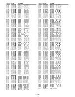
background image

Scanning system : 

PAL standard (625 TV lines, 25 frames/sec.)

Interlace : 

PLL 2:1 interlace

Image device : 

1/3 inch solid state image device CCD

Picture elements : 

795 (Horizontal) x 596 (Vertical)

Effective picture elements : 

752 (Horizontal) x 582 (Vertical)

Synchronizing system : 

Internal sync, Line lock manually switchable

Resolution : 

520 TV lines horizontally, 400 TV lines vertically

Video output level : 

1.0 Vp-p/75 

, composite

Video S/N ratio : 

More than 48 dB

Minimum required illumination : 

Approx. 0.3 lux with a F 1.2 lens (AGC, HI)

(incandescent lighting)                

Approx. 0.6 lux with a F 1.2 lens (AGC, NORM)

Backlight compensation : 

Manual MULT/CENT/OFF switching

                                             (Active when using an auto-iris lens)

Iris function : 

AI/EI selectable by switches (Electronic shutter)

Electronic iris range : 

0.6 lux to 50,000 lux (F1.2, lens)

Electric shutter : 

7 speeds, selectable by switches: (1/50, 1/120, 1/500,

  1/1000, 1/2000, 1/4000, 1/10000 sec.)

Flange-back : 

12.5 mm 

±

 0.5 mm

White balance : 

ATW/Manual switching

Lens mount : 

CS mount

AGC : 

HI/NORM

Environmental conditions : 

Temperature: -10 

°

C ~ + 50 

°

C


 Humidity: less than 90 % (no condensation)

Power supply : 

24 V AC, 50 Hz

Power consumption

 : Approx. 2.8 W (with auto iris lens)

                                      Approx. 2.1 W (without auto iris lens)

Weight : 

Approx. 310 g (without lens)

Dimensions : 

56 (W) mm x 45 (H) mm x 109 (D) mm
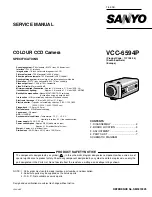
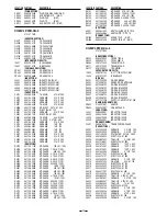
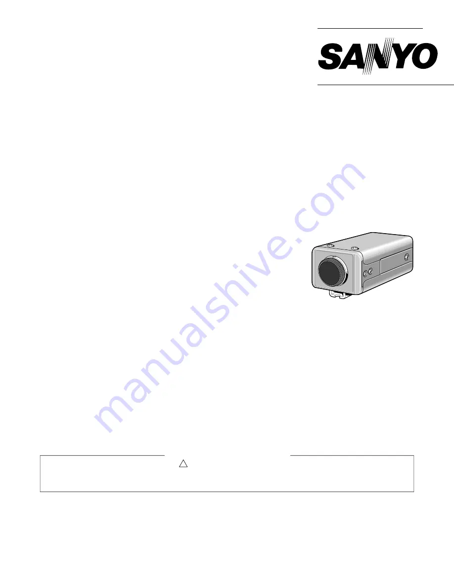
SERVICE MANUAL

COLOUR CCD Camera

VCC-6594P

(Product Code : 117 108 04)
(South East Asia)
(Europe)

FILE NO.

REFERENCE No. SM5310325

L53H4/XE

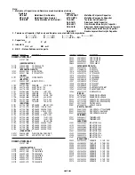
NOTE : 1. Parts order must contain model number, part number, and description.
             2. Substitute parts may be supplied as the service parts.
             3. N. S. P. : Not available as service parts.

Design and specification are subject to change without notice.

The components designated by a symbol (   !   ) in this schematic diagram designates components whose value are of

special significance to product safety. Should any component designated by a symbol need to be replaced, use only the

part designated in the Parts List. Do not deviate from the resistance, wattage, and voltage ratings shown.

PRODUCT SAFETY NOTICE
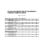
CONTENTS

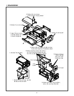
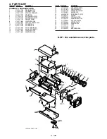
1. DISASSEMBLY ....................................2
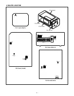
2. BOARD LOCATION ............................. 3
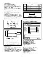
3. ADJUSTMENT ..................................... 4
4. PARTS LIST .........................................7
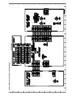
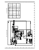
SCHEMATIC DIAGRAM

SPECIFICATIONS

Summary of Contents for VCC-6594P

Page 1: ...al switching Lens mount CS mount AGC HI NORM Environmental conditions Temperature 10 C 50 C Humidity less than 90 no condensation Power supply 24 V AC 50 Hz Power consumption Approx 2 8 W with auto iris lens Approx 2 1 W without auto iris lens Weight Approx 310 g without lens Dimensions 56 W mm x 45 H mm x 109 D mm SERVICE MANUAL COLOUR CCD Camera VCC 6594P Product Code 117 108 04 South East Asia ...

Page 2: ...t and pull out the bottom cabinet 5 Remove the front panel 7 Remove the four screws and then disconnect the connector 8 Remove the five screws then remove the CA 2 CA 3 board assemblies and the FPC and disconnect the connector 9 Remove the five screws and then remove the lens mount bracket 10 Remove the two screws and then remove the CA 1 board assembly CA 3 board CA 4 board CA 2 board CA 1 board ...

Page 3: ...N CA 2 board CA 4 board CA 3 board CA 1 board TP401 S3002 ON S3001 CA 1 board Side B CA 3 board Side A CA 4 board Side B TP103 TP403 VR403 VR302VR303 VR301 DC VIDEO CT232 TP232 CA 2 board Side B CT221 TP221 VR402 Side A ...

Page 4: ...6 Ground test point are TP103 CA 1 and TP401 CA 4 7 Set the distance from the subject to about 60 cm and adjust the camera position so that the picture frame size becomes as shown below when performing the adjustment with the gray scale chart ITE gray scale chart γ 0 45 8 Apply 24 V AC to the 24 V AC terminal on the camera 3 2 PREPARATION 1 Install the adjustment software VHJ 0133 in a computer ru...

Page 5: ... screen Measuring location VIDEO OUT Measuring equipment Oscilloscope Subject Gray scale chart Adjusting method 1 Click the adjustment software installed from the personal computer and the adjustment window will be displayed 2 Display the grayscale chart on full screen 3 Gradually move the lens aperture from the CLOSE side to the OPEN side and secure the aperture at the point where the AGC starts ...

Page 6: ...e gray scale chart on full screen 4 Turn the VR301 to the right so that the white level is maxi mum 5 Turn the VR301 to the left so that the output level is 750 10 mVp p 3 11 Line Phase Adjustment Adjustment location S3002 9 CA 3 VR402 CA 4 Measuring location VIDEO OUT 24 V AC GND terminals Measuring equipment Oscilloscope Subject Attach the lens cap Adjusting method 1 Connect the camera to a 24 V...

Page 7: ...11 126 1404 SCR S TPG BIN 2X4 13 411 023 4201 SCR S TPG PAN 3X10 14 613 197 1820 COMPL PWB CA 2 15 613 197 1837 COMPL PWB CA 3 16 411 167 1302 SCR S TPG BIN 2X7A 17 613 197 1813 COMPL PWB CA 1 18 613 194 1199 SPACER INSULATOR 19 613 194 2813 HOLDER CCD 20 409 498 2105 IC ICX259AK 7 IC101 21 613 188 0771 SPACER 22 645 050 7496 OPTICAL FILTER 23 613 194 2707 HOUSING CRYSTAL 24 411 125 8503 SCR PAN P...

Page 8: ...4 401 105 7909 MT GLAZE 0 000 ZA 1 16W CONNECTORS CN101 645 028 6025 PLUG COAXIAL CABL N S P CN102 645 007 7074 SOCKET FPC 20P N S P COMPL PWB CA 2 613 197 1820 SEMICONDUCTORS Q2001 405 092 4101 TR 2SC4081 R Q2101 405 137 2000 TR 2SA1576A R Q2102 405 092 4101 TR 2SC4081 R Q2103 405 137 2000 TR 2SA1576A R Q2104 405 092 4101 TR 2SC4081 R Q2106 405 092 4101 TR 2SC4081 R Q2107 405 092 4101 TR 2SC4081 ...

Page 9: ... JA 1 16W R2102 401 105 0504 MT GLAZE 1K JA 1 16W R2103 401 105 0504 MT GLAZE 1K JA 1 16W R2104 401 105 2904 MT GLAZE 22K JA 1 16W R2105 401 105 4205 MT GLAZE 33K JA 1 16W R2107 401 105 0504 MT GLAZE 1K JA 1 16W R2109 401 105 0504 MT GLAZE 1K JA 1 16W R2110 401 105 4106 MT GALZE 3 3K JA 1 16W R2112 401 105 1501 MT GLAZE 1 5K JA 1 16W R2113 401 105 5400 MT GLAZE 47K JA 1 16W R2114 401 105 5400 MT G...

Page 10: ...MT GLAZE 0 000 ZA 1 16W R3114 401 105 2003 MT GLAZE 1 8K JA 1 16W R3121 401 105 5301 MT GLAZE 4 7K JA 1 16W R3122 401 105 0504 MT GLAZE 1K JA 1 16W R3123 401 105 5400 MT GLAZE 47K JA 1 16W R3131 401 105 5301 MT GLAZE 4 7K JA 1 16W R3132 401 105 0702 MT GLAZE 100K JA 1 16W R3133 401 105 5301 MT GLAZE 4 7K JA 1 16W R3134 401 105 7909 MT GLAZE 0 000 ZA 1 16W R3135 401 105 4205 MT GLAZE 33K JA 1 16W R...

Page 11: ...0 401 105 0702 MT GLAZE 100K JA 1 16W R4021 401 105 0702 MT GLAZE 100K JA 1 16W R4022 401 105 6001 MT GLAZE 5 6K JA 1 16W R4023 401 105 4205 MT GLAZE 33K JA 1 16W R4024 401 105 1600 MT GLAZE 15K JA 1 16W R4025 401 105 0603 MT GLAZE 10K JA 1 16W R4026 401 105 7909 MT GLAZE 0 000 ZA 1 16W R4027 401 105 6001 MT GLAZE 5 6K JA 1 16W R4028 401 105 0504 MT GLAZE 1K JA 1 16W R4029 401 105 0405 MT GLAZE 10...

Page 12: ...Oct 01 SANYO Electric Co Ltd Osaka Japan ...

Page 13: ...NG C1 OVERALL CIRCUIT BLOCK DIAGRAM C2 CA 1 CIRCUIT WAVEFORMS CA 1 CIRCUIT C3 IC101 IC102 IC103 IC201 IC211 BLOCK DIAGRAMS C4 CA 2 CIRCUIT WAVEFORMS CA 2 CIRCUIT C5 CA 3 CIRCUIT C6 CA 3 CIRCUIT WAVEFORM CA 4 CIRCUIT C7 PRINTED WIRING BOARDS P W B CA 1 BOARD SIDE A B C8 CA 2 BOARD SIDE A B CA 3 BOARD SIDE A B C9 CA 4 BOARD SIDE A B ...

Page 14: ...OSE VALUE ARE OF SPECIAL SIGNIFICANCE TO PRODUCT SAFETY SHOULD ANY COMPONENT DESIGNATED BY A SYMBOL NEED TO BE REPLACED USE ONLY THE PART DESIGNATED IN THE PARTS LIST DO NOT DEVIATE FROM THE RESISTANCE WATTAGE AND VOLT AGE RATINGS SHOWN PAL C EX EXPLANATORY NOTES EXAMPLES Resistor 10K 1 16J means 10kilo ohm 5 1 16watt max 1M 1 10K means 1mega ohm 10 1 10watt max Capacitor 0 047 F means 0 047micro ...

Page 15: ...A B C D E F G H I J K 1 2 3 4 5 6 7 8 9 10 11 12 13 14 15 16 17 18 19 A B C D E F G H I J K C1 OVERALL WIRING BLOCK DIAGRAM CIRCUIT DIAGRAMS OVERALL WIRING ...

Page 16: ...J K C2 OVERALL CIRCUIT BLOCK DIAGRAM WAVEFORM TEST LOCATION WAVEFORM TEST LOCATION IC101 1 5V div 20µs div V4 IC101 2 5V div 20µs div V3 IC101 3 5V div 20µs div V2 IC101 15 16 2V div 50ns div H1 H2 IC101 4 5V div 20µs div V1 IC101 13 2V div 50ns div RG WF CA1 L53X4XE CA 1 CIRCUIT WAVEFORMS ...

Page 17: ...A B C D E F G H I J K 1 2 3 4 5 6 7 8 9 10 11 12 13 14 15 16 17 18 19 A B C D E F G H I J K C3 CA 1 CIRCUIT ...

Page 18: ...MC CKI2 PCOVD Data pass SG2 1 2 3 4 5 6 7 8 9 10 11 12 13 14 15 16 NOTE NOTE PHOTO SENSOR V OUT V SS V GG GND 1 2 3 4 V DD GND SUB V L RG 1 1 2 H RERISTER Cy Ye Cy Ye Mg G Mg G Cy Ye Cy Ye G Mg G Mg Cy Ye Cy Ye Mg G Mg G V RERISTER V RERISTER V RERISTER V RERISTER Charge Pump CPP3 V H DCIN XSHT XV2 XV1 XSG1 XV3 XSG2 XV4 CPP1 CPP2 DCOUT VSHT V L V M 2 3 4 5 6 7 8 9 10 11 12 13 14 15 16 17 18 19 20 ...

Page 19: ...A B C D E F G H I J K 1 2 3 4 5 6 7 8 9 10 11 12 13 14 15 16 17 18 19 A B C D E F G H I J K C5 CA 2 CIRCUIT ...

Page 20: ... C D E F G H I J K 1 2 3 4 5 6 7 8 9 10 11 12 13 14 15 16 17 18 19 A B C D E F G H I J K C6 CA 3 CIRCUIT WAVEFORM TEST LOCATION S3001 4 0 5V div 2ms div VIDEO TYPE LENS WF CA3 L53X4US CA 3 CIRCUIT WAVEFORM ...

Page 21: ...A B C D E F G H I J K 1 2 3 4 5 6 7 8 9 10 11 12 13 14 15 16 17 18 19 A B C D E F G H I J K C7 CA 4 CIRCUIT ...

Page 22: ...A B C D E F G H I J K 1 2 3 4 5 6 7 8 9 10 11 12 13 14 15 16 17 18 19 A B C D E F G H I J K C8 CA 1 BOARD SIDE A CA 1 BOARD SIDE B CA 2 BOARD SIDE A CA 2 BOARD SIDE B PRINTED WIRING BOARDS P W B ...

Page 23: ...A B C D E F G H I J K 1 2 3 4 5 6 7 8 9 10 11 12 13 14 15 16 17 18 19 A B C D E F G H I J K C9 CA 3 BOARD SIDE A CA 3 BOARD SIDE B CA 4 BOARD SIDE A CA 4 BOARD SIDE B ...

Reviews: