background image

– 17 –

1. Shaft cover batt

2. Spring cover batt

3. Compl, cover batt

4. Spacer holder joint

5. Two screws 1.7 x 4

6. Screw 1.7 x 2.5

7. Two screws 1.7 x 3.5

8. Cover joint inner

9. Two screws 1.7 x 3.5

10. Earth joint LCD

11. Pull the LCD from the body.

12. Holder LCD

13. Screw 1.7 x 3.5

14. Holder joint base

15. Two screws 1.7 x 2.5

16. Two screws 1.7 x 3.5

17. Two screws 1.7 x 4.5

18. Cover LCD back

19. Spacer mic 2

20. Dec LCD top

21. Four screws 1.7 x 2

22. Earth LCD A

23. Holder joint R

24. Holder joint L

25. Pull the assy joint

      from the LCD.

26. Four screws 1.7 x 3

27. Cover LCD inner

28. FPC

29. FPC

30. Four screws 1.7 x 2.5

31. FPC

32. LCD

33. Three screws 1.7 x 2

34. VF1 board

35. Holder LCD

36. Gasket LCD

37. Cover LCD front

38. Assy joint

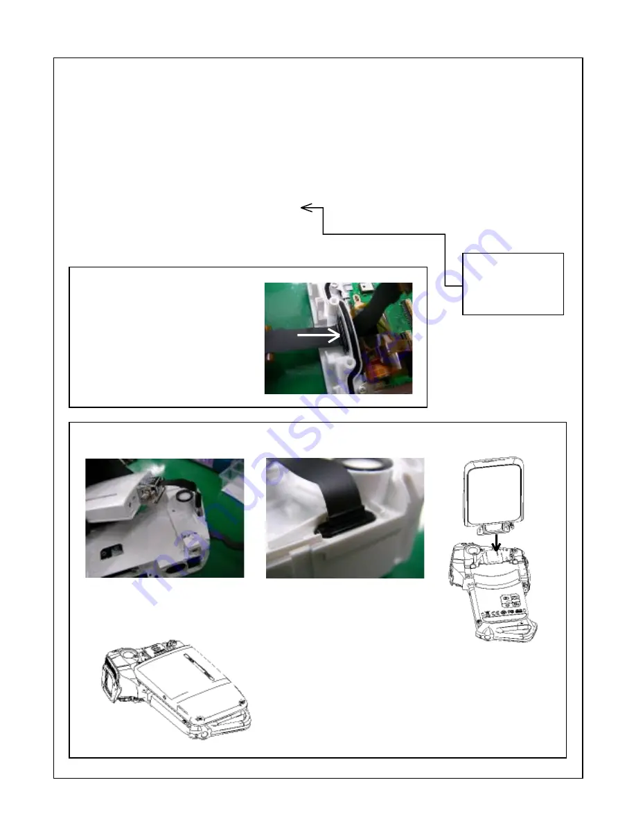
Installing the ASSY JOINT (RUBBER)

to the COVER LCD FRONT (step 28)

Install so that the rubber will not come out.

Installing the LCD to the CABI RIGHT (step 11)

1. Insert the FPC of the LCD into the

CABI RIGHT.

2. Install the rubber of the ASSY JOINT

to the cabinet.

3. Install the LCD joint

to the cabinet.

4. After installing, close the LCD.

When reassembling

The air leak test should

be carried out between

steps 20 and 21.

Summary of Contents for VPC-CA8EXBK

Page 1: ... requested to use RoHS compliant parts for maintenance or repair You are requested to use lead free solder This product has been manufactured using lead free solder Be sure to follow the warning given on page 2 when carrying out repair work VPC E2W Product Code 168 148 02 U S A Canada VPC CA8EXW Product Code 168 148 03 Europe U K South America China Australia Hong Kong Russia Middle East Africa Ge...

Page 2: ...0 C 662 F or less for chip compo nents to 380 C 716 F for lead wires and similar and to 420 C 788 F when installing and removing shield plates The tip of the soldering iron should have a C cut shape or a driver shape so that it can contact the circuit board as flat or in a line as much as possible Solder Use solder with the metal content and composition ratio by weight given in the table below Do ...

Page 3: ...The electric charges which are generated when each pixel is optically converted are in turn converted into signal voltages by the FD amplifier and they are then transmitted by the built in H driver and V driver The signals are sampled and ampli fied by the CDS and PGA circuits at the point they are output and then they are AD converted and output The output uses the 12 bit parallel interface 1 2 3...

Page 4: ...At this time correction of the lens distortion which is a characteristic of wide angle lenses is carried out After AWB and γ processing are carried out a matrix is generated and aperture correction is carried out for the Y signal and the data is then compressed by JPEG and is then written to card memory SD card When the data is to be output to an external device it is taken data from the memory an...

Page 5: ... stepping motor for focusing operation Detection of the standard focusing positions is carried out by photointerruptor F_SENSE inside the lens block 4 2 Zoom drive The 16 bit serial data signals LENS_SD and LENS_SCLK and LENS_EN which are output from the ASIC IC101 are used to drive ZOOM A ZOOM A ZOOM B and ZOOM B by the motor driver IC IC951 and are then used to microstep drive the stepping motor...

Page 6: ...1 all output is turned off To reset momentarily set the control sig nal P ON to repeat control or temporarily disconnect the input power supply 3 Motor System Power Output BOOST 5 3 V is output Feedback for the 5 3 V output is pro vided to the switching controller Pin B7 of IC501 so that PWM control can be carried out 4 Digital 3 25 V Power Output VDD3 is output Feedback for the VDD3 is provided t...

Page 7: ...mer 1 5 Rectifier circuit The high voltage alternating current which is generated at the secondary side of T5401 is rectified to produce a high voltage direct current and is accumulated at electrolytic ca pacitor C5412 1 6 Charge monitoring circuit The functions programmed in the IC541 monitor oscillations and estimate the charging voltage If the voltage exceeds the rated value charging automatica...

Page 8: ...p battery charge control L charge Strobo condensor charge done detection H L charge done Hot line request from ASIC Test mode terminal L starting up test mode VDD Red LED H lighting Green LED H lighting OneNAND flash reset L reset LCD backlight ON OFF signal H backlight ON System reset MRST ASIC PLL ON OFF control Debugger terminal BOOT Lo output normal starting up Hi z Key input PLAY L input VSYN...

Page 9: ...ACK connection detection L connection VSS1 UNREG SY I Camera power voltage input 61 62 XOUT O Main clock oscillation terminal 4 MHz VDD1 VDD 51 KEY_POWER I Key input POWER 52 KEY_2ND I Key input 2nd SHUTTER 55 56 RESET I Microprocessor reset input L reset 57 XCIN I Sub clock oscillation terminal 32 768 kHz 58 XCOUT O Sub clock oscillation terminal 32 768 kHz 60 XIN I Main clock oscillation termina...

Page 10: ...microprocessor only carries out clock counting and waits in standby for the battery to be attached again When a switch is operated the 8 bit microprocessor supplies power to the system as required The 8 bit microprocessor first sets the P ON signal at pin 40 to high and then turns on the DC DC converter After this low signal is output from pin 17 so that the ASIC is set to the reset condition Afte...

Page 11: ... be supplied as single parts Summary of waterproof maintenance parts kit Parts name COMPL MENT KIT SV 114 Parts code 636 110 2131 NO DESCRIPTION 1 2 3 GASKET CABINET SG114 J 4 1 NUMBER 5 2 SPACER MIC2 SG114 J 1 GASKET LCD SG114 J 6 PAD BATTERY SG114 J 1 ADHESIVE COV BATT A SG114 1 1 ADHESIVE COV BATT B SG114 7 ADHESIVE COV BATT D SG114 1 CABINET LCD COVER BATTERY PARTS NO 6361040174 6361073998 636...

Page 12: ...8 29 30 31 a b c 32 33 11 NOTE Discharge a strobe capacitor with the discharge jig VJ8 0188 for electric shock prevention When assembling tighten the screws order a b c d e f When assembling assemble order A B C When assembling assemble order A B C 2 1 REMOVAL OF CABI LEFT AND LENS When assembling assemble order a b c ...

Page 13: ...r 28 FPC 29 FPC 30 Lens assy 31 Three screws 1 4 x 4 5 32 Heat sink CMOS 2 33 Assy flexible pwb CA1 When reassembling The air leak test should be carried out between steps 8 and 9 At this time the battery cover should be closed and locked approximately 45 degrees ASSY FPC GASKET installing method between steps 8 and 9 on page 12 and 13 Tilt the LCD to approximately 45 degrees Next push the ASSY FP...

Page 14: ... 12 13 14 Installing the gasket cabinet step 13 on page 12 Install from directly above in the order of the numbers so that the gasket is not twisted Do not touch the solder Lead wire of speaker dressing method step 21 on page 12 ...

Page 15: ...r 16 Spacer ST1 17 Two screws 1 7 x 2 18 Connector 19 ST1 board 20 Remove the solder 21 Spacer H flash B 22 Assy lamp 23 Screw 1 7 x 2 24 Holder CP1 25 Screw 1 7 x 2 26 Holder CP1 2 27 Two screws 1 7 x 6 28 Assy holder strap 29 Gasket strap 30 Screw 1 7 x 3 5 16 3 4 1 31 Spring lock lever 32 Lever batt lock When assembling The air leak test should be carried out between steps 26 and 27 At this tim...

Page 16: ... E D D C C F H G F M H 2 3 REMOVAL OF LCD AND VF1 BOARD When assembling tighten the screws order A B C When assembling tighten the screws order a b c d When assembling tighten the screws order A B 3 4 2 1 Installing the gasket LCD step 36 Install from directly above in the order of the numbers so that the FPC is not twisted When assembling tighten the screws order A B ...

Page 17: ...oint R 24 Holder joint L 25 Pull the assy joint from the LCD 26 Four screws 1 7 x 3 27 Cover LCD inner 28 FPC 29 FPC 30 Four screws 1 7 x 2 5 31 FPC 32 LCD 33 Three screws 1 7 x 2 34 VF1 board 35 Holder LCD 36 Gasket LCD 37 Cover LCD front 38 Assy joint Installing the ASSY JOINT RUBBER to the COVER LCD FRONT step 28 Install so that the rubber will not come out Installing the LCD to the CABI RIGHT ...

Page 18: ... 18 2 4 BOARD LOCATION CA1 board CP1 board ST1 board VF1 board ...

Page 19: ...color temperature to 3100 20 K and luminosity to 900 20 cd m2 Be careful of handling the lump and its circumference are high temperature during use and after power off for a while 4 Computer screen during adjustment 3 5 Connecting the camera to the computer This camera requires a DC adaptor sold separately in order to use an AC adaptor 1 Insert the DC adaptor to the camera 2 Insert the AC adaptor ...

Page 20: ... focus2 100 100 focus3 100 200 focus4 200 lens_error 0 0 g 255 0 o 255 3 6 The adjustment item which in necessary in part exchange COMPL PWB CP 1 Lens Adjustment AWB Adjustment CCD White Point Defect Detect Adjustment CCD Black Point And White Point Defect Detect Adjustment In Lighted Factory Cord Setting USB storage information registration Language Setting COMPL PWB ST 1 COMPL PWB VF 1 Reset Set...

Page 21: ...1 s2 s3 s4 s5 Adjustment values other than the above are irrelevant 3 CCD White Point Defect Detect Adjustment Preparation POWER switch ON Adjustment method 1 Double click on the DscCalDi exe 2 Select CCD Defect on the LCD Test and click the Yes 3 After the adjustment is completed OK will display 4 Click the OK 4 CCD Black Point And White Point Defect Detect Adjustment In Lighted Preparation POWER...

Page 22: ...f the distributed firmware For XX X enter the name of the circuit board containing the firmware 2 The firmware is distributed by e mail in self extracting archive format Change the extension of the distributed file to EXE and save it in your preferred folder 3 When you double click the saved file the firmware binary file will be saved in the same folder 4 The firmware must not be distributed witho...

Page 23: ...PC CA8EXW VPC CA8GXW VPC CA8EXBL VPC CA8GXBL VPC CA8EXBK VPC CA8GXBK E2 VPC E2W VPC E2BL VPC E2BK Serial Rev 1 00 4 Check the Serial in the above USB storage data If the displayed value is different from the serial number printed on the base of the camera enter the number on the base of the camera Then click the Set button 5 Next check VID PID and Rev entries in the USB storage data If any of them...

Page 24: ...CHECK UNIT SW IC101 E1 G5 PAON1 PAON2 CHECK IC101 IC301 PWA BLOCK CAA BLOCK SERIAL COMMUNICATION CHECK IC301 CP1 DMA BLOCK CHECK CP1 DMA BLOCK TAKING INOPERATIVE HIGH LOW LOW LOW NO LOW HIGH HIGH HIGH YES YES HIGH OK NO LOW NG NO PICTURE MAIN CLOCK FOR SYSTEM OPERATION NO OPERATION IF ABSENT CHECK X1102 OSCILLATOR IC101 AB18 AK20 CHECK OSCILLATION IC301 63 64 ASIC_SO ASIC_SI CHECK SOLDERING OF MEM...

Page 25: ... 25 MEMO ...

Page 26: ...5841 STRAP SG114 J 2 636 104 5834 CASESOFT SG114 J 3 645 087 1818 CABLE DSC USB 4 645 087 1825 CABLE DSC A V 5 645 093 9624 BATTERY CHARGER VPC E2BK VPC E2W VPC E2BL 6 645 083 6787 CORD POWER 1 2MK VPC CA8EXW VPC CA8EXBL VPC CA8EXBK 7 645 093 9617 BATTERY CHARGER EXCEPTVPC E2BK VPC E2W VPC E2BL 8 645 089 8990 BATTERY RECHARGE LI ION 9 6361151306 DISC DVD XSD G219 EX N S P EXCEPTVPC E2W VPC E2BL VP...

Page 27: ...2 7 1 1 2 3 3 4 5 5 6 6 7 7 8 8 9 ACCESSORIES ...

Page 28: ...VPC CA8EXBK VPC CA8GXBK 28 6361151016 DEC RIGHT SG219 J3 VPC E2BK VPC CA8EXBK VPC CA8GXBK 29 636 104 0068 DEC GRIP SG114 J VPC E2BL VPC CA8EXBL VPC CA8GXBL 29 6361150835 DEC GRIP SG219 J VPC E2W VPC CA8EXW VPC CA8GXW 29 6361150842 DEC GRIP SG219 J3 VPC E2BK VPC CA8EXBK VPC CA8GXBK 30 636 109 3774 SPACER FPC GRIP2 SG114 J 31 636 104 3724 BUTTON MENU SG114 J VPC E2BL VPC CA8EXBL VPC CA8GXBL 31 63611...

Page 29: ... D C D 111 111 51 50 49 38 39 40 111 54 110 5 48 46 48 53 52 47 43 42 41 16 17 11 12 14 15 18 9 7 103 8 2 3 1 4 101 6 102 102 5 10 13 23 22 21 20 19 21 105 106 105 27 26 28 105 105 104 25 103 103 103 29 107 30 31 103 108 35 33 37 32 36 34 106 103 24 109 45 44 CABINET AND CHASSIS PARTS 1 ...

Page 30: ...PTVPC E2BK VPC CA8EXBK VPC CA8GXBK 77 6361177689 COMPL BUTT BACK SV 219J3 VPC E2BK VPC CA8EXBK VPC CA8GXBK 78 6361177702 ASSY JOINT SV SG219 79 636 104 0570 DEC MIC SG114 J 80 6361150972 COVER LCD BACK SG219 J VPC E2W VPC CA8EXW VPC CA8GXW 80 6361150989 COVER LCD BACK SG219 J2 VPC E2BL VPC CA8EXBL VPC CA8GXBL 80 6361150996 COVER LCD BACK SG219 J3 VPC E2BK VPC CA8EXBK VPC CA8GXBK 81 636 104 0167 DE...

Page 31: ...56 108 112 108 58 112 112 62 63 113 65 64 112 61 60 114 67 68 69 101 59 66 9 69 70 70 72 64 113 106 106 106 106 106 104 65 74 74 75 77 76 73 71 55 91 119 89 88 87 86 85 118 118 118 84 104 104 106 106 79 115 115 81 80 81 118 117 117 116 116 83 83 116 116 82 CABINET AND CHASSIS PARTS 2 ...

Page 32: ...410 655 7604 IC LC87F2924BUFL64TBM E BGA N S P IC302 309 582 6203 IC BD4289FVM IC501 410 644 3303 IC UPD168803FC AN2 A BGA N S P IC502 409 686 6205 IC SC4624MLT IC503 409 691 1400 IC XC9235A28CE IC902 409 690 7403 IC TC7SG126FE IC911 409 690 0909 IC TK70628HC G IC913 409 690 0909 IC TK70628HC G IC914 409 690 7502 IC TC7SP3125TU IC951 409 680 0506 IC BU2233GU BGA N S P IC971 309 646 8709 IC AK7331 ...

Page 33: ...601 CERAMIC 0 22U K 6 3V C9008 303 381 8109 CERAMIC 1U K 6 3V C9009 303 419 8903 CERAMIC 10U M 6 3V C9012 303 276 1307 CERAMIC 1000P K 50V C9013 303 338 0309 CERAMIC 0 1U K 10V C9014 303 338 0309 CERAMIC 0 1U K 10V C9015 303 276 1307 CERAMIC 1000P K 50V C9016 303 276 1307 CERAMIC 1000P K 50V C9017 303 276 1307 CERAMIC 1000P K 50V C9019 303 338 0309 CERAMIC 0 1U K 10V C9023 303 384 6409 CERAMIC 4 7...

Page 34: ...R9505 301 314 0503 MT FILM 22 FD 1 6W R9506 301 314 0503 MT FILM 22 FD 1 6W R9701 301 257 4101 MT GLAZE 100K DC 1 16W R9702 301 257 4101 MT GLAZE 100K DC 1 16W R9703 301 262 1904 MT GLAZE 6 8K DC 1 16W R9704 301 262 1607 MT GLAZE 2 2K DC 1 16W R9705 301 262 2307 MT GLAZE 1 0K DC 1 16W R9706 301 224 9504 MT GLAZE 2 2K JA 1 16W R9707 301 257 4101 MT GLAZE 100K DC 1 16W R9708 301 225 0500 MT GLAZE 33...

Page 35: ...ERAMIC 0 1U K 10V N S P C9102 303 338 0309 CERAMIC 0 1U K 10V N S P C9103 303 338 0309 CERAMIC 0 1U K 10V N S P C9104 303 338 0309 CERAMIC 0 1U K 10V N S P C9105 303 338 0309 CERAMIC 0 1U K 10V N S P C9106 303 338 0309 CERAMIC 0 1U K 10V N S P C9107 303 338 0309 CERAMIC 0 1U K 10V N S P C9108 303 439 8402 CERAMIC 2 2U K 6 3V N S P C9109 303 338 0309 CERAMIC 0 1U K 10V N S P C9110 303 338 0309 CERA...

Page 36: ...TROBE CIRCUIT C7 SYSTEM CONTROL CUIRCUIT C8 CIRCUIT DIAGRAMS CIRCUIT WAVEFORMS C8 CP1 BOARD DMA MAIN C9 CP1 BOARD TCA LENS C14 CP1 BOARD SYA SYSTEM CONTROL C15 CP1 BOARD PWA POWER C16 CP1 BOARD CAA CAMERA C17 CA1 BOARD IMAGE SENSOR C18 VF1 BOARD LCD CONNECTOR MIC C19 ST1 BOARD STROBE C20 PRINTED WIRING BOARDS P W B CP1 P W B SIDE A B C21 VF1 P W B SIDE A B C22 ST1 P W B SIDE A B C22 CA1 P W B SIDE...

Page 37: ...IATE FROM THE RESISTANCE WATTAGE AND VOLT AGE RATINGS SHOWN EXPLANATORY NOTES EXAMPLES Resistor 10K 1 16J means 10kilo ohm 5 1 16watt max 1M 1 10K means 1mega ohm 10 1 10watt max Capacitor 0 047 F means 0 047micro farad Ftype Electrolytic capacitor 10 16 means 10micro farad 16volt max Inductor 330 J means 330micro henry 5 470 K means 470micro henry 10 No description J or K means 5 Figure of printe...

Page 38: ... MR_OPEN 4 PLAY 11 GND 5 GND 12 GND 6 POWER 13 GND 7 GND 8 AL3 2V 9 GND 1 GND 2 GND 3 GND Z1 Z2 CN901 10 GPI3 4 VDDPLL 11 GPI2 5 VDDIO 12 SHUTTER 6 VDDIO 13 FRAME_VALID 7 GND 14 LINE_VALID 8 GPI0 15 D_GND 9 GPI1 16 PIXCLK 17 D_GND 18 EXTCLK 19 D_GND 20 A_GND 1 D_GND 2 VDD_1_8 3 VDD_1_8_ 21 VAA_2_8 22 VAA_2_8 23 VAAPIX_A 24 A_GND 25 VAAPIX_B 26 A_GND 27 D_GND 28 RESET_BAR 29 SCL 30 SDATA 31 FLASH 3...

Page 39: ...ENSOR IC911 MICROPHONE R MICROPHONE L FPC LCD 2 5inch TPO SD CARD FPC FPC FPC B to B B to B IC301 8bit MICRO PROCESSOR IC302 BATTERY BACKUP BATTERY TERMINAL IC501 SWITCHING CONTROL IC541 STROBE CHARGE FLASH REFLECTOR TRIG TRANS LENS UNIT FPC SWITCH UNIT LED MAIN CAPACITOR FPC X1102 48 000MHz X3002 32 768KHz SWITCH UNIT LED AV USB 10 pin ARM CPU VOUT CN141 CN951 CN105 CN110 CN103 CN301 CN901 CN911 ...

Page 40: ... HALL OUT1 IRISPWM HIREG OUT PWM OUT DRIVE DRIVE HALL IN HALL IN HALL OUT HALL OUT Z_SENSE 6 F_SENSE ZOOM_PI FOCUS_PI IC971 AK7331 IRIS CONTROLLER IC951 BU2233GU LENS DRIVER ZOOM VCC FOCUS VCC CN951 LENS_BLOCK E9 H2 D2 E3 F1 F2 G2 G1 H1 H10 F9 F8 F10 16 17 13 15 22 14 9 12 11 10 4 5 8 2 3 PILED FPIOUT IC101 L4pin SOUT F3 RXD0 IC101 AF23pin ZPIOUT IC101 H2pin HALL OUT2 BOOST5 3V MVCC12 MVCC34 MVCC5...

Page 41: ...22 AK23 H26 G26 L29 L30 K26 N10 P7 U3 J12 J11 K12 K11 F3 CN103 FPC VF1 BOARD CN141 SD SDDAT 0 3 LMCLK LCDSD LCDEN LCDCK LCDRESET LCDD 1 7 LCDHD LCDVD SDCLK SDCMD SDDET SDWP CN301 FPC CN105 B to B SW UNIT ST1 BOARD PAON1 PAON2 MRST PLLEN ZSREQ ASIC_SCK ASIC_SDI ASIC_SDO COMREQ FLCTL YOUT 4 XO XI AUD_256FS BCLK DACDAT LRCLK ADCDAT AMCLK AUDEN AUDSD AUDCK 18 22 64 63 1 50 18 17 27 14 13 11 12 17 8 10...

Page 42: ...05 VDD1 0 PON2 VAA2 8 PAON2 UPD168803FC AN2 E1 IC501 SWITCHING CONTROL E7 H5 G5 H6 G6 17 19 14 6 3 4 E1 E2 LOUT 31 32 LOUTA 21 22 LOUTB 21 22 E5 SHDNB7 B1 B2 C1 C2 F6 CTL1 D6 SHDNB23 SW Q5003 UNREGST SW3 2V FLCTL CHG ZCHGDONE AL3 2V TO DMA C5412 C5401 T5401 T5402 D5402 Q5402 POWER FILTER OSCILLATION TRANSFORMER BLOCK RECTIFIER CIRCUIT EMISSION CONTROL CIRCUIT TRIGGER CIRCUIT LIGHT EMITTING ELEMENT...

Page 43: ...2 TO SW UNIT TO DMA TO SW UNIT IC302 BD4289FVM BATTERY BACKUP STANDBY LED SW UNIT AL3 2V KEY_2ND KEY_LEFT KEY_1st KEY_UP TELE ASSY FPC POWER 26 TH301 TEMP SENSOR PON KEY_VREC KEY_SET KEY_RIGHT KEY_MENU ASSY FPC VF1 44 MR_TURN 64 1 UNREGSY NAND_RESET ZCARD ZUSBDET ZAVJACK HOTLINE MRST LCDD0_ZBOOT ZSREQ PLLEN ASIC_SDI ASIC_SDO ASIC_SCK PON BLON ST_CHG ZCHGDONE SW3 2ON BACKUP3 2V SW3 2V Q3004 Q3001 D...

Page 44: ...DRC2 H20 VSS_DDRC2 PLLEN 51 1 16J R1002 BLM15BA330SN1 L1002 1 B C1304 VDD3 10 1AV4J11B7791G CN110 10 LINE_R 4 USB_D 5 S_VIDEO_Y 6 VIDEO 7 S_VIDEO_C 8 LINE_L 9 GND 1 AV_JACK 2 USB_VBUS 3 USB_D Z1 Z2 Z3 Z4 BK1608LM751 1AV4L26B1150G 1608 L1302 UP0431300 Q1302 1 2 3 4 5 6 USBD USBD 220 RB116 1 2 100 1 16J R1051 100 1 16J R1052 220 1 16J R1056 10K 1 16J R1032 220 RB116 7 8 220 RB116 3 4 VDD1 8 220 RB11...

Page 45: ...AD15 VDD_CORE AD16 VDD_CORE AD17 VDD_CORE AD18 VDD_CORE H23 VDD_DDR1 H24 VDD_DDR1 J23 VDD_DDR1 J24 VDD_DDR1 K24 VDD_DDR1 R23 VDD_DDR1 R24 VDD_DDR1 T23 VDD_DDR1 T24 VDD_DDR1 G14 VDD_DDR2 G15 VDD_DDR2 G21 VDD_DDR2 G22 VDD_DDR2 G23 VDD_DDR2 H14 VDD_DDR2 H15 VDD_DDR2 H21 VDD_DDR2 M20 VDD_DDRC1 N19 VDD_DDRC1 N20 VDD_DDRC1 P20 VDD_DDRC1 R20 VDD_DDRC1 L18 VDD_DDRC2 L19 VDD_DDRC2 L20 VDD_DDRC2 M18 VDD_DDR...

Page 46: ...DQ26 H5 DQ25 H10 DQ9 H11 DQ8 H12 VDDQ H13 VSSQ J1 NC J2 VDDQ J3 VSSQ J4 DQ24 J5 DQM3 J10 WE J11 CAS J12 RAS J13 CS J14 NC K1 NC K2 VSSd K3 VDD K4 DQS3 K5 SA12 K10 VSSd K11 CK K12 CK K13 NC K14 NC L1 NC L2 VSSQ L3 VDDQ L4 BA0 L5 BA1 L10 DQ6 L11 DQ7 L12 VDDQ L13 VSSQ L14 NC M2 VDDQ M3 VSSQ M4 DQM2 M5 DQS2 M10 DQ4 M11 DQ5 M12 VSSQ M13 VDDQ N2 DQ18 N3 DQ19 N4 DQ23 N5 DQ22 N10 OEBo N11 DQ3 N12 DQS0 N13...

Page 47: ... U23 VSS_DDR1 U24 VSS_DDR1 V23 VSS_DDR1 V24 VSS_DDR1 L14 VSS_DDR2 L15 VSS_DDR2 L16 VSS_DDR2 L17 VSS_DDR2 M14 VSS_DDR2 M15 VSS_DDR2 M16 VSS_DDR2 M17 VSS_DDR2 K23 VSS_DDRC1 L23 VSS_DDRC1 M23 VSS_DDRC1 N23 VSS_DDRC1 P23 VSS_DDRC1 H16 VSS_DDRC2 H17 VSS_DDRC2 H18 VSS_DDRC2 H19 VSS_DDRC2 H20 VSS_DDRC2 PLLEN 51 1 16J R1002 BLM15BA330SN1 L1002 220 RB116 1 2 100 1 16J R1051 100 1 16J R1052 220 1 16J R1056 ...

Page 48: ...18 AVSS12D_PLLS1 AG17 AVDD12A_PLLC AG18 AVDD12A_PLLS0 AG19 AVDD12A_PLLS1 AF17 AVSS12A_PLLC AF18 AVSS12A_PLLS0 AF19 AVSS12A_PLLS1 AF27 TEST1 AF26 TEST0 J8 ZSREQ L7 SCK L8 SDI J7 SDO L30 DSCKAP L29 DSCKAN 1 B C1304 VDD3 10 1AV4J11B7791G CN110 10 LINE_R 4 USB_D 5 S_VIDEO_Y 6 VIDEO 7 S_VIDEO_C 8 LINE_L 9 GND 1 AV_JACK 2 USB_VBUS 3 USB_D Z1 Z2 Z3 Z4 BK1608LM751 1AV4L26B1150G 1608 L1302 UP0431300 Q1302 ...

Page 49: ...RESETB G1 SCLK H1 CS J1 NC K1 NC K2 OUT1A K3 OUT1B K4 MGND12 K5 OUT2B K6 OUT4B K7 MGND34 K8 OUT3B K9 OUT3A K10 NC J10 NC H10 IN5A G10 IN7B F10 IN6B E10 SI2 D10 SI3 C10 SO4 B10 NC A10 NC A9 OUT5A A8 OUT5B A7 MGND56 A6 OUT6B A5 MGND7 A4 RNF A3 SENSE A2 VDDAMP B2 NC C2 NC D2 STATE1 E2 STATE3 F2 CLK G2 SDATA H2 MODE J2 NC J3 NC J4 MVCC12 J5 OUT2A J6 NC J7 OUT4A J8 MVCC34 J9 NC H9 NC G9 IN7A F9 IN5B E9...

Page 50: ..._LEFT 31 H7 KEY_RIGHT 32 G8 KEY_SET 33 G7 KEY_VREC 34 F6 VSS3 35 F7 VDD3 36 E7 RDSEL 37 F8 CLK SFW 38 E6 DATA0 SFW 39 E8 PON 40 D8 PON2 41 D7 N C 42 C8 KEY_MENU 43 D6 MR_TURN 44 C7 45 N C D5 46 N C A8 N C 47 B8 48 N C A7 BAT_OFF 49 B7 ZSREQ 50 C6 KEY_POWER 51 B6 KEY_2ND 52 B5 RESET 53 A6 XCIN 54 C5 XCOUT 55 A5 VSS1 56 A4 XIN 57 B4 XOUT 58 A3 VDD1 59 C4 INREGSY 60 B3 ZAV_JACK 61 D4 TH_TEMP 62 A1 AS...

Page 51: ...008 1 2 3 4 5 33 8 V 3 5X2 8 H 2 0 C5302 2 4K 1 16D R5104 100 1 16J R5043 VDD1 8 12K 1 16D R5023 3P CJ 50 C5110 BLON 0 1 B 10 C5006 100K 1 16J R5046 2A32V F88K2R0D3MFFD F5001 1 2 VDD1 0 2 2 B 16 1608 C5071 24K 1 16D R5107 UP03396 Q5005 1 2 3 4 5 2A32V F88K2R0D3MFFD F5002 1 2 LCDAN 1 B 1608 16 C5007 180K 1 16D R5021 VAA2 8 MA21D38 D5301 1 B 1608 16 C5072 4 7 N 1AV4L2MJ4R7NG 3 0X3 0 H 2 0 7E03ND4R7N...

Page 52: ...1 B C9019 CMOS1 8V EXT_CLK PIX_CLK EXT_CLK PIXCLK PIXCLK VAAPIX_B VAAPIX_A CMOS_SDATA CMOS_SCLK CMOS1 8V CMOS1 8V VDDPLL VDDPLL GPI0 GPI1 GPI2 GPI3 EXTCLK EXTCLK_CTL DTC144EM Q9003 VDD3 0 1 B C9004 0 1 16Z R9014 CMOS1 8V TK70628HCL G QTK70628HC GG IC911 1 VCONT 2 GND 3 NP 4 VOUT 5 GND 6 VIN TK70628HCL G IC913 1 VCONT 2 GND 3 NP 4 VOUT 5 GND 6 VIN 0 1 16Z R9007 TC7SP3125TU 2 1X2 0 H 0 75 IC914 1 Vc...

Page 53: ...1 1 D_GND D_GND A_GND A_GND D_GND AVR M1005C080MTAAB VA911 D_GND 0 1 B C9111 QXXAGB037 M IC911 1 DOUT2 2 DOUT1 3 DOUT0 4 VDDPLL 5 EXTCLK 6 DGND 13 PIXCLK 14 VDD 15 SCLK 16 SDATA 17 RESET_BAR 18 VDDIO 25 TEST 26 FLASH 27 SHUTTER 28 FRAME_VALID 29 LINE_VALID 30 DGND 37 VAAPIX 38 VAAPIX 39 AGND 40 VAA 41 PIXGND 42 NC 43 NC 44 DGND 45 DOUT6 46 DOUT5 47 DOUT4 48 DOUT3 7 DOUT7 8 DOUT8 9 DOUT9 10 DOUT10 ...

Page 54: ...D 6 LCDD2 13 LMCLK 7 LCDD3 14 GND 8 LCDD4 15 HD 9 LCDD5 16 VD 17 LCDRESET 18 LCDEN 19 LCDCK 20 LCDSD 1 GND 2 GND 3 VDD3 21 LCD_CA 22 LCD_AN 23 VDD3 24 MR_PANEL_TURN 25 GND 26 AA_GND 27 AA_GND 28 MIC_R 29 MIC_L 30 GND 31 GND Z1 Z2 AA_GND AA_GND AA_GND AA_GND AA_GND AA_GND AA_GND 39 1AV4J11VR391G CN171 10 DIN3 4 SCL 11 DIN2 5 SDA 12 DIN1 6 DIN7 13 DIN0 7 DIN6 14 DCLK 8 DIN5 15 HD 9 DIN4 16 VD 17 VCC...

Page 55: ...10 CHG 11 PGND 12 PGND 13 NC 14 NC 15 VBAT 16 NC Z1 AWG28 2 2X1 5 JW541 PINK 1 XAN AWG28 2 2X1 5 JW542 BLACK 1 XKT 0 018 350B 3216 C5410 FV02R80TP D5402 20 1AV4J11JX200G CN541 10 BOOST5 3V 4 ZCHGDONE 11 GND 5 CHG 12 GND 6 FLCTL 13 GND 7 SW3 2V 14 GND 8 BOOST5 3V 15 GND 9 BOOST5 3V 16 UNREGST 17 UNREGST 18 UNREGST 19 UNREGST 20 UNREGST 1 AL3 2V 2 AL3 2V 3 AL3 2V 40 300 E CEXAG646400AN 300FW40A7 5X2...

Page 56: ...01 RB304 RB305 RB306 X3001 X3002 RB311 RB312 F5001 F5002 F5003 F5004 IC302 IC181 CL102 CL108 CL109 CL301 CL302 CL110 CL111 CL112 CL119 CL504 RB101 RB303 RB116 RB313 CL189 CB180 Z3001 CN103 CN301 RB181 RB182 RB183 CN901 CN951 IC902 CL305 CL303 IC914 IC182 CL331 CL332 CL333 CL334 CL335 CL336 CL338 IC301 SIDE B SG219_CP1 G9401AA VR501 CL501 CL523 CN110 Q5004 C5021 C5024 C5031 C5032 C5036 C5037 R5021 ...

Page 57: ...A B C D E F G H I J K 1 2 3 4 5 6 7 8 9 10 11 12 13 14 15 16 17 18 19 A B C D E F G H I J K C22 VF1 P W B SIDE A VF1 P W B SIDE B ST1 P W B SIDE A ST1 P W B SIDE B ...

Page 58: ...A B C D E F G H I J K 1 2 3 4 5 6 7 8 9 10 11 12 13 14 15 16 17 18 19 A B C D E F G H I J K C23 CA1 P W B SIDE B CA1 P W B SIDE A ...

Page 59: ...Apr 08 SANYO Electric Co Ltd Osaka Japan Printed in Japan ...

Reviews: