background image

− 13 −

2. DISASSEMBLY

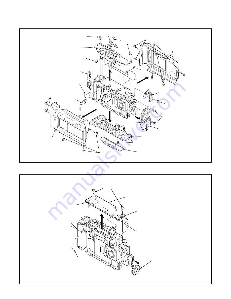
2-1. REMOVAL OF CABINET ASSEMBLY (FRONT) AND CABINET ASSEMBLY (BACK)

2-2. REMOVAL OF SY1 BOARD

20. Two screws 1.7 x  2.5

21. Holder card

17. Slide the
      cover jack.

18. Two screws
      1.7 x 3.0

14. Screw
      1.7 x 2.5

15. Dec cabinet R

16. Holder
      bracket R

6. Cover card

1. Three screws
    1.7 x 3.0

3. Three screws
    1.7 x 3.0

5. Cabinet
     front

4. Connector

22. Dec cabinet L

12. Screw 1.7 x 2.5

11. Spacer holder F2

9. Screw 1.7 x 2.5

10. Cabinet top

8. Button info

13. FPC

12. Screw
      1.7 x 2.5

2. Cabinet
    back

1. Five screws
    1.7 x 3.0

7. Screw
    1.7 x 4.0

19. Holder
      terminal

1. Two screws 1.7 x 2.5

2. Connector

3. Remove the solders.

4. Connector

5. SY1 board

6. speaker

7. Heat sink rubber A

8. Heat sink A

Summary of Contents for VPC-SX500

Page 1: ... are of special significance to product safety Should any component designated by a symbol need to be replaced use only the part designated in the Parts List Do not deviate from the resistance wattage and voltage ratings shown CAUTION Danger of explosion if battery is incorrectly replaced Replace only with the same or equivalent type recommended by the manufacturer Discard used batteries according...

Page 2: ...CIRCUIT DESCRIPTION Around CCD block 1 IC Configuration IC903 ICX245 CCD imager IC902 74ACT04MTC H driver IC907 CXD3400N V driver IC905 AD9803 CDS AGC A D converter 2 IC903 CCD Structure Interline type CCD image sensor Optical size 1 2 inch format Effective pixels 1392 H 1040 V Pixels in total 1434 H 1050 V Actual pixels 1360 H 1024 V Optical black Horizontal H direction Front 2 pixels Rear 40 pix...

Page 3: ...C102 is the reset gate clock 4 IC905 CDS AGC Circuit and A D Converter The video signal which is output from the CCD is input to Pins 26 and 27 of IC905 There are S H blocks inside IC905 generated from the XSHP and XSHD pulses and it is here that CDS correlated double sampling is carried out After passing through the CDS circuit the signal passes through the AGC amplifier It is A C converted inter...

Page 4: ...mes deep Thus the potential of the floating diffusion changes in proportion to the quantity of transferred electric charge and becomes CCD output after being received by the source follower The equivalent circuit for the output circuit is shown in Fig 1 7 H1 H2 H1 H2 H1 HOG RG CCD OUT PD Floating diffusion 1 H1 H2 H1 H2 H1 HOG RG CCD OUT PD 2 H1 H2 H1 H2 H1 HOG RG CCD OUT 3 H1 H2 RG CCD OUT 3 5V 0...

Page 5: ... digital signals 1 8 8 bit A D circuit Audio The audio signals which were converted to digial form by the 8 bit A D circuit are temporarily to a sound buffer and then recorded in the SSFDC card During playback the 8 bit D A circuit converts these signals into analog audio signals 1 9 Sound buffer Audio memory 1 10 LCD driver The Y C signals which are input to the LCD driver are con verted to RGB s...

Page 6: ...y as for EE the data is then sent to the SDRAM after which D A conversion is carried out inside the ASIC and then the data is sent to the LCD panel and displayed The LCD driver is converted Y C signals to RGB signals from ASIC and these RGB signals and the control signal which is output by the LCD driver are used to drive the LCD panel The RGB signals are 1H transposed so that no DC compo nent is ...

Page 7: ... is necessary for controlling the power supply for a PWM type switching regulator and is pro vided with one built in channel Feedback from 15 mA L power supply output is received and the PWM duty is varied so that each one is maintained at the correct current setting level 3 1 Protection circuit If output is short circuited for the length of time determined by the condenser which is connected to P...

Page 8: ...ed at the correct voltage set ting level 2 1 Short circuit protection circuit If output is short circuited for the length of time determined by the condenser which is connected to Pin 17 of IC501 all output is turned off The control signal P ON P A ON and LCD ON are recontrolled to restore output 3 Digital 3 3 V Power Output 3 3 V D is output Feedback for the 3 3 V D is provided to the switching c...

Page 9: ... current which is generated at the secondary side of T5401 is rectified to produce a high voltage direct current and is accumulated at electrolytic ca pacitor C5412 on the main circuit board 1 6 Voltage monitoring circuit This circuit is used to maintain the voltage accumulated at C5412 at a constance level After the charging voltage is divided and converted to a lower voltage by R5417 and R5419 i...

Page 10: ...ta input ASIC Serial communication data output ASIC Serial communication clock output ASIC Connect to GND Main clock oscillation terminal Main clock oscillation terminal 4 MHz VDD Sub clock oscillation terminal Sub clock oscillation terminal 32 768 kHz Reset input Battery OFF detection signal L OFF RS 232C RXD input terminal Serial communication request signal L Request Key matrix output 1 6 SY1 C...

Page 11: ...ts The 8 bit microprocessor reads the signals from each sensor element as input data and outputs this data to the camera circuits ASIC or to the LCD display device as operation mode setting data Fig 4 1 shows the internal commu nication between the 8 bit microprocessor and ASIC 3 Key Operaiton For details of the key operation refer to the instruction manual 8 bit microprocessor ASIC S REQ ASIC TES...

Page 12: ...is carried out even when the power switch is turned off so that the camera can start up again When the battery is removed the 8 bit micro processor operates in sleep mode using the backup capacitor At this time the 8 bit microprocessor only carries out clock counting and waits in standby for the battery to be attached again When a switch is operated the 8 bit microprocessor supplies power to the s...

Page 13: ...older bracket R 6 Cover card 1 Three screws 1 7 x 3 0 3 Three screws 1 7 x 3 0 5 Cabinet front 4 Connector 22 Dec cabinet L 12 Screw 1 7 x 2 5 11 Spacer holder F2 9 Screw 1 7 x 2 5 10 Cabinet top 8 Button info 13 FPC 12 Screw 1 7 x 2 5 2 Cabinet back 1 Five screws 1 7 x 3 0 7 Screw 1 7 x 4 0 19 Holder terminal 1 Two screws 1 7 x 2 5 2 Connector 3 Remove the solders 4 Connector 5 SY1 board 6 speake...

Page 14: ...1 7 x 2 5 2 Two screws 1 7 x 3 0 2 Two screws 1 7 x 3 0 3 Remove the solders 4 Holder battery 5 Three screws 1 7 x 2 5 6 PW1 board 7 Holder chassis F 1 Two screws 1 7 x 3 5 5 Holder chassis B 3 FPC 4 LCD 2 Connector 12 Three screws 1 7 x 2 5 10 Connector 6 FPC 11 CA1 board 9 FPC 7 Two screws 2 0 x 6 0 8 Screw 2 0 x 2 5 ...

Page 15: ...A2 BOARD 2 6 BOARD LOCATION CA1 board SY1 board PW1 board CA2 board CA3 board 1 Three screws 1 7 x 2 5 7 CA2 board 8 Holder chassis M 2 Two screws 1 7 x 4 0 3 Lens VF 4 Two screws 1 7 x 2 5 5 Two connectors 4 Screw 1 7 x 2 5 6 CA3 board ...

Page 16: ... than these should be carried out in sequence For 12 carry out adjustment after sufficient charging has taken place 3 4 Setup 1 System requirements Windows 95 or 98 IBM R compatible PC with 486 or higher processor CD ROM drive 3 5 inch high density diskette drive Serial port with standard RS 232C interface 8 MB RAM Hard disk drive with at least 15 MB available VGA or SVGA monitor with at least 256...

Page 17: ...over on the side of the camera Press on the arrows and slide the cover down to open it 3 Line up the arrow on the cable connector with the notch on the camera s serial port Insert the connector 4 Line up the serial connector on the cable with one of the serial ports on your computer and insert the connector 5 Turn on the camera and your computer system ...

Page 18: ...1 Voltage adjustment is necessary to repair in the CA3 board and replace the parts 2 Power voltage set about 3 0 V 3 After adjustment re connect the flexible cable of the LCD panel and CN171 as they were before Preparation 1 Remove the sub chassis to which the LCD panel is attached CN512 which is used for backlighting should always be left still connected 2 Open the barrier switch Measuring Point ...

Page 19: ...ght illumination with no flicker Illumination above the subject should be 400 lux 10 Adjustment method 1 Set the siemens star chart 95 cm 3 cm so that it be comes center of the screen 2 Double click on the DscCalV122 3 Click the Focus and click the Yes 4 Lens adjustment value will appear on the screen 5 Click the OK 12 CCD Defect Detect Adjustment Adjustment method 1 Double click on the DscCalV122...

Page 20: ... 0 3 Vp p 13 3 LCD Gain Adjustment Adjusting method 1 Adjust LCD Gain so that the amplitude of the CL173 wave form is 4 0 V 0 1 Vp p Note 13 2 LCD RGB Offset adjustment should always be carried out first 7 3 V 0 3 Vp p CL173 waveform 13 4 LCD Blue Brightness Adjustment Adjusting method 1 Adjust LCD B Bright so that the amplitude of the CL171 waveform is VG 0 2 0 05 Vp p with respect to the CL173 V...

Page 21: ... should always be carried out last Waveform CL173 Waveform CL172 VG 0 1 0 05 Vp p VG 13 5 LCD Red Brightness Adjustment Adjusting method 1 Adjust LCD R Bright so that the amplitude of the CL172 waveform is VG 0 1 0 05 Vp p with respect to the CL173 VG waveform Note 13 2 LCD RGB Offset adjustment and 13 3 LCD Gain ad justment should always be carried out first ...

Page 22: ...CHECK IC111 9 L1106 SD CLK 57 MHz OSCILLATION IC106 107 38 SD RAM IC106 IC107 MOVEMENT CLOCK NO READ PROGRAM FROM IC121 IF ABSENT CHECK IC102 IC106 IC107 IC102 140 141 IC301 75 76 CHECK SOLDERING OF EACH ASIC AND MEMORY PIN INCORRECT HANDSHAKING BETWEEN 8 BIT CPU AND RS 232C CHECK EACH INTERFACE PUSH SUTTER BUTTON IC301 2 3 SCAN IN 4 5 PULSE INPUT CHECK R3025 R3026 D3067 D3068 CN301 7 8 P ON P A O...

Page 23: ...05 LABEL COVER CARD SX112 J 22 411 018 1802 SCR PAN PCS 1 7X2 5 23 411 177 8407 SCR S TPG PAN PCS 1 7X3 24 636 054 7216 SPRING P COVER SX112 J 25 636 055 2418 COMPL COVER BATT SX112 J 26 Do not use 27 636 056 4947 SPACER HOLDER F2 SX112 J 28 636 056 2523 HEAT SINK RUBBER A SX112J 29 636 054 7186 SHAFT STRAP SX112 J 30 636 054 6929 DEC CABINET L SX112 J 31 636 054 6851 COVER JACK SX112 J 32 636 054...

Page 24: ...NLY 23 636 055 4931 COMPL PWB CA 3 VPC SX500EX ONLY 24 636 056 2653 SPACER LENS SX112 J 25 411 018 3707 SCR PAN PCS 1 7X4 26 636 054 7155 REFLECTOR POWER SX112 J 27 636 056 2646 SPACER CHASSIS M SX112 J 28 636 054 7025 HOLDER CHASSIS M SX112 J 29 636 049 6026 SPRING BATTERY SR6 J 30 636 054 6974 HOLDER SP HOOK SX112 J 31 636 054 7117 HOLDER BATTERY R SX112 J 32 636 055 4658 LABEL CAUTION BATT SX11...

Page 25: ...0V C9121 403 296 1308 TA SOLID 10U M 20V C9122 403 322 1005 CERAMIC 0 1U Z 16V C9123 403 322 1005 CERAMIC 0 1U Z 16V C9124 403 283 6309 CERAMIC 1U Z 10V C9125 403 283 6309 CERAMIC 1U Z 10V C9126 403 283 6309 CERAMIC 1U Z 10V C9127 403 276 1007 CERAMIC 0 01U K 16V C9129 403 276 1007 CERAMIC 0 01U K 16V C9130 403 322 1005 CERAMIC 0 1U Z 16V C9132 403 283 6309 CERAMIC 1U Z 10V C9133 403 276 1007 CERA...

Page 26: ...5 020 1899 INDUCTOR 68 OHM L1501 645 021 1737 INDUCTOR 47U J L1502 645 035 7190 INDUCTOR 33U J CAPACITORS C1005 403 343 8700 CERAMIC 1U M 12V C1007 403 343 8700 CERAMIC 1U M 12V C1008 403 323 6306 CERAMIC 0 1U K 16V C1011 403 323 6306 CERAMIC 0 1U K 16V C1012 403 323 6306 CERAMIC 0 1U K 16V C1014 403 283 6309 CERAMIC 1U Z 10V C1031 403 322 1005 CERAMIC 0 1U Z 16V C1034 403 322 1005 CERAMIC 0 1U Z ...

Page 27: ...03 MT GLAZE 0 000 ZA 1 16W R1530 401 226 2401 MT GLAZE 560 JA 1 16W R1531 401 226 2401 MT GLAZE 560 JA 1 16W R1533 401 226 1503 MT GLAZE 0 000 ZA 1 16W R1534 401 224 8900 MT GLAZE 100K JA 1 16W R1602 401 226 1503 MT GLAZE 0 000 ZA 1 16W R1603 401 226 1503 MT GLAZE 0 000 ZA 1 16W R1604 401 225 1207 MT GLAZE 4 7K JA 1 16W R1605 401 225 1207 MT GLAZE 4 7K JA 1 16W R1607 401 224 9303 MT GLAZE 1K JA 1 ...

Page 28: ...1 166 8303 MT FILM 1 2K DU 1 16W R5101 401 105 7909 MT GLAZE 0 000 ZA 1 16W R5102 401 166 9300 MT FILM 3 9K DU 1 16W R5103 401 105 0702 MT GLAZE 100K JA 1 16W R5104 401 105 5400 MT GLAZE 47K JA 1 16W R5105 401 166 3308 MT FILM 10 DC 1 16W R5106 401 166 3308 MT FILM 10 DC 1 16W R5107 401 166 4305 MT FILM 27 DC 1 16W R5108 401 166 4305 MT FILM 27 DC 1 16W R5200 401 037 5004 MT GLAZE 0 000 ZA 1 10W R...

Page 29: ...03 345 3000 POS SOLID 47U M 6 3V C5073 403 345 3000 POS SOLID 47U M 6 3V C5401 403 345 3000 POS SOLID 47U M 6 3V C5403 403 338 2904 CERAMIC 0 47U K 10V C5404 403 276 1304 CERAMIC 1000P K 50V C5406 403 343 3101 CERAMIC 1U K 6 3V C5407 403 276 1007 CERAMIC 0 01U K 16V C5409 403 284 7701 CERAMIC 0 033U Z 16V C5410 403 341 4407 CERAMIC 0 047U K 350V C5411 403 330 5903 CERAMIC 0 01U K 500V C5412 404 07...

Page 30: ...6 8EU IC302 409 383 1008 S 8423NFS IC303 410 298 3605 IC S 8324A50MC EPE IC311 409 407 0505 IC TK11331BM IC312 409 432 2505 IC LMV321M7X IC313 409 432 2505 IC LMV321M7X IC314 409 446 7305 IC TPA301D SOL008 P 0150 IC315 409 432 2505 IC LMV321M7X DIODES D3024 407 162 8507 DIODE DAN222 D3041 407 199 1809 LED SML 020MLT VF LED D3042 407 187 6304 LED SML 110VT SELF TIMER LED D3051 407 149 0807 DIODE 1S...

Page 31: ...E 100K JA 1 16W R3153 401 105 0603 MT GLAZE 10K JA 1 16W R3154 401 113 6208 MT GLAZE 3 6K JA 1 16W R3155 401 105 1105 MT GLAZE 12K JA 1 16W R3157 401 105 5400 MT GLAZE 47K JA 1 16W R3161 401 105 4809 MT GLAZE 390K JA 1 16W R3162 401 105 5400 MT GLAZE 47K JA 1 16W R3163 401 105 7909 MT GLAZE 0 000 ZA 1 16W R3164 401 113 6703 MT GLAZE 9 1K JA 1 16W R3166 401 105 0504 MT GLAZE 1K JA 1 16W R3167 401 1...

Page 32: ...OVERALL WIRING ...

Page 33: ...Nov 99 4 760 MI Printed in Japan SANYO Electric Co Ltd Osaka Japan ...

Reviews: