SATELLINE-M3-TR3,
–
TR4 and -R4
Integration Guide, Version 3.0
12
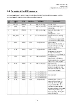
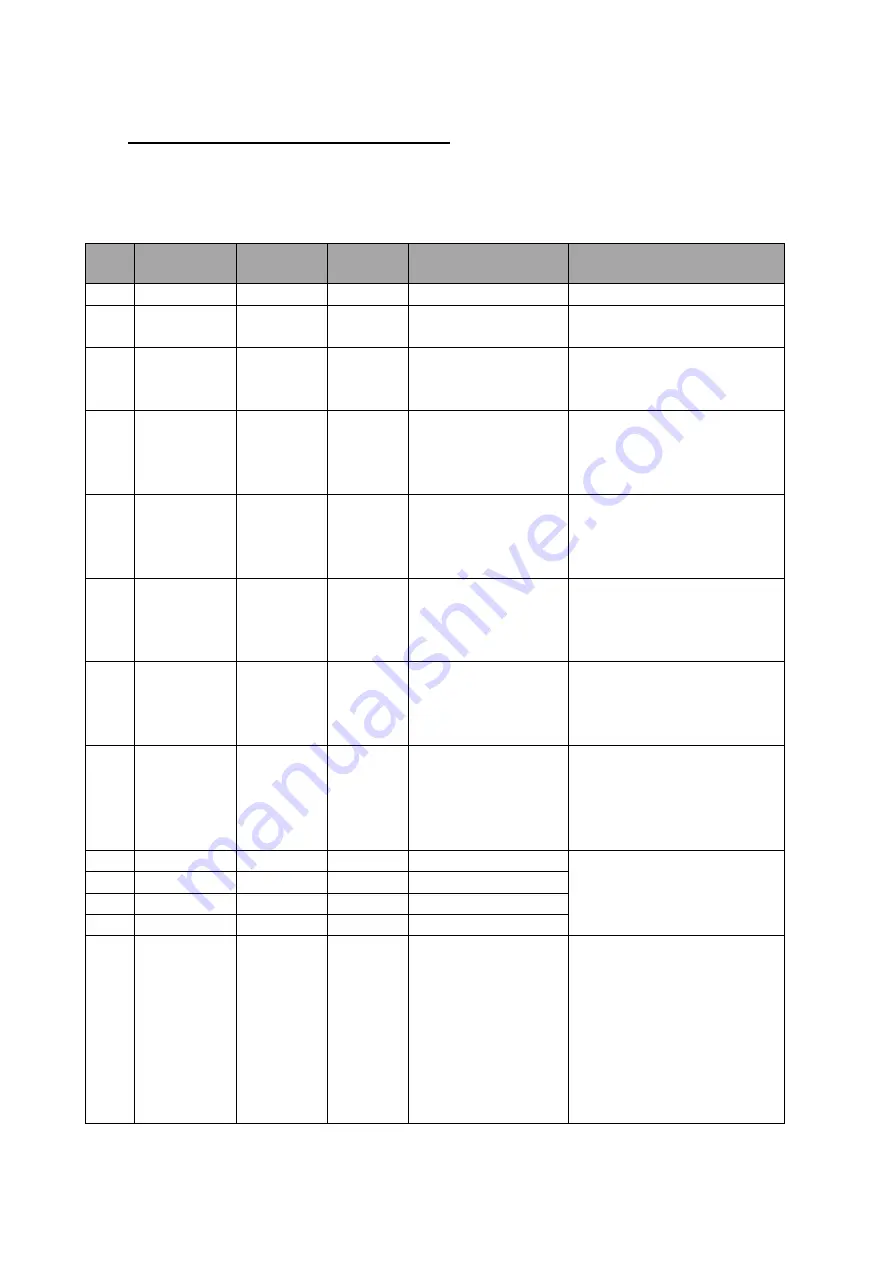
1.4
Pin order of the DTE connector
Direction
IN
is data from DTE (Data Terminal Equipment) to the radio transceiver module.
Direction
OUT
is data from the radio module to the DTE.
Pin
No.
Signal
name
Type
Direction
Pin State
Description
1,2
VCC_IN
POWER
IN
External Voltage
4.0V DC input
3,4
GND
GND
-
External Ground
Ground reference for power
and signals
5
VCC_IO
POWER
IN
External Voltage
Device IO driver input DC
voltage.
Voltage= 1.8 … 3.3
V
6
ENA_MOD
IO
IN
Internal Pull Down
Enable module by pulling
HIGH.
>1.2 V= Module power is ON,
<0.2 V= Module power is OFF
7
RD1
CMOS
OUT
Output Driver
Receive data.
Data received by module is
output on this pin. Driving
this pin is prohibited.
8
CTS1
CMOS
OUT
Output Driver
Clear To Send.
Module signals when it is
ready to receive data.
Driving this pin is prohibited.
9
TD1
CMOS
IN
Internal Pull Up
Transmit Data.
Data from DTE to module
shall be sent on this pin. Pull
LOW or drive LOW or HIGH.
10
RTS1
CMOS
IN
Internal Pull Up
Ready to send.
DTE can use this pin to signal
when it is ready to receive
data from module. Pull LOW
or drive LOW or HIGH.
11
GPIO1
CMOS
IN
Internal Pull Down
Unconnected.
12
GPIO2
CMOS
IN
Internal Pull Down
13
GPIO3
CMOS
IN
Internal Pull Down
14
GPIO4
CMOS
IN
Internal Pull Down
15
STAT
CMOS
OUT
Output Driver
Status signal. “1” when
device is OK and working
normally. Various toggle
sequences for other state
indications. See separate
section of manual. Can drive
LED directly. 10mA output
drive capability. Driving this
pin is prohibited.


