CQ7-A30
CQ7-A30 - Rev. First Edition: 1.0 - Last Edition: 2.0 - Author: S.B. - Reviewed by G.G. Copyright © 2016 SECO S.r.l.
23
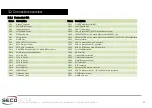
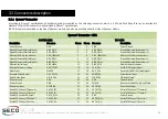
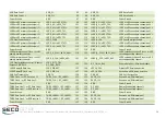
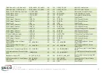
3.2.2
Jumpers list
Name Description
Name Description
JP1
PCI-e lanes routing selection
JP16
FAN #1 voltage selection
JP4
Boot source selection
JP17
FAN #1 PWM control enable
JP5
GP_1-Wire Bus mode selector
JP18
MFG_NC3 Pull-up or pull-down
JP6
miniPCI-e Wireless operations enable
JP19
MFG_NC4 Pull-up or pull-down
JP10
CAN voltage selector
JP20
MFG_NC2 routing to MFG or Debug USB connector
JP11
120
Ω
CAN termination
JP21
MFG_NC1 routing to MFG or Debug USB connector
JP12
POST Codes address selector
JP23
AT/ATX mode selection
JP13
Battery/batteryless selection
JP24
SRST# source selection
JP14
LIDBTN#
JP25
MFG_NC4 connection on CN41 pin #3
JP15
FAN #0 voltage selection
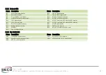
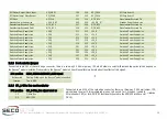
3.2.3
Dip Switch list
Name Description
Name Description
SW1
I2C EEPROM Address select
SW11
GP_PWM / GP_Timer selector
SW2
SuperIOs enable and address select
SW12
XR28V384 COM #2 / #3 mode selector
SW6
USB 3.0 / 2.0 ports selector


