background image


CQ7-A30


CQ7-A30 - Rev. First Edition: 1.0 - Last Edition: 2.0 - Author: S.B. - Reviewed by G.G. Copyright © 2016 SECO S.r.l.  

64 

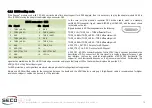
SRST# signal (pin 15 of connector CN41) can have two different routings, depending on the settings of 
jumper JP24 


Two other 3-way jumpers can be used to place a pull-up or pull-down resistor on signals MFG_NC3 and 
MFG_NC4. 


When  MFG_NC1  and  MFG_NC2  signals  are  not  routed  to  connector  CN41  (i.e.,  jumpers  JP20  and  JP21  are  set  to  position  2-3),  then  it  is 
possible to have a debug USB port on mini-B USB connector CN42 

This debug USB port is realised converting the Debug UART signals to USB by using a Silicon Labs

®

 CP2104 USB-to-UART bridge. 

By using Silicon Labs

®

 VCP drivers on the PC connected to this USB port (drivers available at 

http://www.silabs.com/products/interface/usbtouart/Pages/usb-to-

uart-bridge.aspx)

, the debug USB port will be exploitable by any COM port application, exactly like if it were a standard serial port. Please remember that Qseven

®


module will have to work in device (i.e. client) mode. 

JP24 position  SRST# connected to  

1-2 

RSTBTN# signal 

2-3 

MFG_NC4 signal 

JP18 position  MFG_NC3 pull-up / pull-down 

1-2 

10k

Ω

 pull-up to +3.3V_S 

2-3 

10k

Ω

 pull-down 


JP19 position


MFG_NC4 pull-up / pull-down


1-2 

10k

Ω

 pull-up to +3.3V_S 

2-3 

10k

Ω

 pull-down 

Summary of Contents for Qseven CQ7-A30

Page 1: ...CQ7 A30 Cross Platform Carrier Board for Qseven Rel 2 0 Compliant modules...

Page 2: ...curacy of this manual However SECO S r l accepts no responsibility for any inaccuracies errors or omissions herein SECO S r l reserves the right to change precise specifications without prior notice t...

Page 3: ...IEW 13 Chapter 2 2 1 Introduction 14 2 2 Technical Specifications 15 2 3 Electrical Specifications 16 2 3 1 RTC Battery 16 2 3 2 Power Rails meanings 17 2 3 3 Power LEDs 17 2 4 Mechanical Specificatio...

Page 4: ...CAN Interface 56 3 3 17 PS 2 Mouse Keyboard Pin header 57 3 3 18 LPC GPIO Pin header 57 3 3 19 POST Codes section 58 3 3 20 SPI Pin header 59 3 3 21 SPI Flash socket 59 3 3 22 I2C EEPROM socket 60 3 3...

Page 5: ...Last Edition 2 0 Author S B Reviewed by G G Copyright 2016 SECO S r l 5 Chapter 1 Warranty Information and assistance RMA number request Safety Electrostatic Discharges RoHS compliance Terminology and...

Page 6: ...RMA authorisation number must be put both on the packaging and on the documents shipped with the items which must include all the accessories in their original packaging with no signs of damage to or...

Page 7: ...ssible to send the faulty product to the SECO Repair Centre In this case follow this procedure o Returned items must be accompanied by a RMA Number Items sent without the RMA number will be not accept...

Page 8: ...voltages caused by static electricity could damage some or all the devices and or components on board 1 6 RoHS compliance The CQ7 A30 board is designed using RoHS compliant components and is manufactu...

Page 9: ...tal Visual interface a type of digital video display interface eDP embedded Display Port a type of digital video display interface developed especially for internal connections between boards and digi...

Page 10: ...different Input Output devices like cameras GPS Tuners and so on SIM Subscriber Identity Module a card which stores all data of the owner necessary to allow him accessing to mobile communication netw...

Page 11: ...definition audio specification pdf HDMI http www hdmi org index aspx I2C http www nxp com documents other UM10204_v5 pdf I2S https www sparkfun com datasheets BreakoutBoards I2SBUS pdf LPC Bus http ww...

Page 12: ...ion 2 0 Author S B Reviewed by G G Copyright 2016 SECO S r l 12 TMDS http www siliconimage com technologies tmds USB 2 0 and USB OTG http www usb org developers docs usb_20_070113 zip USB 3 0 http www...

Page 13: ...A30 Rev First Edition 1 0 Last Edition 2 0 Author S B Reviewed by G G Copyright 2016 SECO S r l 13 Chapter 2 Introduction Technical Specifications Electrical Specifications Mechanical Specifications B...

Page 14: ...oard can take advantage of all possible features that can be offered by x86 and or ARM architectures on Qseven modules The list of features that can effectively be used depends on the Qseven module us...

Page 15: ...connectors In Out Audio Expansion Slot Serial Ports CAN Bus both at TTL interface on internal pin header and with CAN transceiver on DB9 connector 3 x RS 232 only ports 2 x RS 232 RS 422 RS 485 confi...

Page 16: ...even module and of all the external devices and or the adapter boards connected to the system which take their power supply directly from the carrier board This way it will be possible to choose a PSU...

Page 17: ...3V_A _U unswitched ACPI S3 voltages i e power rails that are active both in ACPI s S0 Working and S3 Standby state Examples 1 5V_U 5V_SB_Q7 Qseven Module Standby voltage This power rail is used exclu...

Page 18: ...r disturbance rejection In order to fix the Qseven module to the carrier board on CQ7 A30 are soldered four metallic spacers height 5mm 2 5mm diameter that can be used for the fixing of standard size...

Page 19: ...header HDMI DP Slot SPI Pin Header SPI Flash Socket I2C EEPROM Socket FAN connectors Feature Pin header 2 x RS 232 422 485 Transceiver Coin Cell battery holder Power Section Power connectors Audio PC...

Page 20: ...CQ7 A30 CQ7 A30 Rev First Edition 1 0 Last Edition 2 0 Author S B Reviewed by G G Copyright 2016 SECO S r l 20 Chapter 3 Connectors placement Connectors overview Connectors description...

Page 21: ...DHG COM Ports Ethernet connector SPI pin header miniSIM Card slot I2C EEPROM Socket Feature pin header SPI Flash Socket PS 2 mouse and keyboard header FAN connectors SATA Power Mini Fit Power connecto...

Page 22: ...nnector CN9 SATA 1 F 7 15p connector CN31 USB 3 0 Host port 0 Type A receptacle CN10 SATA Power connector CN32 USB 2 0 Host ports 6 7 pin header CN11 SATA 0 M 7p connector CN33 USB 3 0 OTG port 1 micr...

Page 23: ...C4 Pull up or pull down JP10 CAN voltage selector JP20 MFG_NC2 routing to MFG or Debug USB connector JP11 120 CAN termination JP21 MFG_NC1 routing to MFG or Debug USB connector JP12 POST Codes address...

Page 24: ...b s link indicator Gigabit Ethernet differential pair 1 GBE_MDI1 9 10 GBE_MDI0 Gigabit Ethernet differential pair 0 Gigabit Ethernet differential pair 1 GBE_MDI1 11 12 GBE_MDI0 Gigabit Ethernet differ...

Page 25: ...ial Data Input HDA_SDI I2S_SDI 65 66 GP0_I2C_CLK I2 C Bus Clock Line Audio Serial Data Output HDA_SDO I2S_SDO 67 68 GP0_I2C_DAT I2 C Bus Data Line Thermal Alarm Input THRM 69 70 WDTRIG Watchdog Trigge...

Page 26: ...8 GND Power Ground LVDS primary channel Clock or eDP primary auxiliary channel LVDS_A_CLK eDP0_AUX 119 120 LVDS_B_CLK eDP1_AUX LVDS secondary channel Clock or eDP secondary auxiliary channel LVDS prim...

Page 27: ...st To Send output PCI E Channel 1 Transmit PCIE1_TX 173 174 PCIE1_RX PCI E Channel 1 Receive PCI E Channel 0 Transmit PCIE1_TX 175 176 PCIE1_RX PCI E Channel 1 Receive TTL Serial Port Receive signal U...

Page 28: ...e 5V_S 221 222 5V_S Switched Power Supply Line Switched Power Supply Line 5V_S 223 224 5V_S Switched Power Supply Line Switched Power Supply Line 5V_S 225 226 5V_S Switched Power Supply Line Switched...

Page 29: ...000Mbps and with Fast Ethernet 10 100Mbps Networks It will configure automatically to work with the existing network Please be aware that it will work in Gigabit mode only in case that they are connec...

Page 30: ...rs CN49 and or CN32 The selection is made using dedicated Dip switch SW6 with the meaning shown in the table on the left Please be aware that switches 1 and 2 must be set accordingly to the functional...

Page 31: ...d cables whose SuperSpeed differential pairs are individually shielded inside the global cable s external shielding The USB 2 0 Host port 1 is always available on the connector CN33 only In case the Q...

Page 32: ...set to ON position When SW6 switch 1 is set to OFF position then USB 2 0 ports 6 and 7 coming out from the Qseven module will be available on an internal 9 pin standard male pin header CN32 p 2 54 mm...

Page 33: ...Q7 A30 carrier board are not directly carried tout to a specific DP or HDMI connector Instead they are directly routed to an internal slot PCI e x16 type so that it is possible to connect an additiona...

Page 34: ...D B25 A25 DP_AUX Display Port auxiliary channel Power Ground GND B26 A26 DP_AUX Display Port auxiliary channel TMDS Clock or DP Data Line 3 TMDS_CLK DP_LANE3 B27 A27 GND Power Ground TMDS Clock or DP...

Page 35: ...B56 A56 N C Not Connected Power Ground GND B57 A57 N C Not Connected Not Connected N C B58 A58 GND Power Ground Not Connected N C B59 A59 GND Power Ground Power Ground GND B60 A60 N C Not Connected P...

Page 36: ...rts eDP sharing the same pins This means that it is possible to have Qseven modules offering LVDS interface and other offering embedded Display Port interfaces For this reason these two interfaces on...

Page 37: ...B19 A19 N C Not Connected LVDS or eDP primary channel pair 1 LVDS_A1 eDP0_TX1 B20 A20 GND Power Ground Power Ground GND B21 A21 N C Not Connected Power Ground GND B22 A22 N C Not Connected LVDS or eDP...

Page 38: ..._CLK eDP1_AUX LVDS secondary channel Clock or eDP secondary auxiliary channel LVDS or eDP secondary channel pair 2 LVDS_B2 eDP1_TX2 B41 A41 GND Power Ground LVDS or eDP secondary channel pair 2 LVDS_B...

Page 39: ...A channel 0 is switched with mSATA Slot CN8 The switching is automatic depending on the presence or not of an mSATA device in the dedicated slot This means that if a mSATA disk is plugged in the slot...

Page 40: ...or Please notice that SATA connectors will work only in case the Qseven module carries out SATA Channel 1 on Qseven connector pins 30 32 36 38 In case the Qseven module used doesn t have these signals...

Page 41: ...o CN8 then CN11 will be disabled When a mSATA disk is plugged into the slot a red LED D2 will light Please be aware that mSATA slot will work only in case the Qseven module carries out SATA Channel 0...

Page 42: ...e pin out is the same of any standard SD or MMC 4 0 card For ESD protection on all signal lines are placed clamping diodes for voltage transient suppression Signals related to SDIO MMC cards are the f...

Page 43: ...nector type TE p n 103669 2 or equivalent for S PDIF Input connection Mating connector TE p n 487526 2 or equivalent with contacts TE series 487117 or 487406 Since the Qseven module can offer differen...

Page 44: ...AC 97 24MHz Serial Bit Clock or I2S Serial Data Clock signal General Purpose I2 C Bus Data line GP0_I2C_DAT B6 A6 AUDIO_SDO Audio Serial Data Output signal Power Ground GND B7 A7 AUDIO_SDIN Audio Ser...

Page 45: ...name Description 12V Power Rail 12V_S B1 A1 GND Hot Plug presence detect tied to GND 12V Power Rail 12V_S B2 A2 12V_S 12V Power Rail 12V Power Rail 12V_S B3 A3 12V_S 12V Power Rail Power Ground GND B...

Page 46: ...e lane 3 Receiver Not Connected RSVD B30 A30 PCIE3_RX PCI e lane 3 Receiver Hot Plug presence detect needed to enable clock PRSNT 2 B31 A31 GND Power Ground Power Ground GND B32 A32 RSVD Not connected...

Page 47: ...B60 A60 N C Not connected Power Ground GND B61 A61 N C Not connected Not Connected N C B62 A62 GND Power Ground Not Connected N C B63 A63 GND Power Ground Power Ground GND B64 A64 N C Not connected P...

Page 48: ...wer Rail 12V Power Rail 12V_S B3 A3 12V_S 12V Power Rail Power Ground GND B4 A4 GND Power Ground SM Bus Clock line SMB_CLK B5 A5 N C Not connected SM Bus Data line SMB_DAT B6 A6 N C Not connected Powe...

Page 49: ...1 GND Hot Plug presence detect tied to GND 12V Power Rail 12V_S B2 A2 12V_S 12V Power Rail 12V Power Rail 12V_S B3 A3 12V_S 12V Power Rail Power Ground GND B4 A4 GND Power Ground SM Bus Clock line SMB...

Page 50: ...C Not connected 3 3V Power Rail 3 3V_S B8 A8 N C Not connected Not connected N C B9 A9 3 3V_S 3 3V Power Rail 3 3V Auxiliary Power Rail 3 3V_A B10 A10 3 3V_S 3 3V Power Rail Wake signal for link react...

Page 51: ...s lane 0 Receiving Input Differential pair mPCIE_CLK mPCIE_CLK Reference Clock for miniPCI express slot Differential Pair PCIE_WAKE Board s Wake Input it must be externally driven by the miniPCI e mod...

Page 52: ...only clamping diodes for ESD protection on UIM signal and voltage lines Three SMT RED LEDs are present near this Mini PCI Express Card Slot to show the presence of an eventual Wi Fi PCI Express Card i...

Page 53: ...ed to the Serial Port managed directly by the Qseven module is the upper one the lower one is dedicated to the CAN port see par 3 3 16 Please remember that RS 232 signals RxD_0 TxD_0 RTS_0 and CTS_0 a...

Page 54: ...e 1 N C N C N C 10 N C N C N C 2 RxD_2 RX_2 N C 11 RxD_3 RX_3 N C 3 TxD_2 TX_2 RX_2 TX_2 12 TxD_3 TX_3 RX_3 TX_3 4 N C N C N C 13 N C N C N C 5 GND GND GND 14 GND GND GND 6 N C N C N C 15 N C N C N C...

Page 55: ...e table on the left Please remember that the serial ports offered by the LPC to UART bridge XR28V384 and or those offered by the LPC SuperI O W83627DHG will be available only in case that the Qseven m...

Page 56: ...ut directly from Qseven card edge connector The related signals are carried out an internal 10 pin standard male pin header CN32 p 2 54 mm 10 pin dual row h 6mm with the pinout shown in the table on t...

Page 57: ...GPIO Pin header The LPC bus used to manage the devices previously described in par 3 3 15 and 3 3 17 is also carried out on a dual row 14 pin P2 54mm standard pin header with the pinout shown in the t...

Page 58: ...ring It is shared with General Purpose I O 7 LPC_RST signal is derived by PLT_RST signal by buffering it using a CMOS buffer 3 3 19POST Codes section On x86 architectures during the boot phase usually...

Page 59: ...needed on the carrier board it is provided an 8 pin SOIC socket for the housing of SPI Flashes Socket is type LOTES p n ACA SPI 004 K0 or equivalent p 1 27mm with the pinout shown in the table on the...

Page 60: ...power down sequence The second pushbutton SW8 is placed on SLP_BTN signal Upon the pressure of this pushbutton the Qseven module will enter in a sleep state is such states are supported The third pus...

Page 61: ...table for a description of them A special consideration has to be made on signal GP_PWM_OUT 0 2 and GP_TIMER_IN These indeed are multiplexed signals available on Qseven card edge connector which can...

Page 62: ...This signal is derived directly from Qseven signal FAN_PWMOUT The second FAN Connector CN38 is a 3 pin single line TH connector type MOLEX 22 27 2031 or equivalent with pinout shown in the table on th...

Page 63: ...to the tables on the left When both JP20 and JP21 are set in position 1 2 then all MFG signals are available on the MFG connector CN41 which is a 2 54mm pitch connector type MOLEX p n 70246 2004 or e...

Page 64: ...is debug USB port is realised converting the Debug UART signals to USB by using a Silicon Labs CP2104 USB to UART bridge By using Silicon Labs VCP drivers on the PC connected to this USB port drivers...

Page 65: ...CQ7 A30 CQ7 A30 Rev First Edition 1 0 Last Edition 2 0 Author S B Reviewed by G G Copyright 2016 SECO S r l 65 Chapter 4 LVDS eDP Adapter Module VA64 DP HDMI Adapter Module VA65 Accessories Kit...

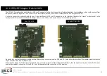
Page 66: ...aces LVDS or eDP depending on the interface offered by the Qseven module used in the Development Kit it is available an LVDS eDP Adapter module code VA64 which can be observed in the following picture...

Page 67: ...rimp terminals Display Data Channel signals are also provided in case that the Qseven module used supports them Most of the signals available on this connector come out directly from the Qseven connec...

Page 68: ...jumper JP2 which is a standard pin header P2 54mm 1x3 pin Similarly backlight software driven voltage signal LVDS_SW_BACK_FUSE can be regulated to be connected to 12VLVDS or 5VLVDS using module s jump...

Page 69: ...using module s jumper JP4 which is a standard pin header P2 54mm 1x3 pin Similarly backlight software driven voltage signal eDP_SW_BACK_FUSE can be regulated to be connected to 12VeDP or 5VeDP using...

Page 70: ...ACK_FUSE 5 eDP_SW_BACK_FUSE 6 N C 6 N C 7 N C 7 N C 8 LVDS_BLT_CTRL 8 LVDS_BLT_CTRL 9 eDP_BACKLIGHT_EN 9 eDP_BACKLIGHT_EN 10 GND 10 GND 11 GND 11 GND 12 GND 12 GND 13 GND 13 GND 14 eDP0_HPD 14 eDP1_HP...

Page 71: ...BACK_FUSE 3 eDP_SW_BACK_FUSE 3 eDP_SW_BACK_FUSE 4 eDP_SW_BACK_FUSE 4 eDP_SW_BACK_FUSE 5 eDP_SW_BACK_FUSE 5 eDP_SW_BACK_FUSE 6 N C 6 N C 7 N C 7 N C 8 LVDS_BLT_CTRL 8 LVDS_BLT_CTRL 9 eDP_BACKLIGHT_EN 9...

Page 72: ...by G G Copyright 2016 SECO S r l 72 29 eDP0_TX0 29 eDP0_TX0 30 GND 30 GND 31 eDP0_TX1 31 eDP0_TX1 32 eDP0_TX1 32 eDP0_TX1 33 GND 33 GND 34 eDP0_TX2 34 eDP0_TX2 35 eDP0_TX2 35 eDP0_TX2 36 GND 36 GND 3...

Page 73: ...I or DP depending on the interface offered by the Qseven module used in the Development Kit it is available a DP HDMI Adapter module code VA65 which can be observed in the following picture It is poss...

Page 74: ...description table for a correspondence between DP lanes and TMDS lanes DP_LANE0 DP_LANE0 Display Port differential pair 0 DP_LANE1 DP_LANE1 Display Port differential pair 1 DP_LANE2 DP_LANE2 Display P...

Page 75: ...HDMI_CEC HDMI Consumer Electronics Control CEC Line As already described in the description of DP connector CN4 this signal is in reality a General Purpose 1_wire bus interface that can be used for i...

Page 76: ...er for use in area Europe Indonesia Korea USA NEMA 5 15R to UK BS1363 Plug Adapter for use in area England Hong Kong U A E Singapore Malaysia 4 wire Power cable for the adapting of other external PSUs...

Page 77: ...A30 CQ7 A30 Rev First Edition 1 0 Last Edition 2 0 Author S B Reviewed by G G Copyright 2016 SECO S r l 77 SECO Srl Via Calamandrei 91 52100 Arezzo ITALY Ph 39 0575 26979 Fax 39 0575 350210 www seco...

Reviews: