CQ7-A30
CQ7-A30 - Rev. First Edition: 1.0 - Last Edition: 2.0 - Author: S.B. - Reviewed by G.G. Copyright © 2016 SECO S.r.l.
57
Please be aware that the support for legacy PS/2 peripherals is not provided for by Qseven
®
specifications. This means that the working of PS/2
interface depends strongly on the BIOS of the Qseven
®
module used, which might not manage this interface, even if it supports correctly the
W83627DHG SuperI/O. A customised BIOS could be necessary in order to enable PS/2 support.
3.3.17
PS/2 Mouse + Keyboard Pin header
On CQ7-A30 carrier board is also available a single row, 7-pin p2.54mm pin header, for the connection of legacy PS/2
peripherals (mouse and/or keyboard), managed by the LPC Super I/O W83627DHG (the same that manages
the serial ports available on combo connector CN12).
KEYB_DAT: PS/2 data line for keyboard connection
KEYB_CLK: PS/2 clock line for keyboard connection
MS_DAT: PS/2 data line for mouse connection
MS_CLK: PS/2 clock line for mouse connection
3.3.18
LPC/GPIO Pin header
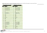
The LPC bus, used to manage the devices previously described in par. 3.3.15 and 3.3.17 is
also carried out on a dual row, 14 pin, P2.54mm standard pin header, with
the pinout shown in the table on the left.
Please remember that Qseven
®
specifications rel.2.0 share, on the same pins of the card
edge connector, the LPC signals with eight general Purpose I/Os; this means that whatever
interface is offered by the Qseven
®
module, it will be available on the pins of this pin header
connector.
Please refer to the User Manual of the Qseven
®
module used for a description of effective
signals available on this pin header, considering the correspondence with the card edge
connector.
LPC_AD[0..4]/GPIO[0..1] LPC command/address/data signals, General purpose I/O [0..3].
BUF_LPC_CLK: LPC Clock Output line. Since there are many devices on LPC bus on CQ7-
PS/2 Mouse + Keyboard
Pin header - CN13
Pin Signal
1
KEYB_DAT
2
N.C.
3
MS_DAT
4
GND
5
+5V
PS2
6
KEYB_CLK
7
MS_CLK
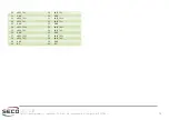
LPC/GPIO Pin Header - CN3
Pin Signal
Pin Signal
1
LPC_LDRQ#/GPIO7
2
LPC_AD0/GPIO0
3
N.C.
4
LPC_AD1/GPIO1
5
SERIRQ/GPIO6
6
LPC_AD2/GPIO2
7
LPC_FRAME#/GPIO5
8
LPC_AD3/GPIO3
9
LPC_RST#
10
GND
11
BUF_LPC_CLK
12
GND
13
+3.3V_S
14
+3.3V_S


