CQ7-A30
CQ7-A30 - Rev. First Edition: 1.0 - Last Edition: 2.0 - Author: S.B. - Reviewed by G.G. Copyright © 2016 SECO S.r.l.
63
3.3.26
Manufacturer and Debug Connectors
According to Qseven
®
specifications, on MXM connector there are some pins that are reserved for manufacturing and debugging purposes
(MFG_NC0÷MFG_NC4). These signals are reserved to the manufacturer of the Qseven CPU module, so it is not recommended to use them. Anyway they can be
accessed through two different connectors.
MFG_NCx signals can be used, by the Qseven
®
module, as a JTAG port or Debug UART. Please refer to the User manual of the Qseven
®
module for information
about the proper assignment of JTAG / UART signals to the MFG_NCx signals (although the assignment shall correspond to that defined by the Qseven
®
specifications).
Moreover, debug UART signals (available on MFG_NC1 and MFG_NC2 pins of Qseven
®
card edge
connector), can be routed to a standard connector or to an USB-to-UART bridge, which will allow the
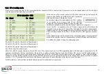
implementation of a debug USB port. Selection is made using jumpers JP20 and JP21, according to the
tables on the left.
When both JP20 and JP21 are set in position 1-2, then all MFG
signals are available on the MFG connector, CN41, which is a
2.54mm pitch connector, type MOLEX p/n 70246-2004 or
equivalent.
Mating connector: MOLEX 22-55-2202 receptacle with MOLEX
70058 or 71851 crimp terminals.
Please be aware that Debug UART, when routed to this connector (on pins dedicated to
signals MFG_NC1 and MFG_NC2) will be available at TTL level, i.e. it cannot be used for
a direct connection to a common RS-232 serial port (like those available on PCs).
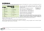
Regarding MFG_NC4 signal, a
dedicated 2-way jumper, JP25,
allows selecting if this signal must
be connected to pin #3 of CN41
or not (it could be routed to pin
15, see jumper JP24).
JP20 position MFG_NC2 routed to
1-2
JTAG connector CN41 (JTAG_TDI)
2-3
Debug USB port CN42 (DEBUG_RX)
JP21 position
MFG_NC1 routed to
1-2
JTAG connector CN41 (JTAG_TDO)
2-3
Debug USB port CN42 (DEBUG_TX)
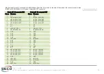
MFG connector - CN41
Pin Signal
Pin Signal
1
+3.3V_A
2
N.C.
3
MFG_NC4 (see JP25)
4
GND
5
MFG_NC2 (see JP20)
6
GND
7
MFG_NC3
8
GND
9
MFG_NC0
10
GND
11
10k
Ω
pull-down to GND
12
GND
13
MFG_NC1 (see JP21)
14
GND
15
SRST#
16
GND
17
N.C.
18
GND
19
N.C.
20
GND
JP25 position
MFG_NC4 connection on
CN41 pin #3
Not Inserted
Disconnected
Inserted
Connected


