background image


SBC-C20


SBC-C20 User Manual - Rev. First Edition: 1.0 - Last Edition: 1.0 - Author: A.R. - Reviewed by C.M. -Copyright © 2020 SECO S.p.A.  


35 


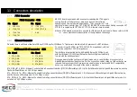
GPIO connector 

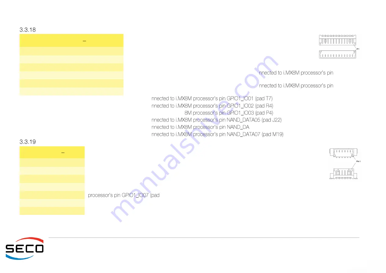
SECO SBC-C20 board offers a dedicated connector with 8x General Purpose GPIOs, 
directly managed by the i.MX8M processor. 

These GPIOS are available on connector CN38, which is a 10-pin p1.27mm connector 
type Molex p/n 53398-1071 or equivalent, with pinout shown in the table on the left. 

Mating connector: MOLEX 51021-1000 receptacle with 50079-8000 female crimp terminals. 
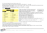
GPIO_0: General purpose IO #0, electrical level VDD_3P3V, co
ESCPI2_MOSI (pad E5) 
GPIO_1: General purpose IO #1, electrical level VDD_3P3V, co
ESCPI2_SCLK (pad C5) 

GPIO_2: General purpose IO #2, electrical level VDD_3P3V, co


GPIO_3: General purpose IO #3, electrical level VDD_3P3V, co


GPIO_4: General purpose IO #4, electrical level VDD_3P3V, connected to i.MX


GPIO_5: General purpose IO #5, electrical level VDD_3P3V, co


GPIO_6: General purpose IO #6, electrical level VDD_3P3V, co

TA06 (pad L19) 

GPIO_7: General purpose IO #7, electrical level VDD_3P3V, co


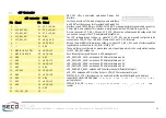
SPI Connector 

i.MX8M enhanced configurable serial peripheral interface (ECSPI) #1 is externally available on connector CN40, 
which is a 6-pin p1.27mm connector type Molex p/n 53398-0671 or equivalent, with pinout shown in the table 
on the left. 
Mating connector: MOLEX 51021-0600 receptacle with MOLEX 50079-8000 female crimp terminals. 
Signal description 
EXT_SPI_CS: SPI chip select, output signal, active high, electrical level VDD_3P3V. This signal is activated when 
this interface is used as communication with external devices. It is managed by i.MX8M signal ECSPI_SS02 through i.MX8M 

N6) 

EXT_SPI_MISO: SPI Master Input Slave Output, input signal, electrical level VDD_3P3V. 
EXT_SPI_MOSI: SPI Master Output Slave Input, ouput signal, electrical level VDD_3P3V. 
EXT_SPI_SCLK: SPI Serial Clock, electrical level VDD_3P3V 


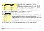
GPIO connector   CN38 

Pin   Signal 

Pin  Signal 

VDD_3P3V 

GPIO_4 

GPIO_0 

GPIO_5 

GPIO_1 

GPIO_6 

GPIO_2 

GPIO_7 

GPIO_3 

10 

GND 

SPI Connector   CN40 

Pin   Signal 

1


VDD_3P3V 

2


EXT_SPI_CS 

3


EXT_SPI_MISO 

4


EXT_SPI_MOSI 

EXT_SPI_SCLK 

GND 

Summary of Contents for SBC-C20

Page 1: ...SBC C20 Single Board Computer with NXP i MX 8M Applications Processors...

Page 2: ...has been made to ensure the accuracy of this manual However SECO S p A accepts no responsibility for any inaccuracies errors or omissions herein SECO S p A reserves the right to change precise specifi...

Page 3: ...d definitions 9 1 8 Reference specifications 11 OVERVIEW 12 2 1 Introduction 13 2 2 Technical specifications 14 2 3 Electrical specifications 15 RTC Battery 15 Power rails 15 2 4 Mechanical specificat...

Page 4: ...oSIM Card Slot 30 CSI Camera Connector 31 SD card slot 32 Audio connectors 33 Dual Analog Mic in Connector 34 Optional 10W Amplified Speaker Out Connector 34 Digital Mic In connector 34 GPIO connector...

Page 5: ...tion 1 0 Last Edition 1 0 Author S B A R Reviewed by C M Copyright 2020 SECO S p A 5 Warranty Information and assistance RMA number request Safety Electrostatic discharges RoHS compliance Terminology...

Page 6: ...line The RMA authorization number must be put both on the packaging and on the documents shipped with the items which must include all the accessories in their original packaging with no signs of dama...

Page 7: ...enter it is possible to send the faulty product to the SECO Repair Centre In this case follow this procedure o Returned items must be accompanied by an RMA Number Items sent without the RMA number wil...

Page 8: ...sing RoHS compliant components and is manufactured on a lead free production line It is therefore fully RoHS compliant Always switch the power off and unplug the power supply unit before handling the...

Page 9: ...for transferring data at very high speed using inexpensive twisted pairs copper cables usually used for video applications MAC Medium Access Controller the hardware implementing the Data Link Layer of...

Page 10: ...Bus System Management Bus a subset of the I2C bus dedicated to communication with devices for system management like a smart battery and other power supply related devices SPI Serial Peripheral Inter...

Page 11: ...w en analog interface lvds shtml http www ti com lit ug snla187 snla187 pdf M 2 Specifications https pcisig com specifications pciexpress M 2_Specification MMC eMMC https www jedec org committees jc 6...

Page 12: ...User Manual Rev First Edition 1 0 Last Edition 1 0 Author S B A R Reviewed by C M Copyright 2020 SECO S p A 12 Introduction Technical specifications Electrical specifications Mechanical specification...

Page 13: ...lot which allows plugging M 2 Modem modules with USB or PCI e interface and by an optional WiFi ac a b g n BT 5 0 combo embedded module The M 2 Key B Slot and the embedded modem can rely on an on boar...

Page 14: ...11 ac a b g n BT 5 0 module antenna on board M 2 Socket 2 Key B 2260 3042 Slot for WWAN modules microSIM slot soldered on board for the Modem USB Up to 2 x USB 2 0 Type A sockets Optional USB 2 0 inte...

Page 15: ...8mAh In case of exhaustion the battery should only be replaced with devices of the same type Always check the orientation before inserting and make sure that they are aligned correctly and are not dam...

Page 16: ...B A R Reviewed by C M Copyright 2020 SECO S p A 16 5V_ALW 5V Always voltage derived from VIN_SYS voltage VRTC 3V external voltage for supplying the RTC clock VDD_3P3V 3 3V switched voltage directly de...

Page 17: ...ition 1 0 Author S B A R Reviewed by C M Copyright 2020 SECO S p A 17 2 4 Mechanical specifications Board dimensions are 101 6 x 147 mm 4 x 5 78 The printed circuit of the board is made of ten layers...

Page 18: ...x Antenna WiFi 802 11a b g n BT LE module Power ON Connector Button USB2514 USB 2 0 Hub USB_2 Combo TRRS Internal audio connectors Speaker connector I2S Audio Codec Audio Amplifier MIPI_CSI GPIO I2C_2...

Page 19: ...SBC C20 SBC C20 User Manual Rev First Edition 1 0 Last Edition 1 0 Author A R Reviewed by C M Copyright 2020 SECO S p A 19 Introduction Connectors overview Connectors description...

Page 20: ...ease be aware that depending on the configuration purchased the appearance of the board can be significantly different from the following pictures microSIM Card Slot JTAG eDP USB Recovery LED Driver B...

Page 21: ...N17 I2C Touch Screen Connector CN35 Optional 10W Amplified Speaker Out Connector CN18 LVDS backlight connector CN37 Optional USB internal header CN19 HDMI connector CN38 GPIO Connector CN21 eDP connec...

Page 22: ...onfigure automatically to work with the existing network Please be aware that they will work in Gigabit mode only in case that they are connected to Gigabit Ethernet switches hubs routers For the conn...

Page 23: ...pin V_LED4 LED string 4 current input V_LED4 is the open drain output of an internal dimming control switch Connect the LED string 4 cathode to this pin I2C Touch Screen connector SBC C20 by iMX8M al...

Page 24: ...differential data pair 0 LVDS0_TX1 LVDS0_TX1 LVDS Channel 0 differential data pair 1 LVDS0_TX2 LVDS0_TX2 LVDS Channel 0 differential data pair 2 LVDS0_TX3 LVDS0_TX3 LVDS Channel 0 differential data p...

Page 25: ...2 001RLF Signals involved in HDMI management are the following TMDS_CLK TMDS_CLK TMDS differential Clock TMDS_LANE0 TMDS_LANE0 TMDS differential pair 0 TMDS_LANE1 TMDS_LANE1 TMDS differential pair 1 T...

Page 26: ...ese are factory configurations please take care of specifying which is the configuration needed for VCC_BKL_SW voltage rail Here following the signals involved in eDP management eDP_ML0P eDP_ML0N embe...

Page 27: ...ping diodes for voltage transient suppression The USB 2 0 port available on USB 3 0 connector can be switched to a standard micro AB connector described in the table on the left This connector must be...

Page 28: ...contro 5VUSB3 and 5VUSB4 voltages are derived from 5V_ALW power rail using a 500mA Dual Channel power switch Internal USB header As a factory option it is possible to provide SBC C20 board with an int...

Page 29: ...ir DIF1 _REF_CLK DIF1_REF_CLK PCI Express Reference Clock for lane 0 Differential Pair PCIE_RST Reset Signal that is sent from the i MX8M processor to the PCI e devices available on the module It is a...

Page 30: ...ng a dedicated jumper JP3 When JP3 is not placed this pin will be floating microSIM Card Slot Interfaced to the M 2 slot CN26 as already told in paragraph 3 3 10 there is a microSIM Card Slot to be us...

Page 31: ...N CSI Camera Clock input differential pair MIPI_CSI0_EN External camera module Power enable signal It is an active high signal with electrical level VDD_3P3V MIPI_CSI0_MCKL_OUT Master Clock it is mana...

Page 32: ...other one is used to manage a for the use of standard microSD cards which can be used as Mass Storage and or Boot Devices The connector is a microSD connector push push type H 2mm p n TKS0192003 SDIO_...

Page 33: ...Additionally it is available a dedicated output connector carrying out Headphone and Line Out stereo outputs For this purpose the connector used is CN32 which is a 8 pin p1 27mm connector type Molex...

Page 34: ...4Ohm load This connector is type MOLEX Micro Fit 3 0 p n 43045 0400 or equivalent AMP_SPEAKER_LP amplified line output Left channel AMP_SPEAKER_RP amplified line output Right channel Digital Mic In co...

Page 35: ...trical level VDD_3P3V co TA06 pad L19 GPIO_7 General purpose IO 7 electrical level VDD_3P3V co SPI Connector i MX8M enhanced configurable serial peripheral interface ECSPI 1 is externally available on...

Page 36: ...stor can be placed between CAN_H and CAN_L signals It can be connected or disconnected from the line by using JP4 jumper Jumper inserted termination connected Debug UART Connector Onboard connector CN...

Page 37: ...t to Send handshaking signal RS232_CTS COM PORT 4 RS 232 Clear To Send handshaking signal LCD Backlight Power Selection On SBC C20 board two dedicated PCB jumpers are available in order to select the...

Page 38: ...e on the left Mating connector MOLEX 51021 0200 crimp housing with MOLEX 50079 8000 crimp terminals Signals Description SYS_ONOFF Power switch input signal This signal has to be connected to an extern...

Page 39: ...SBC C20 SBC C20 User Manual Rev First Edition 1 0 Last Edition 1 0 Author A R Reviewed by C M Copyright 2020 SECO S p A 39 Thermal Design...

Page 40: ...reason a critical design parameter always to be kept in very high consideration is the thermal design and analysis of the final assembled system It is necessary to carefully consider the heat generate...

Page 41: ...BC C20 User Manual Rev First Edition 1 0 Last Edition 1 0 Author A R Reviewed by C M Copyright 2020 SECO S p A 41 SECO S p A Via A Grandi 20 52100 Arezzo ITALY Ph 39 0575 26979 Fax 39 0575 350210 www...

Reviews: