background image


SBC-C23


SBC-C23 User Manual - Rev. First Edition: 1.0 - Last Edition: 1.1 - Author: S.B. - Reviewed by L.B. -Copyright © 2020 SECO S.p.A.  

30 

3.3.13


Expansion connectors 

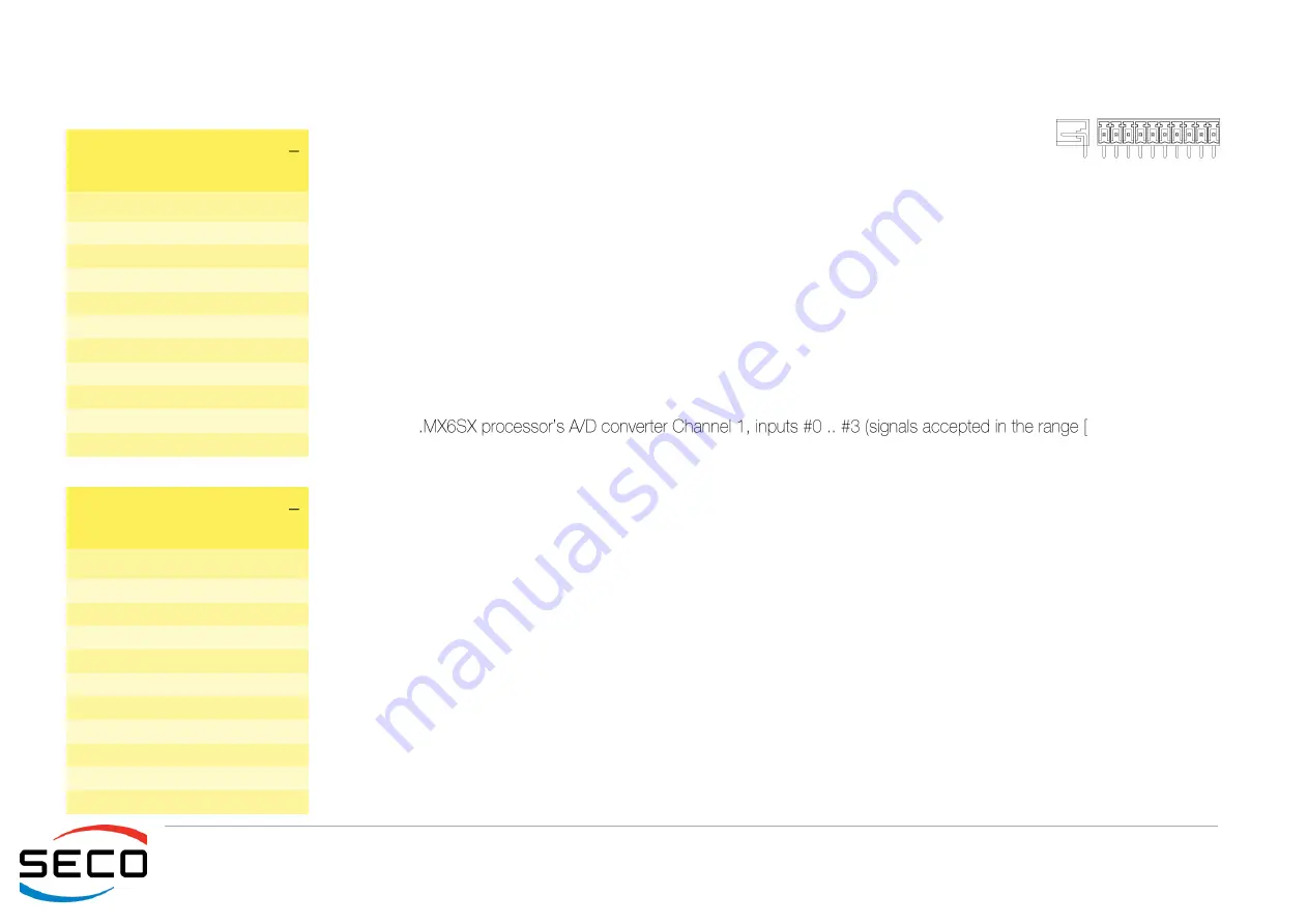
The  SBC-C23  board  offers  the  possibility  of  expanding  its  functionalities  by  using  some  additional 
interfaces,  available  on  two  dedicated  10-pin  PCB  terminal  blocks,  CN59  and  CN60,  type 
EUROCLAMP p/n PV08-3,81-H-P or equivalent.  

The pinout of these connectors are shown in the tables on the left .  

PWM_6_5V:  PWM  Output  signal,  electrical  level  VCC_SW  with  2k2

Ω

  pull-up  resistor.  It  is  managed  by  i.MX6SX  pin 

RGMII2_TD2. 

PWM_5_5V:  PWM  Output  signal,  electrical  level  VCC_SW  with  2k2

Ω

  pull-up  resistor.  It  is  managed  by  i.MX6SX  pin 

RGMII2_TD3. 

I2C2_SDA_5V: I2C Bus data line. Bidirectional signal, electrical level VCC_SW with a 2k2

Ω

 pull-up resistor. It is managed by 

i.MX6 processor

s I2C controller #2 (pin GPIO_3) 

I2C2_SCL_5V: I2C Bus clock line. Output signal, electrical level VCC_SW with a 2k2

Ω

 pull-up resistor. It is managed by i.MX6 

processor

s I2C controller #2 (pin GPIO_2) 

ADC_[0..3]: i

0..+3.3V]).  

RS_232_TX: i.MX6SX UART #2 transmit data signal, RS-232 electrical level. It is managed by i.MX6SX pin GPIO_IO06 

RS_232_RX: i.MX6SX UART #2 Receive data signal, RS-232 electrical level. It is managed by i.MX6SX pin GPIO_IO07 

RS_232_RTS: i.MX6SX UART #2 Request to Send signal, RS-232 electrical level. It is managed by i.MX6SX pin SD1_DATA3 

RS_232_CTS: i.MX6SX UART #2 Clear to Send signal, RS-232 electrical level. It is managed by i.MX6SX pin SD1_DATA2 

CAN ports: they are managed using as many  NXP TJA1051T High Speed CAN Transceivers. The i.MX6SX CAN port #1 is 
available on pins SD3_DATA7 and SD3_DATA5, while CAN port #2 is available on pins SD3_DATA6 and SD3_DATA4 

CAN1_H: High-Level CAN bus line, port #1. 

CAN1_L: Low-Level CAN bus line, port #1. 

CAN2_H: High-Level CAN bus line, port #2. 

CAN2_L: Low-Level CAN bus line, port #2. 

/RS485_D-:  :  RS-485  port,  differential  pair.  It  is  managed  using  i.MX6SX  UART  Port  #3,  available  on  pins 
QSPIB_SCLK, QSPIB_SS0_B and QSPIB_DATA0 (CTS signal, necessary to manage the direction of RS-485 port) 

VCC_OUT_5V: 5V switched voltage for I/Os, max 500mA, derived from VCC_SW voltage. 

Expansion Connector #1   

CN59 

Pin 

Signal 

VCC_OUT_5V 

GND_I/O 

PWM_6_5V 

PWM_5_5V 

I2C2_SDA_5V 

I2C2_SCL_5V 

ADC_0 

ADC_1 

ADC_2 

10 

ADC_3 

Expansion Connector #2   

CN60 

Pin 

Signal 

RS_232_TX 

RS_232_RX 

RS_232_RTS 

RS_232_CTS 

CAN1_H 

CAN1_L 

CAN2_H 

CAN2_L 


10 

RS485_D- 

Summary of Contents for SBC-C23

Page 1: ...Cn62 SBC C23 Single Board Computer with NXP i MX6SoloX Processor...

Page 2: ...S p A accepts no responsibility for any inaccuracies errors or omissions herein SECO S p A reserves the right to change precise specifications without prior notice to supply the best product possible...

Page 3: ...Introduction 13 2 2 Technical specifications 14 2 3 Electrical specifications 15 2 3 1 RTC Battery 15 2 3 2 Power rails 16 2 4 Mechanical specifications 17 2 5 Block diagram 18 CONNECTORS 19 3 1 Intr...

Page 4: ...ht 2020 SECO S p A 4 3 3 9 UART 5 Connector 28 3 3 10 Factory reset button connector 29 3 3 11 Boot Mode Selection jumper JP7 29 3 3 12 Boot Selection jumper JP8 29 3 3 13 Expansion connectors 30 3 3...

Page 5: ...dition 1 0 Last Edition 1 1 Author S B Reviewed by L B Copyright 2020 SECO S p A 5 Warranty Information and assistance RMA number request Safety Electrostatic discharges RoHS compliance Terminology an...

Page 6: ...ne The RMA authorization number must be put both on the packaging and on the documents shipped with the items which must include all the accessories in their original packaging with no signs of damage...

Page 7: ...ter it is possible to send the faulty product to the SECO Repair Centre In this case follow this procedure o Returned items must be accompanied by an RMA Number Items sent without the RMA number will...

Page 8: ...ng RoHS compliant components and is manufactured on a lead free production line It is therefore fully RoHS compliant Always switch the power off and unplug the power supply unit before handling the bo...

Page 9: ...nication systems Mbps Megabits per second MMC eMMC MultiMedia Card embedded MMC a type of memory card having the same interface of SD The eMMC are the embedded version of the MMC They are devices that...

Page 10: ...I Serial Peripheral Interface a 4 Wire synchronous full duplex serial interface which contemplates a master and one or more slaves individually enabled through a Chip Select line TBM To be measured TT...

Page 11: ...com ww en analog interface lvds shtml http www ti com lit ml snla187 snla187 pdf M 2 Specifications https pcisig com specifications pciexpress M 2_Specification MMC eMMC http www jedec org committees...

Page 12: ...23 User Manual Rev First Edition 1 0 Last Edition 1 1 Author S B Reviewed by L B Copyright 2020 SECO S p A 12 Introduction Technical specifications Electrical specifications Mechanical specifications...

Page 13: ...WWAN USB modules by an M 2 Key E Slot for the connection of modules with PCI e interface by an optional WiFi BT LE embedded module Single Band or Dual Band and by an optional modem soldered on board s...

Page 14: ...example Windows intends 1GB 1024 3 byte so global capacity shown for Disk Properties will be less than expected Please also consider that a portion of disk capacity will be used by internal Flash Cont...

Page 15: ...ime Clock embedded on the module which is a NXP PCF2123 If the board is not equipped with the optional rechargeable battery then it will be available a soldered horizontal 3V coin cell lithium battery...

Page 16: ...aning VIN 12VDC voltage directly coming from the Power Supply connectors CN1 or CN76 3V3_ALW 3 3V Always voltage derived from VCC_SW voltage VRTC 3V external voltage for supplying the RTC clock VCC_SW...

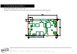
Page 17: ...dition 1 1 Author S B Reviewed by L B Copyright 2020 SECO S p A 17 2 4 Mechanical specifications Board dimensions are 89 5 x 153 mm 3 52 x 6 02 The printed circuit of the board is made of ten layers s...

Page 18: ...rocessor M 2 Key B Slot DDR3L System Memory Switch mode charger SD Card slot 2 x FastEthernet interface USB OTG 1 RGMII 1 2 LVDS I2C1 GPIO 3V Cabled Coin cell battery USB 2 0 Hub uSDHC3 UART6 SPI5 VRT...

Page 19: ...SBC C23 SBC C23 User Manual Rev First Edition 1 0 Last Edition 1 1 Author S B Reviewed by L B Copyright 2020 SECO S p A 19 Introduction Connectors overview Connectors description...

Page 20: ...hem on a panel of an eventual enclosure TOP SIDE BOTTOM SIDE Please be aware that depending on the configuration purchased the appearance of the board can be significantly different from the following...

Page 21: ...RT 5 CN3 LVDS CN70 Debug UART CN12 M 2 Key B Slot CN73 microSD Card Slot CN28 M 2 Key E Slot CN76 VIN Terminal block CN59 I O connector 1 CN79 Battery pack connector CN60 I O connector 2 J2 USB OTG mi...

Page 22: ...ferences Shielded cables are also recommended Here following the signals related to LVDS management LVDS0_TX0 LVDS0_TX0 LVDS Channel 0 differential data pair 0 LVDS0_TX1 LVDS0_TX1 LVDS Channel 0 diffe...

Page 23: ...OTG1_VBUS USB voltage rail It is an input for USB port working in Client mode an output for Host mode USB_ID Client Host identification signal This signal is high when the USB port works in client mod...

Page 24: ...e second port is a factory option 3 3 4 SD card slot The NXP i MX6 SoloX processor embeds four Ultra Secured Digital Host controllers uSDHC able to support SD SDIO MMC Cards For this reason on SBC C23...

Page 25: ...Managed through i MX6SX pin RGMII1_RD2 W_DISABLE M 2 module disable signal 100k pull up NVCC_1V8 active low output Managed through i MX6SX pin RGMII1_RD3 UIM_RST Reset signal line sent from M 2 Connec...

Page 26: ...Card Slot and eSIM As a factory option interfaced to the M 2 WWAN slot CN12 or to the embedded modem described at par 3 3 14 there can be a microSIM Card Slot With this slot it is possible to use the...

Page 27: ...in the slot when it requires waking up the system PCIe_RST Reset Signal that is sent from the processor to the PCI e devices available on the connectivity module It is a NVCC_3V0 electrical level acti...

Page 28: ...CSPI controller 5 pin QSPIA_DQS 3 3 8 Debug UART Connector Onboard connector CN70 carries out signals related to UART 1 interface at TTL Level This interface can be used for the debugging of the proce...

Page 29: ...lse of Reset signal will cause the reset of the board Please be aware that the factory reset input signal is also managed directly on the carrier board by the pushbutton SW2 so it is not mandatory to...

Page 30: ...managed by i MX6SX pin GPIO_IO06 RS_232_RX i MX6SX UART 2 Receive data signal RS 232 electrical level It is managed by i MX6SX pin GPIO_IO07 RS_232_RTS i MX6SX UART 2 Request to Send signal RS 232 el...

Page 31: ...tor that must be used for GNSS feature By default the SBC C23 board is configured to use passive antennas It can be optionally configured factory configuration however for providing power supply for a...

Page 32: ...SBC C23 SBC C23 User Manual Rev First Edition 1 0 Last Edition 1 1 Author S B Reviewed by L B Copyright 2020 SECO S p A 32 Thermal Design...

Page 33: ...reason a critical design parameter always to be kept in very high consideration is the thermal design and analysis of the final assembled system It is necessary to carefully consider the heat generate...

Page 34: ...BC C23 User Manual Rev First Edition 1 0 Last Edition 1 1 Author S B Reviewed by L B Copyright 2020 SECO S p A 34 SECO S p A Via A Grandi 20 52100 Arezzo ITALY Ph 39 0575 26979 Fax 39 0575 350210 www...

Reviews: