background image

9


9


AsteRx-i3 D OEM & AsteRx-i3 S OEM 


9


2.5


Power and Power Consumption 

The board is powered through pin#1 and pin#2 of the 30-pin connector.  Power supply 
voltage must be 3.3V +/-5%. 
 
The  power  consumption  depends  on  the  set  of  GNSS  signals  enabled  with  the 

setSignalTracking

 command. 

 
The following table shows the typical power consumption for selected sets of signals.  The 
dual antenna configuration corresponds to a receiver where the option to track from the 
AUX1 antenna is enabled. 
 

AsteRx-i3 D OEM: 

Signals enabled with 

setSignalTracking


Power consumption 


Dual antenna 

Single antenna 

GPS L1+L2, GLO L1+L2 

1.35 W 

1.00 W 

All GNSS signals from all GNSS constellations  1.80 W 

1.20 W 


AsteRx-i3 S OEM excluding SBG IMU (add 400mW to include it): 

Signals enabled with 

setSignalTracking


Power consumption 


Dual antenna 

Single antenna 

GPS L1+L2, GLO L1+L2 

1.15 W 

0.80 W 

All GNSS signals from all GNSS constellations  1.60 W 

1.00 W 

 
Enabling the built-in L-Band demodulator with the 

setLBandSelectMode

 command adds 

100 mW. 
 
Enabling wideband interference mitigation with the 

setWBIMitigation

 command adds 

160 mW (dual antenna) or 80mW (single antenna). 
 
Consumption in standby mode:    

3 mW 

 
Note that the power consumption in the above table are average values. To account for 
peak currents, the minimum power supply drive capability should be 1 Ampere. 


2.6


RF Interface 


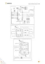
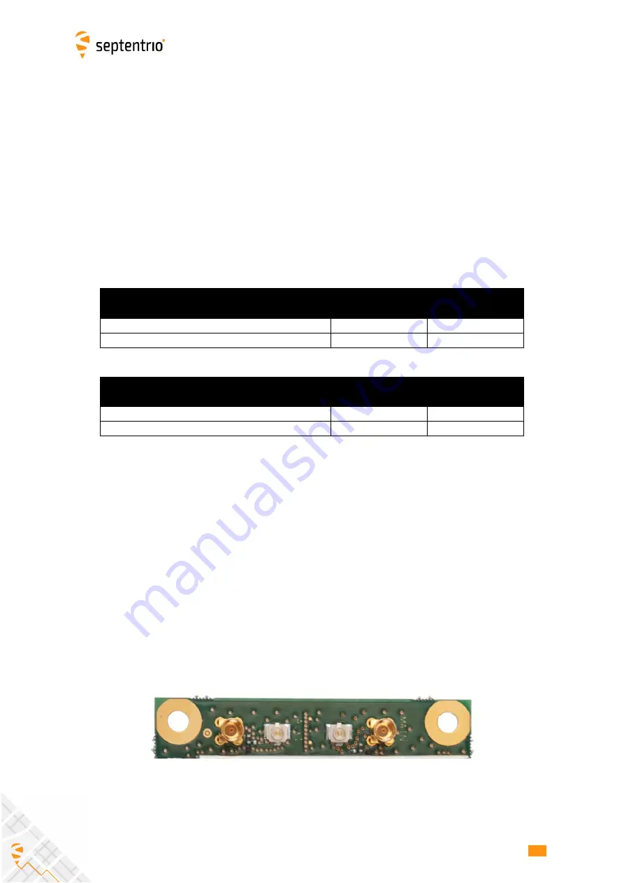
For illustration purposes, the above picture shows both u.FL and MMCX connectors. In 
reality, only one type of connector is available depending on the board variant. 
   

AUX1


MAIN


Summary of Contents for AsteRx-i3

Page 1: ...AsteRx i3 Product Group Hardware Manual Version 1 0 0 ...

Page 2: ...ware Manual Version 1 0 0 April 9 2021 Copyright 2000 2021 Septentrio nv sa All rights reserved Septentrio Greenhill Campus Interleuvenlaan 15i 3001 Leuven Belgium http www septentrio com Phone 32 16 300 800 Fax 32 16 221 640 septentrio ...

Page 3: ...tors 11 2 7 1 30 pin Connector 12 2 7 2 60 pin connector 13 2 8 Frequency Reference Output REF OUT 15 2 9 Event TimeSync Inputs 15 2 10 General Purpose Output GPx 15 2 11 Standby Mode 15 2 12 SD Memory Card Usage 16 2 13 USB Interface 17 2 14 Ethernet 17 2 15 ADIS IMU AsteRx i3 D OEM only 19 2 15 1 IMU Frame and Reference Point 19 2 15 2 IMU Orientation in Vehicle 19 3 ELLIPSE2 MICRO FROM SBG SYST...

Page 4: ... KIT 30 5 1 Header Types 30 5 2 Powering the DevKit 30 5 3 Antenna Connectors 31 5 4 LEDs and General Purpose Output Pins 32 5 5 COM Ports 32 5 6 PPS Out and Event Inputs 33 5 7 Ethernet 34 5 8 USB Dev 34 5 9 USB Host 34 5 10 REF IN 34 5 11 Buttons 34 5 12 SD Card Socket 35 5 13 Connection with the Ellipse2 IMU 35 APPENDIX A LED STATUS INDICATORS 36 APPENDIX B SYSTEM NOISE FIGURE AND C N0 38 APPEN...

Page 5: ...o see www septentrio com en environmental compliance ESD PRECAUTIONS The OEM module is sensitive to electrostatic discharge ESD Although it has a limited protection it should only be manipulated in an ESD safe environment and using ESD safe tools and equipment These tools are typically marked with the following symbol ...

Page 6: ...6 6 AsteRx i3 D OEM AsteRx i3 S OEM 6 2 AsteRx i3 D OEM AsteRx i3 S OEM 2 1 AsteRx i3 D OEM All dimensions in millimeters Weight 29 g AUX1 MAIN REF OUT ...

Page 7: ...ard but it does not incorporate the ADIS IMU It is designed to operate with an external SBG Ellipse IMU see chapter 3 All dimensions in millimeters Weight 27 g Note the above pictures and mechanical diagrams show both u FL and MMCX antenna connectors In reality only one type of connector is available depending on the board variant AUX1 MAIN REF OUT ...

Page 8: ...y be connected to ground on the host PCB Note however that the mounting holes should not be relied on as only ground return connection a proper ground should be supplied to the GND pins of the I O connector s as well The maximum height of the components at the bottom side of the AsteRx i3 OEM board is within the mask shown below applicable to both AsteRx i3 D OEM and AsteRx i3 S OEM The maximum co...

Page 9: ...ations 1 80 W 1 20 W AsteRx i3 S OEM excluding SBG IMU add 400mW to include it Signals enabled with setSignalTracking Power consumption Dual antenna Single antenna GPS L1 L2 GLO L1 L2 1 15 W 0 80 W All GNSS signals from all GNSS constellations 1 60 W 1 00 W Enabling the built in L Band demodulator with the setLBandSelectMode command adds 100 mW Enabling wideband interference mitigation with the se...

Page 10: ...na current limit 150 mA per antenna Antenna net gain range1 15 50 dB For optimal performances the net gain on MAIN and AUX1 must not differ by more than 10dB Receiver noise figure 10 dB with 15 dB net gain The receiver noise figure increases as the net gain increases but its contribution to the system noise figure decreases The worse case is for a net gain of 15dB RF nominal input impedance 50 Ohm...

Page 11: ...at connector is not used Do not drive a non zero voltage into input pins pins type I in the tables below when the receiver is not powered In addition if standby mode is applicable input pins must remain in high Z when the IO_EN signal is not set See section 2 11 for details When pull up down resistors are needed use 10 k Unused or reserved pins should be left unconnected unless explicitly mentione...

Page 12: ...cator Max output current 10 mA output impedance 20 Ohms See Appendix A 29 GND Gnd 0 Ground Pin Name Type Level Description Comment 2 Vin P 3 3V 5 Main power supply input Both Vin pins pin 1 and pin 2 must be tied together 4 GND Gnd 0 Ground 6 USB_D I O USB USB data signal negative D 8 nRST Ctrl PU LVTTL Reset input active negative Receiver resets when driven low 10 RX1 I K LVTTL Serial COM 1 recei...

Page 13: ...15 TX4 O LVTTL Serial COM 4 transmit line inactive state is high 17 Reserved 19 Reserved 21 Reserved 23 Reserved 25 Reserved 27 Reserved 29 GND Gnd Ground 31 RMII_TXEN O LVTTL LAN PHY transmit enable See section 2 14 33 RMII_TXD1 O LVTTL LAN PHY transmit data 1 See section 2 14 35 RMII_CRS_DV I LVTTL LAN PHY CRS See section 2 14 37 RMII_RXER I LVTTL LAN PHY RX error See section 2 14 39 Reserved 41...

Page 14: ...nd Ground 20 Reserved 22 Reserved 24 Reserved 26 Reserved 28 Reserved 30 GND Gnd Ground 32 RMII_CLK O LVTTL LAN PHY Clock See section 2 14 34 RMII_TXD0 O LVTTL LAN PHY transmit data 0 See section 2 14 36 GND Gnd Ground 38 RMII_RXD0 I LVTTL LAN PHY receive data 0 See section 2 14 40 RMII_RXD1 I LVTTL LAN PHY receive data 1 See section 2 14 42 GND Gnd Ground 44 GP2 O LVTTL General purpose output GP2...

Page 15: ...general purpose LVTTL digital outputs of which the level can be programmed with the setGPIOFunctionality command During the first seconds after powering up the board these pins are in tristate Use an external pull down or pull up resistor to have the desired level during boot The GPx pins can drive a maximum current of 10mA 2 11 Standby Mode In standby mode all receiver functions are turned off an...

Page 16: ...fer mode with 3V3 signaling An example circuit to a 9 pin SD memory card socket is shown below The maximum clock frequency SD_CLK is 33 000 MHz See instructions in the Reference Guide for details on how to configure SD card logging The receiver is compatible with SD cards of up to 32GB The file system is FAT32 Shortly driving the button pin pin 25 of 30 pin connector low toggles logging on and off...

Page 17: ...iles AsteRx i3_USB_1_1 suf and AsteRx i3_USB_2_0 suf located in the USB folder of the firmware package can be used to change this The current USB mode can be checked with the command lif Identification 2 14 Ethernet The receiver supports full duplex 10 100 Base T Ethernet communication The Ethernet PHY and magnetics are to be implemented on the host board Connection with the PHY is through the RMI...

Page 18: ...18 18 AsteRx i3 D OEM AsteRx i3 S OEM 18 ...

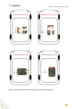
Page 19: ...Reference Point The IMU reference point is the bottom corner of the ADIS16505 package at the edge marked by the hole in the top of the lid as illustrated below 2 15 2 IMU Orientation in Vehicle The orientation of the AsteRx i3 D OEM in your vehicle must be provided to the receiver using the setIMUOrientation command Selected examples are shown below X Y ...

Page 20: ...20 20 AsteRx i3 D OEM AsteRx i3 S OEM 20 Refer to the Reference Guide to configure the INS GNSS integration ...

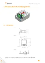
Page 21: ...21 21 Ellipse2 Micro from SBG Systems 21 3 Ellipse2 Micro from SBG Systems 3 1 Dimensions All dimensions in mm The IMU reference point is marked by the symbol ...

Page 22: ...r is Harwin G125 3041096L4 plus contacts The input voltage range VIN pin is from 4 to 15V Communication with the AsteRx i3 S OEM module is through Port A 3 4 Open Ended Cable Septentrio s CBL_AxiS_OEM_IMU cable part 215684 can be used to connect the SBG IMU to the AsteRx i3 S OEM Twisted pairs are used when applicable to prevent cross talk between digital signals The wiring diagram and the wire co...

Page 23: ...pin connector Conversion from RS 232 to TTL level is needed COM3 is the default IMU port If using another port than COM3 it must be specified to the firmware with the setIMUInput command The SYNC A pin of the IMU must be connected to the PPSout pin of the AsteRx i3 S OEM pin 12 of the 30 pin connector The PPSout rate must be left at its default value 1Hz ...

Page 24: ...terface Board is an interface card designed to ease integration and test This chapter provides information on the interface card only Refer to chapter 2 for the specifications of the AsteRx i3 OEM board LOG button AsteRx i3 OEM Interface board USB Dev Power PPS Event 44 pin IO ...

Page 25: ...gs The drawing below shows the dimension of the Interface Board attached to the AsteRx i3 D OEM Weight 52g 4 2 USB Dev Connector type micro USB type B That connector can be attached to a PC to power the receiver and to communicate with it over its USB port ...

Page 26: ... Pulse per second output of the OEM receiver also used as synchronization signal for the IMU Also available on the 6 pin header see 4 6 14 Reserved 15 EVENTA1 I PD EventA input 5V tolerant The logical level on EVENTA1 and EVENTA2 pins are ORed before being transferred to the EVENTA pin of the AsteRx i3 OEM EVENTA2 available on the 6 pin header see 4 6 16 Reserved 17 COM2_CTS I PU LVTTL COM2 cleare...

Page 27: ...onnection 43 PWR_IN P 4 5 30V Power input See section 4 7 44 PWR_IN P 4 5 30V Power input See section 4 7 Note 1 The level of the GP1 pin of the AsteRx i3 OEM pin 9 of the 60 pin connector see 2 7 2 must be low for the EVENT pins to be functional Note 2 On board magnetics The Ethernet pins can directly be routed to an Ethernet connector 4 4 LEDs The GP2 LED reflects the status of the GP2 pin pin 4...

Page 28: ...S signal at different electrical levels Pin name Level during pulse Level outside pulse 5V_PPS 5V 0V 3V3_PPS 3 3V 0V OpDrain_PPS 0V floating 3V3_INV_PPS 0V 3 3V The EVENTA2 pin is a second input for the EVENTA of the AsteRx i3 OEM see section 2 9 The first input pin EVENTA1 is available on the 44 pin connector The EVENTA input of the OEM receiver is the logical OR of EVENTA1 and EVENTA2 4 7 Power ...

Page 29: ...ctor see section 4 3 The voltage range when powering from the PWR_IN pins is 4 5V to 30V Power can be applied from both sources at the same time On board diodes prevent short circuits The interface board provides the 3V3 supply to the AsteRx i3 OEM receiver and a 5V DC voltage to the VANT pin of the AsteRx i3 OEM ...

Page 30: ...it 1 From the USB Dev connector J205 This allows powering the board from a PC or from a standard phone charger adapter The supported USB voltage range is 4 5V 5 5V 2 Using the POWER connector J203 The supported voltage range is 5 36V When powering from the USB Dev connector it is recommended to use the USB cable provided with the DevKit Low quality USB cables often suffer from excessive voltage dr...

Page 31: ...connect the two pins to the probes of a multimeter in current sensing mode Measure the current flowing between the two pins and multiply it by 3 3V to obtain the power consumption It is recommended to set the multimeter in high ampere setting to keep the voltage drop as low as possible 5 3 Antenna Connectors There is no antenna connector on the DevKit The antennas must be connected directly to the...

Page 32: ...s of the 30 pin connector of the AsteRx i3 OEM board See section 2 7 1 for the pinout and Appendix A for a description of the LED behavior The 3 3V GP1 and GP2 outputs are available on the J501 header 5 5 COM Ports By default the four COM ports of the AsteRx i3 OEM are routed to the four DB9 connectors Electrical levels on the BD9 conform to the RS232 standard RTS CTS lines are supported only on C...

Page 33: ...ors using the RS232 levels Note that when using the DB9 connectors the baud rate must not be larger than 230400baud This limitation does not apply to the TTL signals 5 6 PPS Out and Event Inputs The PPSout pin of header J500 is directly connected to the PPSOut pin of the AsteRx i3 OEM see section 2 7 1 The PPS level is 3 3V The EVENTA and EVENTB pins of J500 are connected to the EventA and EventB ...

Page 34: ...Reserved 5 10 REF IN Reserved 5 11 Buttons Pressing the nRST button drives the nRST pin of the AsteRx i3 OEM low which resets the receiver Pressing the LOGGING button drives the Button pin of the AsteRx i3 OEM low This can be used to enabled and disable logging as described in section 2 12 The buttons are also connected to J601 and J602 2 pin headers see above picture Tying the nRST or LOGGING pin...

Page 35: ...ection 2 12 for a description of the SD Card logging 5 13 Connection with the Ellipse2 IMU Septentrio s open ended SBG IMU cable see sections 3 4 can be used to connect the DevKit to the Ellipse2 IMU The following connections are recommended 5V out to Ellipse2 VIN PPS out to Ellipse2 SYNC A COM3 to Ellipse2 PORT A ...

Page 36: ...or which differential corrections have been provided in the last received differential correction message RTCM or CMR LED behaviour Number of satellites with corrections LED is off No differential correction message received blinks fast and continuously 10 times per second 0 blinks once then pauses 1 2 blinks twice then pauses 3 4 blinks 3 times then pauses 5 6 blinks 4 times then pauses 7 8 blink...

Page 37: ... activity LED LED Behaviour LOGLED LED is off when the SD card is not present or not mounted LED is on when the SD card is present and mounted Short blinks indicate logging activity During boot i e during the first seconds after powering the receiver the state of the LEDs is not defined ...

Page 38: ...A noise figure 30 dB antenna LNA gain and 15 dB cable loss Gpreamp 30dB 15dB 15dB In this case the system noise figure is NFsys 10 log10 102 5 10 1010 10 1 1015 10 3 14 dB The C N0 in dB Hz of a GNSS signal received at a power P can be computed by C N0 P 10 log10 Tant 290 10NFsys 10 1 228 6 dB where P is the received GNSS signal power including the gain of the antenna passive radiating element in ...

Page 39: ...nditions the C N0 values should reach up to 50 dB Hz for the strong signals on L1 and up to 45 dB Hz on L2 as illustrated below If the maximum C N0 is lower than expected interference and cross talk from nearby electronics is likely and the source of the problem needs to be identified This is where the RF spectrum monitor built in the receiver comes in handy The spectrum monitor can be accessed in...

Page 40: ...band and slightly degrades the L1 C N0 of some GLONASS satellites Try to keep personal computers and other equipment more than 2 meters away from the antenna while assessing electromagnetic compatibility of the integration RxControl also allows to observe the time domain signal This should look like white Gaussian noise as illustrated below ...

Page 41: ... the system frequencies For example peaks at 1200 and 1248 MHz are an indication of an interfering source at 48 MHz as this maps to the 25th and 26th harmonic of a 48 MHz signal This may correspond to the frequency of a microcontroller in the application Integration cross talk can be solved in a number of ways Shift the clock frequency of the interfering signal to avoid the GNSS bands Use shieldin...

Reviews: