background image

29


29


Development Kit 


29


4.7


Ethernet 

The  DevKit  supports  10/100  Base-T  Ethernet.      It  is  not  possible  to  power  the  DevKit 
through the Ethernet connector.


4.8


USB Dev 

That connector can be attached to a PC to power the DevKit and to communicate with the 
receiver over its USB port. 

4.9


USB Host 

Reserved. 


4.10


REF IN 

The REF IN connector can be used to feed the receiver with an external 10-MHz sinusoidial 
frequency reference.  See section 2.6. 
 
Input impedance: 

50 

Input level:   

between -10dBm and +14dBm (0.2Vpp to 3.2Vpp). 


4.11


Buttons 


Pressing  the  nRST  button  drives  the  nRST  pin  of  the  AsteRx-m3  low,  which  resets  the 
receiver.  
 
Pressing the LOGGING button drives the Button pin of the AsteRx-m3 low.  This can be 
used to enabled and disable logging, as described in section 2.11.  
 
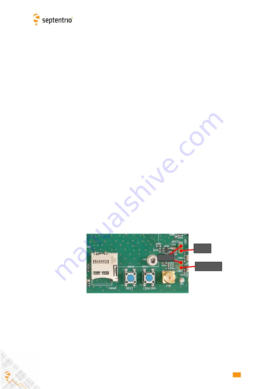
The buttons are also connected to J601 and J602 2-pin headers (see above picture).   Tying 
the  nRST  or  LOGGING  pins  of  these  headers  to  ground  is  the  same  as  pressing  the 
respective button. 


nRST


LOGGING


GND


Summary of Contents for AsteRx-m3

Page 1: ...AsteRx m3 Product Group Hardware Manual Version 2 2 0 ...

Page 2: ...ware Manual Version 2 2 0 May 28 2021 Copyright 2000 2021 Septentrio nv sa All rights reserved Septentrio Greenhill Campus Interleuvenlaan 15i 3001 Leuven Belgium http www septentrio com Phone 32 16 300 800 Fax 32 16 221 640 septentrio ...

Page 3: ...60 pin connector 12 2 6 External Frequency Reference Input REF IN 14 2 7 Frequency Reference Output REF OUT 14 2 8 Event TimeSync Inputs 14 2 9 General Purpose Output GPx 15 2 10 Standby Mode 15 2 11 SD Memory Card Usage 16 2 12 USB Interface 17 2 13 Ethernet 17 3 ROBOTICS INTERFACE BOARD 19 3 1 Mechanical Drawings 20 3 2 USB Dev 20 3 3 44 pin Header 21 3 4 LEDs 22 3 5 Log Button Header 23 3 6 PPS...

Page 4: ...4 LEDs and General Purpose Output Pins 27 4 5 COM Ports 27 4 6 PPS Out and Event Inputs 28 4 7 Ethernet 29 4 8 USB Dev 29 4 9 USB Host 29 4 10 REF IN 29 4 11 Buttons 29 4 12 SD Card Socket 30 APPENDIX A LED STATUS INDICATORS 31 APPENDIX B SYSTEM NOISE FIGURE AND C N0 33 APPENDIX C EMC CONSIDERATIONS 34 ...

Page 5: ...o see www septentrio com en environmental compliance ESD PRECAUTIONS The OEM module is sensitive to electrostatic discharge ESD Although it has a limited protection it should only be manipulated in an ESD safe environment and using ESD safe tools and equipment These tools are typically marked with the following symbol ...

Page 6: ...and mechanical diagrams show both u FL and MMCX antenna connectors In reality only one type of connector is available depending on the board variant RF connectors u FL or MMCX type are mounted on top side of the PCB The 30 and 60 pin Hirose I O connectors are mounted on the bottom side AUX1 MAIN REF OUT ...

Page 7: ... ground should be supplied to the GND pins of the I O connector s as well The maximum height of the components at the bottom side of the AsteRx m3 OEM board is within the mask shown below The maximum component height is 1 1mm in the green area and 1 6mm in the yellow area 2 2 Environmental Operational 40 to 85 C Storage 55 to 85 C 2 3 Power and Power Consumption The board is powered through pin 1 ...

Page 8: ... consumption in the above table are average values To account for peak currents the minimum power supply drive capability should be 1 Ampere 2 4 RF Interface For illustration purposes the above picture shows both u FL and MMCX connectors In reality only one type of connector is available depending on the board variant The main antenna must be connected to the u FL or MMCX connector marked MAIN on ...

Page 9: ... the system noise figure decreases The worse case is for a net gain of 15dB RF nominal input impedance 50 Ohms VSWR 2 5 1 in 1200 1251 MHz and 1560 1610 MHz range 1 The net gain is the total pre amplification of the distribution network in front of the receiver Typically this equals antenna active LNA gain minus coax losses in the applicable GNSS bands ...

Page 10: ...tor is not used Do not drive a non zero voltage into input pins pins type I in the tables below when the receiver is not powered In addition if standby mode is applicable input pins must remain in high Z when the IO_EN signal is not set See section 2 10 for details When pull up down resistors are needed use 10 k Unused or reserved pins should be left unconnected unless explicitly mentioned otherwi...

Page 11: ...terpreted as button pressed Debouncing must be done externally no debouncing circuit on board See also section 2 11 27 LOGLED O LVTTL Internal logging status indicator Max output current 10 mA output impedance 20 Ohms See Appendix A 29 GND Gnd 0 Ground Pin Name Type Level Description Comment 2 Vin P 3 3V 5 Main power supply input Both Vin pins pin 1 and pin 2 must be tied together 4 GND Gnd 0 Grou...
Page 12: ...L Serial COM 4 transmit line inactive state is high 17 Reserved 19 Reserved 21 Reserved 23 Reserved 25 Reserved 27 Reserved 29 GND Gnd Ground 31 RMII_TXEN O LVTTL LAN PHY transmit enable See section 2 13 33 RMII_TXD1 O LVTTL LAN PHY transmit data 1 See section 2 13 35 RMII_CRS_DV I LVTTL LAN PHY CRS See section 2 13 37 RMII_RXER I LVTTL LAN PHY RX error See section 2 13 39 Reserved 41 Reserved 43 ...

Page 13: ...8 Reserved 30 GND Gnd Ground 32 RMII_CLK O LVTTL LAN PHY Clock See section 2 13 34 RMII_TXD0 O LVTTL LAN PHY transmit data 0 See section 2 13 36 GND Gnd Ground 38 RMII_RXD0 I LVTTL LAN PHY receive data 0 See section 2 13 40 RMII_RXD1 I LVTTL LAN PHY receive data 1 See section 2 13 42 GND Gnd Ground 44 GP2 O LVTTL General purpose output GP2 in setGPIOFunctionality command See section 2 9 46 Reserve...

Page 14: ...put REF OUT The frequency reference used by the receiver is available at the REFOUT u FL connector This is a 10MHz square wave 0 2 8V output impedance 50Ohms The REFOUT signal can be enabled or disabled with the setREFOUTMode command It is enabled by default When an external frequency reference is provided to the REF IN pin see section 2 6 the signal at the REF OUT connector is synchronized with t...

Page 15: ... these pins are in tristate Use an external pull down or pull up resistor to have the desired level during boot The GPx pins can drive a maximum current of 10mA 2 10 Standby Mode In standby mode all receiver functions are turned off and the power consumption is significantly reduced see section 2 3 There are two ways to enter standby mode 1 By driving the nPDN pin low pin 20 of the 30 pin connecto...

Page 16: ...e file system is FAT32 Shortly driving the button pin pin 25 of 30 pin connector low toggles logging on and off Driving the button pin low for at least 5 seconds unmounts the SD card if it was mounted or mounts it if it was unmounted The SD card mount status can be checked with the LOGLED pin see Appendix A When powering off the receiver while logging is ongoing it can be that the last seconds of ...

Page 17: ...age can be used to change this The current USB mode can be checked with the command lif Identification 2 13 Ethernet The receiver supports full duplex 10 100 Base T Ethernet communication The Ethernet PHY and magnetics are to be implemented on the host board Connection with the PHY is through the RMII interface available on the 60 pin connector An example of application circuit using the ksz8041 P...

Page 18: ...18 18 AsteRx m3 OEM 18 ...

Page 19: ...s of an AsteRx m3 OEM board mounted on an interface card designed to ease integration and test This chapter provides information on the interface card only Refer to chapter 2 for the specifications of the AsteRx m3 OEM board LOG button AsteRx m3 OEM Interface board USB Dev Power PPS Event 44 pin IO ...

Page 20: ...botics Interface Board 20 3 1 Mechanical Drawings Weight 50g 3 2 USB Dev Connector type micro USB type B That connector can be attached to a PC to power the receiver and to communicate with it over its USB port ...

Page 21: ...1PPS_OUT O LVTTL First pulse per second output PPS1 of the OEM receiver Also available on the 6 pin header see 3 6 14 Reserved 15 EVENTA1 I PD LVTTL EventA input 5V tolerant The logical level on EVENTA1 and EVENTA2 pins are ORed before being transferred to the EVENTA pin of the AsteRx m3 OEM EVENTA2 available on the 6 pin header see 3 6 16 Reserved 17 COM2_CTS I PU LVTTL COM2 cleared to send input...

Page 22: ...onnection 43 PWR_IN P 4 5 30V Power input See section 3 7 44 PWR_IN P 4 5 30V Power input See section 3 7 Note 1 The level of the GP1 pin of the AsteRx m3 OEM pin 9 of the 60 pin connector see 2 5 2 must be low for the EVENT pins to be functional Note 2 On board magnetics The Ethernet pins can directly be routed to an Ethernet connector 3 4 LEDs The GP2 LED reflects the status of the GP2 pin pin 4...

Page 23: ...S signal PPS1 at different electrical levels Pin name Level during pulse Level outside pulse 5V_PPS 5V 0V 3V3_PPS 3 3V 0V OpDrain_PPS 0V floating 3V3_INV_PPS 0V 3 3V The EVENTA2 pin is a second input for the EVENTA of the AsteRx m3 OEM see section 2 8 The first input pin EVENTA1 is available on the 44 pin connector The EVENTA input of the OEM receiver is the logical OR of EVENTA1 and EVENTA2 3 7 P...

Page 24: ...ctor see section 3 3 The voltage range when powering from the PWR_IN pins is 4 5V to 30V Power can be applied from both sources at the same time On board diodes prevent short circuits The interface board provides the 3V3 supply to the AsteRx m3 OEM receiver and a 5V DC voltage to the VANT pin of the AsteRx m3 OEM ...

Page 25: ... two ways to power the DevKit 1 From the USB Dev connector J205 This allows powering the board from a PC or from a standard phone charger adapter The supported USB voltage range is 4 5V 5 5V 2 Using the POWER connector J203 The supported voltage range is 5 36V When powering from the USB Dev connector it is recommended to use the USB cable provided with the DevKit Low quality USB cables often suffe...

Page 26: ...connect the two pins to the probes of a multimeter in current sensing mode Measure the current flowing between the two pins and multiply it by 3 3V to obtain the power consumption It is recommended to set the multimeter in high ampere setting to keep the voltage drop as low as possible 4 3 Antenna Connectors There is no antenna connector on the DevKit The antennas must be connected directly to the...

Page 27: ... pins of the 30 pin connector of the AsteRx m3 board See section 2 5 1 for the pinout and Appendix A for a description of the LED behavior The 3 3V GP1 and GP2 outputs are available on the J501 header 4 5 COM Ports By default the four COM ports of the AsteRx m3 are routed to the four DB9 connectors Electrical levels on the BD9 conform to the RS232 standard RTS CTS lines are supported only on COM2 ...

Page 28: ...t when using the DB9 connectors the baud rate must not be larger than 230400baud This limitation does not apply to the TTL signals 4 6 PPS Out and Event Inputs The PPSout pin of header J500 is directly connected to the PPS1 pin of the AsteRx m3 see section 2 5 1 The PPS level is 3 3V The EVENTA and EVENTB pins of J500 are connected to the EventA and EventB pins of the AsteRx m3 through a buffer Th...

Page 29: ...l 10 MHz sinusoidial frequency reference See section 2 6 Input impedance 50 Input level between 10dBm and 14dBm 0 2Vpp to 3 2Vpp 4 11 Buttons Pressing the nRST button drives the nRST pin of the AsteRx m3 low which resets the receiver Pressing the LOGGING button drives the Button pin of the AsteRx m3 low This can be used to enabled and disable logging as described in section 2 11 The buttons are al...

Page 30: ...30 30 Development Kit 30 4 12 SD Card Socket The receiver can log files on the micro SD Card in this socket See section 2 11 for a description of the SD Card logging ...

Page 31: ...or which differential corrections have been provided in the last received differential correction message RTCM or CMR LED behaviour Number of satellites with corrections LED is off No differential correction message received blinks fast and continuously 10 times per second 0 blinks once then pauses 1 2 blinks twice then pauses 3 4 blinks 3 times then pauses 5 6 blinks 4 times then pauses 7 8 blink...

Page 32: ... activity LED LED Behaviour LOGLED LED is off when the SD card is not present or not mounted LED is on when the SD card is present and mounted Short blinks indicate logging activity During boot i e during the first seconds after powering the receiver the state of the LEDs is not defined ...

Page 33: ...A noise figure 30 dB antenna LNA gain and 15 dB cable loss Gpreamp 30dB 15dB 15dB In this case the system noise figure is NFsys 10 log10 102 5 10 1010 10 1 1015 10 3 14 dB The C N0 in dB Hz of a GNSS signal received at a power P can be computed by C N0 P 10 log10 Tant 290 10NFsys 10 1 228 6 dB where P is the received GNSS signal power including the gain of the antenna passive radiating element in ...

Page 34: ...nditions the C N0 values should reach up to 50 dB Hz for the strong signals on L1 and up to 45 dB Hz on L2 as illustrated below If the maximum C N0 is lower than expected interference and cross talk from nearby electronics is likely and the source of the problem needs to be identified This is where the RF spectrum monitor built in the receiver comes in handy The spectrum monitor can be accessed in...

Page 35: ...band and slightly degrades the L1 C N0 of some GLONASS satellites Try to keep personal computers and other equipment more than 2 meters away from the antenna while assessing electromagnetic compatibility of the integration RxControl also allows to observe the time domain signal This should look like white Gaussian noise as illustrated below ...

Page 36: ... and the system frequencies For example peaks at 1200 and 1248 MHz are an indication of an interfering source at 48 MHz as this maps to the 25th and 26th harmonic of a 48 MHz signal This may correspond to the frequency of a microcontroller in the application Integration cross talk can be solved in a number of ways Shift the clock frequency of the interfering signal to avoid the GNSS bands Use shie...

Reviews: