background image

1

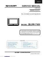
28JW-74H

      MODEL 

28JW-74H

 PAL I SYSTEM COLOUR TELEVISION

SE

00

28JW74H00

SERVICE MANUAL


  Issued:21

st

 June  2002

This document has been published to
 be used for after sales service only.

  GA-20

 CHASSIS

In the interests of user safety (required by safety
regulations in some countries) the set should restored
to its original condition and only parts identical to
those specified should be used.

CONTENTS

ELECTRICAL SPECIFICATIONS ................... 3
IMPORTANT SERVICING NOTES ................. 4
CONTROLS & TERMINALS ........................... 5
ADJUSTMENT PROCEDURES ...................... 7
POSTCODE RESET ...................................... 11
LED FLASHING CODES ............................... 12
PRINTED WIRING BOARDS ........................ 13

CHASSIS LAYOUT ......................................... 19
ICs ADDITIONAL INFORMATION .................. 21
SCHEMATIC DIAGRAMS ............................... 36
TROUBLESHOOTING TABLES ..................... 49
PARTS LISTING ............................................. 52
SOURCE OF DOCUMENTATION .................. 60
PACKING OF THE SET & ACCESSORIES ... 61

SHARP  CORPORATION

8

Summary of Contents for 28JW-74H

Page 1: ...the set should restored to its original condition and only parts identical to those specified should be used CONTENTS ELECTRICAL SPECIFICATIONS 3 IMPORTANT SERVICING NOTES 4 CONTROLS TERMINALS 5 ADJUSTMENT PROCEDURES 7 POSTCODE RESET 11 LED FLASHING CODES 12 PRINTED WIRING BOARDS 13 CHASSIS LAYOUT 19 ICs ADDITIONAL INFORMATION 21 SCHEMATIC DIAGRAMS 36 TROUBLESHOOTING TABLES 49 PARTS LISTING 52 SOU...

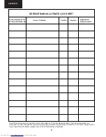
Page 2: ...f only part number changes are required just change part number directly the part number in the Parts Listing Section If you need more information please refer to the Technical Report Bulletin SERVICE MANUAL UPDATE LOG SHEET Part No Technical Report No Technical Bulletin No Cause Solution Page No Application Data Serial No ...

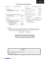
Page 3: ... exceed 15 of its original value X 0 290 0 015 Y 0 284 0 015 WARNING The chassis in this receiver is partially hot Use an isolation transformer between the line cord plug and power receptacle when servicing this chassis To prevent electric shock do not remove cover No user serviceable parts inside Refer servicing to qualified service personnel Specifications are subject to change without prior not...

Page 4: ...s x ray radiation levels This is a problem when in close proximity to the receiver for long periods of time To reduce any risks associated with this please observe the following precautions 1 When undertaking any servicing on this chassis DO NOT increase the EHT to more than 32 0 KV at a instantaneous beam current of 1500µA 2 Ensure that during normal operation the EHT does not exceed 29 5KV 1 5KV...

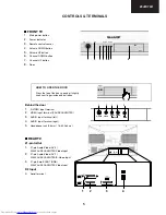
Page 5: ... 1 L S G I R D D D AUDIO S VIDEO VIDEO 5 FRONT REAR R R L L WOOFER AV 2 AV TERMINAL AV 1 AV TERMINAL RGB SCART PERITELEVISION 4 2 3 1 CONTROLS TERMINALS FRONT TV 1 Main power button 2 Power indicator 3 Remote control sensor 4 Volume DOWN button 5 Volume UP button 6 Channel DOWN button 7 Channel UP button 8 Door 2 3 4 5 6 7 1 8 Behind the door 1 S VIDEO input terminal 2 VIDEO input terminal PAL SEC...

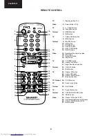
Page 6: ...8 Stop button TV 19 TV VIDEO button 20 Channel Call button 21 Single Double entry button Teletext 22 YELLOW button 23 BLUE button TV 24 Channel UP button 25 Volume UP button 26 Channel DOWN button 27 Wide mode button TV Teletext 28 CLOCK button TV 29 Sound mode button Teletext 30 HOLD button TV 31 Sound Mute button Teletext 32 TEXT MIX PICTURE button 33 INDEX button Video 34 Channel UP button VCR ...

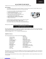
Page 7: ...XX The figures displayed in the XXXX locations are hexadecimal representations of the number of times that particular function has been executed For example if the hexadecimal number displayed after SW on was 0E4A this would correspond to the receiver being turned on 3658 times The figure displayed in the x location is the EPROM version Adjustment menu The following adjustments can be carried out ...

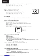
Page 8: ...by button on the remote control to store Pin Phase Adjust the Pin Phase so that the picture is symmetrical top and bottom The effect of this adjustment is shown in figure 4 When the volume up button is pressed side pincushion changes When the volume down button is pressed side pincushion changes Press the stand by button on the remote control to store Pin Amp Adjust the Pin Amp so that the picture...

Page 9: ...figure 9 When the volume up button is pressed the vertical angle changes to right When the volume down button is pressed the vertical angle changes to left Press the stand by button on the remote control to store Vertical Bow Adjust the Vertical Bow so that the picture is centred The effect of this adjustment is shown in figure 10 When the volume up button is pressed the vertical bow changes to ri...

Page 10: ... 290 0 015 Y 0 284 0 015 To increase press volume up button and to decrease press volume down button RED CUT OFF alter X coordinate GREEN CUT OFF alter Y coordinate BLUE CUT OFF alter X and Y coordinate 3 Follow the procedure below to set the GAIN 3 1 Using brightness and contrast buttons select a luminance of 100 NITS 3 2 Operate in Service Mode and select location RED GAIN GREEN GAIN and BLUE GA...

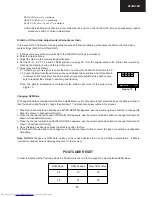
Page 11: ...e data to be adjusted is contained at the bottom right corner of the picture See Figure 15 Changing NVM Data To change the data contained within the Non Volatile Memory it is necessary to first select the page the data is stored in then the position and finally to change the data itself The procedure below outlines this process 1 Press the channel up down buttons and ALTER NVM PAG appears use the ...

Page 12: ...erator on CH12 2 Adjust the signal strength of the pattern generator to 59dB µV 75Ω 3 Enter the Service Mode 4 Enter the AGC Adjustment menu 5 Press the stand by button on the remote control 6 The adjustment will be carried out and stored automatically Auto Installation On Off To return the receiver to the original Auto Installation mode using the volume up or down button set the Auto Installation...

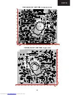
Page 13: ...3 28JW 74H FB218WJN2 CRT UNIT PWB Component side FB218WJN2 CRT UNIT PWB Copper side 11 1 2 3 4 5 6 7 8 9 10 Y X 0 10 11 12 13 1 2 3 4 5 6 7 8 9 Y X 11 1 2 3 4 5 6 7 8 9 10 0 10 9 8 7 6 5 4 3 2 1 13 12 11 ...

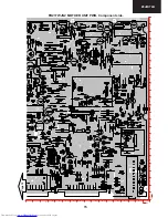
Page 14: ...14 28JW 74H 22 23 24 25 17 18 19 20 21 11 12 13 14 15 16 1 2 3 4 5 6 7 8 9 10 Y X 0 10 11 12 13 14 15 16 17 1 2 3 4 5 6 7 8 9 Page 15 FB217WJN2 MOTHER UNIT PWB Component side ...

Page 15: ...15 28JW 74H FB217WJN2 MOTHER UNIT PWB Component side Page 14 29 30 31 32 33 20 21 22 23 24 25 26 27 28 17 18 19 Y X 22 23 24 25 17 18 19 20 21 11 12 13 14 15 16 1 2 3 4 5 6 7 8 9 10 16 ...

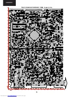
Page 16: ...16 28JW 74H 22 23 24 25 17 18 19 20 21 11 12 13 14 15 16 1 2 3 4 5 6 7 8 9 10 Y FB217WJN2 MOTHER UNIT PWB Copper side Page 17 19 18 17 16 29 28 27 26 25 24 23 22 21 20 33 32 31 30 X ...

Page 17: ...17 28JW 74H FB217WJN2 MOTHER UNIT PWB Copper side Page 16 22 23 24 25 17 18 19 20 21 11 12 13 14 15 16 2 3 4 5 6 7 8 9 10 1 Y X 0 10 9 8 7 6 5 4 3 2 1 17 16 15 14 13 12 11 ...

Page 18: ...CONTROL UNIT PWB Component side Copper side Y X 22 23 24 25 17 18 19 20 21 11 12 13 14 15 16 1 2 3 4 5 6 7 8 9 10 0 9 8 7 6 5 4 3 2 1 22 23 24 25 17 18 19 20 21 11 12 13 14 15 16 1 2 3 4 5 6 7 8 9 10 Y X 0 1 2 3 4 5 6 7 8 9 ...

Page 19: ...19 28JW 74H CHASSIS LAYOUT PWB A Mother Unit FB217N2 ...

Page 20: ...20 28JW 74H PWB B CHASSIS LAYOUT CRT SOCKET UNIT FB218N2 PWB C CHASSIS LAYOUT FRONTAL POWER CONTROL UNIT FB219N1 ...

Page 21: ...330 note 3 B G standard 5 L standard 7 ϕdif differential phase CCIR 330 2 4 deg Bvideo 1dB 1 dB video bandwidth trap bypass mode AC load CL 20 pF RL 1 kΩ 5 6 MHz Bvideo 3dB trap 3 dB video bandwidth including sound carrier trap note 4 ftrap 4 5 MHz 3 95 4 05 MHz ftrap 5 5 MHz 4 90 5 00 MHz ftrap 6 0 MHz 5 40 5 50 MHz ftrap 6 5 MHz 5 50 5 95 MHz αSC1 trap attenuation at first sound carrier M N stan...

Page 22: ...F2 in dB 6 dB is the correction term of internal circuitry and 3 dB is the tolerance of video output and intercarrier output Vo intc rms 8 Pin REF is able to operate as a 1 pin crystal oscillator input as well as an external reference signal input e g from the tuning system BAF 3dB 3 dB AF bandwidth without de emphasis dependent on FM PLL filter 80 100 kHz S NW AF weighted signal to noise ratio of...

Page 23: ...16 15 16 21 23 4 2 10 9 11 10 12 11 18 20 20 22 2 31 1 30 18 17 7 8 3 5 4 6 external reference signal or 4 MHz crystal REF AFC AUD CVBS audio output video output 2 V p p 1 1 V p p without trap C AF SIOMAD SDA SCL MAD V P C AGC 6 12 13 14 17 19 25 28 29 32 13 n c AGND 7 5 DGND OUTPUT PORTS I 2 C BUS TRANSCEIVER 22 24 3 1 OP1 OP2 FMPLL DEEM AFD sound intercarrier output and MAD select FM PLL filter ...

Page 24: ...3 not connected n c 14 not connected TAGC 14 14 15 tuner AGC output REF 15 15 16 4 MHz crystal or reference signal input VAGC 16 VIF AGC for capacitor n c 16 17 not connected CVBS 17 17 18 composite video output n c 19 not connected AGND 18 18 20 analog ground VPLL 19 19 21 VIF PLL for loop filter VP 20 20 22 supply voltage AFC 21 21 23 AFC output OP2 22 22 24 output port 2 open collector n c 25 n...

Page 25: ...T BY MUTE NC VCC SIGN VREG VCC POW VCC VCC VCC VCC NEGATIVE SUPPLY NEGATIVE SUPPLY NEGATIVE SUPPLY PWM OUTPUT BOOTSTRAP DIODE ANODE BOOTSTRAP CAPACITOR NOT CONNECTED FEEDBACK INTEGRATING CAPACITANCE SETTING FREQUENCY RESISTOR SIGNAL GROUND INPUT ST BY MUTE CONTROL PIN NOT CONNECTED POSITIVE SIGNAL SUPPLY 10V INTERNAL REGULATOR POSITIVE POWER SUPPLY NEGATIVE SUPPLY TO BE CONNECTED TO PIN 16 VIA C5 ...

Page 26: ... 30 KΩ SVR Supply Voltage Rejection f 100Hz Vr 0 5 46 60 dB Tr Tf Rising and Falling Time 50 ns RDSON Power Transistor on Resistance 0 4 Ω FSW Switching Frequency 100 120 140 KHz FSW_OP Switching Frequency Operative Range 100 200 KHz BF Zero Signal Frequency Constant 1 4x10⁹ HzΩ RF Frequency Controller Resistor Range 7 12 14 KΩ MUTE STAND BY FUNCTIONS VST BY Stand by range 0 8 V VMUTE Mute Range 1...

Page 27: ...3 32 31 30 29 28 27 26 25 1 2 3 4 5 6 7 8 9 10 11 12 13 14 15 16 17 18 19 20 21 22 23 24 64 63 62 61 60 59 58 57 56 55 54 53 52 51 50 49 48 47 46 45 44 43 42 41 AVSUP AVSUP ANA_IN1 ANA_IN ANA_IN2 TESTEN XTAL_IN XTAL_OUT TP AUD_CL_OUT NC NC D_CTR_I O_1 D_CTR_I O_0 ADR_SEL STANDBYQ CAPL_M AHVSUP CAPL_A SC1_OUT_L SC1_OUT_R VREF1 SC2_OUT_L SC2_OUT_R NC NC DACM_SUB NC DACM_L DACM_R VREF2 DACA_L NC AVSS...

Page 28: ...V dVSUP23 Voltage between AVSUP and DVSUP AVSUP DVSUP 0 5 0 5 V PTOT Power Dissipation PSDIP64 PSDIP52 PQFP80 PLQFP64 AHVSUP DVSUP AVSUP 1300 1200 1000 960 mW mW mW mW VIdig Input Voltage all Digital Inputs 0 3 VSUP2 0 3 V IIdig Input Current all Digital Pins 20 20 mA1 VIana Input Voltage all Analog Inputs SCn_IN_s 2 MONO_IN 0 3 VSUP1 0 3 V IIana Input Current all Analog Inputs SCn_IN_s 2 MONO_IN ...

Page 29: ...Voltage all Inputs 0 3 VSUPx 0 31 V VO Output Voltage all Outputs 0 3 VSUPx 0 31 V VIO Input Output Voltage all Open Drain Out puts 0 3 6 V VCT3834 IC1001 Fig 1 2 Block diagram of the VCT 38xxA B shaded blocks are optional The block diagram does not show the additional features of VCT 38xxB Video Front end Comb Filter Color Decoder Display Processor Video Back end Panorama Scaler 4 3 4 12 31 2 I2 ...

Page 30: ... 24 96 95 94 93 92 91 90 89 88 87 86 85 84 83 82 81 80 79 78 77 76 75 74 73 25 26 27 28 29 30 31 32 ADB7 ADB6 ADB5 VSUPADB ADB1 ADB0 DB0 DB1 DB2 DB3 VSUPDB GNDDB DB4 DB5 DB6 DB7 ADB2 ADB3 ADB4 GNDADB 72 71 70 69 68 67 66 65 49 CIN1 50 CIN2 CRIN 51 VIN1 52 VIN2 53 VIN3 54 VIN4 55 DISINTROM 56 P27 57 P26 58 P25 59 P24 60 VSUPP2 61 GNDP2 62 P23 63 P22 64 P21 97 VERTQ 98 VERT 99 EW 100 SENSE 101 GNDM ...

Page 31: ...Q Frequency setting resistor 11 SGND Signal Ground 12 IN Error amplifier inverting input 13 IN Error amplifier non inverting input 14 EA out Error amplifier output 15 VCC Positive supply 16 VCCPOW Positive Power supply 17 VccPOW Negative Power supply 18 VCC Negative supply 19 VCC Negative supply 20 VCC Negative supply STV9380 IC502 PIN CONNECTION 20 19 18 17 16 15 14 13 12 11 1 2 3 4 5 6 7 8 9 10 ...

Page 32: ...mmended vertical yoke current 1 25 A I13 I12 Amplifier Input bias current 0 1 µA VOS Output Offset voltage Note 1 50 50 mV SVR Supply voltage rejection Note 2 82 dB Flythr Flyback detection threshold positive slope V 14 1 5 V Flythf Flyback detection threshold negative slope V 14 0 5 V Pd Integrated circuit Dissipated power Note 3 1 1 W Fsw Switching frequency Rfreq 10kΩ 120 140 160 kHz Fsw op Swi...

Page 33: ...nd valley sensing handbook halfpage MGU231 TEA1507 1 2 3 4 VCC GND CTRL DEM DRAIN HVS DRIVER Isense 8 7 6 5 Fig 3 Pin configuration h SUPPLY MANAGEMENT internal supply UVLO start M level VCC 1 2 3 GND S1 CTRL FREQUENCY CONTROL VOLTAGE CONTROLLED OSCILLATOR LOGIC LOGIC OVER VOLTAGE PROTECTION OVERPOWER PROTECTION short winding soft start S2 OVER TEMPERATURE PROTECTION S Q R UVLO Q MAXIMUM ON TIME P...

Page 34: ... VCC start 650 550 450 µA ICC operate supply current under normal operation no load on pin DRIVER 1 1 1 3 1 5 mA Demagnetization management pin 4 VDEM demagnetization comparator threshold voltage on pin DEM 50 100 150 mV IDEM pin DEM current VDEM 50 mV 50 1 0 nA Vclamp DEM neg negative clamp voltage on pin DEM at IDEM 150 µA 0 5 0 25 0 05 V Vclamp DEM pos positive clamp voltage on pin DEM at IDEM ...

Page 35: ...urrent and short winding protection 300 370 440 ns Iss soft start current Vsense 0 5 V 45 60 75 µA Overvoltage protection pin 4 I OVP DEM OVP protection level at pin 4 set by the demagnetization resistor RDEM see Section OverVoltage Protection OVP 54 60 66 µA Overpower protection pin 4 I OPP DEM OPP current at pin 4 start of OPP correction Set by the demagnetization resistor RDEM see Section OverP...

Page 36: ...THE AREA ENCLOSED BY THIS LINE IS DIRECTLY CONNECTED WITH AC MAINS VOLTAGE WHEN SERVICING THE AREA CONNECT AN ISO LATING TRANSFORMER BETWEEN TV RECEIVER AND AC LINE TO ELIMINATE HAZARD OF ELECTRIC SHOCK CAUTION This circuit diagram is original one therefore there may be slight difference from yours SAFETY NOTE 1 DISCONNECT THE AC PLUG FROM THE AC OUTLET BEFORE REPLACING PARTS 2 SEMICONDUCTOR HEAT ...

Page 37: ... Pin4 Vp p 80V Pin5 Vp p 90V Pin6 Vp p 80V Pin7 Vp p 0 8V Pin8 Vp p 225V Pin9 Vp p 1200V Pin10 Vp p 0 5V Pin11 Vp p 1 8V Pin12 Vp p 0 5V Pin13 Vp p 5 6V Pin15 Vp p 0 9V 13 14 15 4 5 6 7 8 9 10 11 12 Pin14 Vp p 58V ...

Page 38: ...38 28JW 74H Pin16 Vp p 9 2V Pin17 Vp p 0 24V Pin18 Vp p 9 6V Pin19 Vp p 0 2V Pin20 Vp p 9 2V Pin21 Vp p 1 4V Pin22 Vp p 1 4V Pin23 Vp p 0 7V Pin24 Vp p 500V 16 17 18 19 20 21 22 23 24 ...

Page 39: ...39 28JW 74H SCHEMATIC DIAGRAM OF CRT UNIT FB218N2 1 I H G F E D C B A 2 3 4 5 6 7 ...

Page 40: ...40 28JW 74H SCHEMATIC DIAGRAM OF MAIN 1 FB217N2 1 I H G F E D C B A 2 3 4 5 6 7 Page 41 ...

Page 41: ...41 28JW 74H 8 9 10 11 12 13 14 I H G F E D C B A Page 40 SCHEMATIC DIAGRAM OF MAIN 1 FB217N2 ...

Page 42: ...42 28JW 74H SCHEMATIC DIAGRAM OF MAIN 2 FB217N2 1 I H G F E D C B A 2 3 4 5 6 7 Page 43 ...

Page 43: ...43 28JW 74H 8 9 10 11 12 13 14 I H G F E D C B A Page 42 SCHEMATIC DIAGRAM OF MAIN 2 FB217N2 ...

Page 44: ...44 28JW 74H SCHEMATIC DIAGRAM OF MAIN 3 FB217N2 1 I H G F E D C B A 2 3 4 5 6 7 Page 45 ...

Page 45: ...45 28JW 74H 8 9 10 11 12 13 14 I H G F E D C B A Page 44 SCHEMATIC DIAGRAM OF MAIN 3 FB217N2 ...

Page 46: ...46 28JW 74H SCHEMATIC DIAGRAM OF MAIN 4 FB217N2 1 I H G F E D C B A 2 3 4 5 6 7 Page 47 ...

Page 47: ...47 28JW 74H 8 9 10 11 12 13 14 I H G F E D C B A Page 46 SCHEMATIC DIAGRAM OF MAIN 4 FB217N2 ...

Page 48: ...48 28JW 74H SCHEMATIC DIAGRAM OF CONTROL UNIT FB219N1 1 I H G F E D C B A 2 3 4 5 ...

Page 49: ...49 28JW 74H 01 2 01 01 2 2 3 4 3 3 5 3 67 3 2 01 3 4 8 98 3 4 2 01 6 7 TROUBLESHOOTING TABLES ...

Page 50: ...50 28JW 74H 3 2 1 3 3 6 11 4 V 4 4 4 4 3 4 44 4 3 4 3 4 8 8 3 5 3 8 8 1 3 1 3 6 2 01 3 3 3 3 1 3 6 2 1 5 8 8 4 3 3 power indicator the A B2 B2 2 A B2 B2 2 A B2 B2 2 2 2 2 2 2 2 ...

Page 51: ...51 28JW 74H 4 4 4 4 3 3 C 4 3 4 D 4 3 4 3 3 4 ...

Page 52: ...R DIODE TZMC5V6 TFK SMD S AA D 0203 RH EX0546BMZZ ZENER DIODE TZMC5V6 TFK SMD S AA D 0301 RH EX0549BMZZ ZENER DIODE TZMC7V5 TFK SMD S AA D 0302 RH EX0549BMZZ ZENER DIODE TZMC7V5 TFK SMD S AA D 0303 RH EX1398CEZZ ZENER DIODE UDZSTE 178 2B WAKO S AB D 0304 RH EX1398CEZZ ZENER DIODE UDZSTE 178 2B WAKO S AB D 0305 RH EX1398CEZZ ZENER DIODE UDZSTE 178 2B WAKO S AB D 0306 RH EX1398CEZZ ZENER DIODE UDZST...

Page 53: ... 10 S AA L 0303 VP XF100K0000 PEAK COIL 10UH 10 1 8W S AA L 0304 VP DF3R3K0000 PEAK COIL 3 3UH 10 S AB L 0305 VP DF3R3K0000 PEAK COIL 3 3UH 10 S AB REF No PARTS DESCRIPTION CODE L 0306 VP DF3R3K0000 PEAK COIL 3 3UH 10 S AB L 0307 VP DF3R3K0000 PEAK COIL 3 3UH 10 S AB L 0308 VP DF3R3K0000 PEAK COIL 3 3UH 10 S AB L 0309 VP DF3R3K0000 PEAK COIL 3 3UH 10 S AB L 0310 VP DF3R3K0000 PEAK COIL 3 3UH 10 S ...

Page 54: ...10 50V S AA C 0506 VCKYPA2HB102K CERAM C 1NF 10 500V S AA C 0507 VCEA0A1VW106M ELEC C 10UF 20 35V S AA C 0508 VCKYPA2HB102K CERAM C 1NF 10 500V S AA REF No PARTS DESCRIPTION CODE C 0509 VCEA0A1EW477M ELEC C 470UF 20 25V S AB C 0510 VCQYTA1HM104K POL FILM C 100NF 10 50V S AA C 0511 VCQYTA1HM104K POL FILM C 100NF 10 50V S AA C 0512 VCEA0A1EW477M ELEC C 470UF 20 25V S AB C 0513 VCEA0A1VW107M ELEC C 1...

Page 55: ...0V TAPED S AA C 1321 VCEA0A1EW227M ELEC C 220UF 20 25V S AA C 1322 VCKYCY1EF104Z S CHIP TAPE CAP 0 1UF 25V S AA C 1323 VCEA0A1HW105M ELEC C 1UF 20 50V S AA C 1324 VCKYTV1HF104Z CERAM C 100NF 50V 2125SMD S AA C 1325 VCKYCY1HB561K S CAPACITOR 560PF 50V S AA REF No PARTS DESCRIPTION CODE C 1326 VCFYFA1HA474J FILM CAPACITOR 474 MAT S AB C 1327 VCKYCY1HB472K S CHIP CAP 4700PF 50V T S AA C 1328 VCKYCY1E...

Page 56: ...RS VV3AB562J MET OX RES 5 6KOHM 5 1W S AA R 0606 VRW KQ3NC3R3K WOUND RES 3 3 OHM 10 7W S AD R 0607 VRD RA2HD150J RES 15 OHM 5 1 2W S AA REF No PARTS DESCRIPTION CODE R 0608 VRN VV3ABR22J MET FILM R 22 OHM 5 1W S AA R 0609 VRN VV3AB5R6J MET FILM R 5 6 OHM 5 1W S AA R 0610 VRS KT3LB122J MET OX RES 1 2KOHM 5 3W S AD R 0611 VRS VV3AB103J MET OX RES 10KOHM 5 1W S AA R 0612 VRN GA2EB1R0J MET FILM R 1 OH...

Page 57: ...R 10K OHM S AA R 1073 VRS CY1JF473J S CHIP RES 47K OHM TAPED S AA R 1074 VRS CY1JF393J S CHIP REG 39K OHM T S AA R 1076 VRS CY1JF000J S CHIP RES 0 OHM TAPED S AA REF No PARTS DESCRIPTION CODE R 1077 VRS CY1JF822J S CHIP RES 8 2K OHM TAPED S AA R 1078 VRS CY1JF102J S CHIP RES TAPE 1K OHM S AA R 1081 VRS CY1JF000J S CHIP RES 0 OHM TAPED S AA R 1082 VRS CY1JF123J S CHIP RES 12K OHM TAPED S AA R 1083 ...

Page 58: ... S AA Q 2005 VS2SA1266 Y 1 TRT 2SA1266 KEC S AA Q 2006 VS2SC3198 Y 1 TRT 2SC3198 AT KOREA S AA DIODES REF No PARTS DESCRIPTION CODE P 0603 QTIPM0017CEFM TIP S AA P 0702 QPLGN0260CEZZ CONNECTOR 2 PIN TV 50P 02 V2 A TAIKO S AA P 0703 QPLGN0360CEZZ CONNECTOR 3 PIN TV 50P 03 V2 A TAIKO S AA P 1002 QPLGN0841CEZZ PLUG S AB P 1003 QPLGN0341CEZZ PLUG S AA P 1004 QPLGN0941CEZZ PLUG S AB P 1005 QPLGN0341CEZ...

Page 59: ...BMZZ COIL 472839 00 THOMSON S AL MISCELLANEOUS PARTS F 2001 QFS C3229CEZZ FUSE S506 3 15A A1 TOKYO COMPONENTS S AC FH 0001 QFSHD1001BMZZ FUSE HOLD EYF52BC PANASON S AA FH 0002 QFSHD1002BMZZ FUSE HOLD EYF52BC PANASON S AA J 2001 QJAKZ0015CEZZ JACK S AM J 2002 QJAKJ0101SEZZ MINIATURE PHONE JACK MORNING STAR S AD P 2001 QPLGN0341CEZZ PLUG S AA P 2002 QPLGN0941CEZZ PLUG S AB P 2003 QPLGN0641CEZZ PLUG ...

Page 60: ...nd Edition March 5 2001 6251 511 2PD http www micronas com products documentation consumer msp34x1g downloads msp34x1g_2pd pdf 4 VCT 3834 Micronas Data Sheet Preliminary data sheet VCT 38xxA Video Controller Teletext IC Family Edition Jan 8 2002 6251 518 1PD http www micronas com products documentation consumer vct38xxab downloads vct38xxab_1pd pdf 5 STV 9380 ST Preliminary Data Sheet Class D Vert...

Page 61: ...28JW 74H PACKING OF THE SET ACCESSORIES FRONT SPAKC5495BMZZ Carton Box Wrapper SPAKP2006BMZZ Pack ad SPAKX4077BMZZ Operation Manual Set Batteries UBATU0013TAZZ Remote Control RRMCG1073BMSA FRONT Carton Box ...

Page 62: ...62 28JW 74H Notes ...

Page 63: ...63 28JW 74H Notes ...

Page 64: ...itted in any form or by any means electronic mechanical photocopying recording or otherwise without prior written permission of the publisher SHARP ELECTRONICA ESPAÑA S A TV Division Engineering Dept Polígono Industrial Can Sant Joan Sant Cugat del Vallès Barcelona Spain Think Ecology please use RECYCLED PAPER ...

Reviews: