background image

10

32C

231

SERVICE ADJUSTMENT

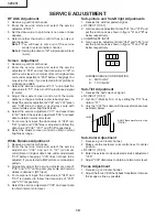
RF AGC Adjustment

1. Receive a good local channel.

2. Enter the service mode and select the service

adjustment "R01".

3. Set the data value to point where no noise or beat

appears.

4. Select another channel to confirm that no noise or

beat appears.
Note 1 :

You will have to come out of the service

mode to select another channel.

Note 2 :

Setting the data to "00" will produce a black

raster.

Screen  Adjustment

1. Receive a good local channel.

2. Enter the service mode and select the service

adjustment "V03" and set the data value to "00" to

set the color level to minimum. (Record original data

code under adjustment "V03" before changing) You

may skip this step, if you selected a B/W picture or

monoscope pattern.

3. Select the service adjustment "V11" and adjust the

data value to "01", this turn off the luminance signal

(Y-mute).

4. Adjust the master screen control until the raster

darkens to the point where raster is barely seen.

5. Adjust the service adjustments "V06" red, "V07" green

and "V08" blue to obtain a good grey scale with

normal whites at low brightness level.

6. Select the service adjustment "V11" and reset data

to "00". Select the service adjustment "V03" and reset

data to obtain normal color level.

7. For component input, the data value of "V46" red,

"V47" green and "V48" blue is adjusted to follow the

data value of "V06", "V07" and "V08" respectively.

8. Reset the master screen control to obtain normal

brightness range.

White Balance Adjustment

1. Receive a good local channel.

2. Enter the service mode and select the service

adjustment "V03" and set to "00" (minimum

color)(Record original data code under adjustment

"V03" before changing). "V03" does not have to be

adjusted, if you selected a B/W picture or monoscope

pattern.

3. Alternately adjust the service adjustment data of

"V09" and "V10" until a good grey scale with normal

whites is obtained. (RF Input)

4. For component input, the data value of "V49" and

"V50" is adjusted to follow the data value of "V09"

and "V10" respectively.

5. Select the service adjustment "V03" and reset data

to obtain normal color level.

Sub-picture and Sub-Bright Adjustments

1. Receive the window pattern signal.

• 

RF INPUT (TU51)

2. Get into service adjustment data "V01" and "V05" and

set the luminance as shown in figure "A" and "B" as

below respectively.

• 

COMPONENT INPUT

3. Get in service adjustment data "V42" and "V45" and

set the luminance as shown in figure "A" and "B" as

below respectively.

LUMINESCENCE CONFIRMATION

A:   92

±

10cd/m

2

B:   1.1

±

0.5cd/m

2

Sub-Tint Adjustment

1. Receive the half color bar signal.

• 

RF INPUT (TU51)

2. Get into Y-Mute by R/C, or by setting the "V11" bus

data to "01".

3. Vary the "V02" bus data until the waveform becomes

as stated below.

Sub-Color Adjustment

1. Receive a good local channel.

2. Make sure the customer  color control is set to center

position .

• 

RF INPUT (TU51)

3. Enter the service mode and select service adjustment

"V03".

4. Adjust "V03" data value to obtain a normal color level.

Focus Adjustment

1. Receive a good local channel.

2. Adjust the focus VR of the flyback transformer to make

the image as fine as possible.

A

B

B-AMP Base waveform in step
(TP47B)

LEVEL

Summary of Contents for 32C231

Page 1: ... DIAGRAMS 17 PRINTED WIRING BOARD ASSEMBLIES 26 REPLACEMENT PARTS LIST 30 PACKING OF THE SET 39 CONTENTS SPEAKER SIZE 12 x 6 cm oval 2 pcs VOICE COIL IMPEDANCE 16 ohm at 400 Hz ANTENNA INPUT IMPEDANCE VHF UHF 75 ohm Unbalanced TUNING RANGES VHF Channels 2 thru 13 UHF Channels 14 thru 69 CATV Channels 1 thru 125 EIA Channel Plan U S A POWER INPUT 120V AC 60 Hz POWER RATING 135W PICTURE SIZE 3073cm2...

Page 2: ...gh voltage with a meter to be certain that the high voltage does not exceed the specified value and that it is regulating correctly 5 Do not use a picture tube other than that specified or make unrecommended circuit modifications to the high voltage circuitry 6 When trouble shooting and taking test measurements on a receiver with excessive high voltage avoid being unnecessarily close to the receiv...

Page 3: ...ent covers or shields isolation resistor capacity networks mechanical insulators etc 3 To be sure that no shock hazard exists check for leakage current in the following manner Plug the AC cord directly into a 120 volt AC outlet Do not use an isolation transformer for this test Using two clip leads connect a 1 5k ohm 10 watt resistor paralleled by a 0 15µF capacitor in series with all exposed metal...

Page 4: ...VOLUME UP DOWN k Increases sound l Decreases sound Changes or selects the TV adjustments on On Screen Displey MENU Press Accesses MAIN MENU Press again Exits MAIN MENU Infrared Transmitter Window DISPLAY Press Displays receiving channel for 4 seconds Press again Removes display Temporarily displays receiving channel when in Closed Caption mode CHANNEL UP DOWN a Selects next higher channel s Select...

Page 5: ...f the horizontal oscillator does not stop in step 5 the circuit must be repaired before the set is returned to the customer HIGH VOLTAGE CHECK High voltage is not adjustable but must be checked to verify that the receiver is operating within safe and efficient design limitations as specified checks should be as follows 1 Connect an accurate high voltage meter between ground and anode of picture tu...

Page 6: ... in the video adjustment menu to ensure customer controls are in their proper reset position 2 Service number selection Once in the service mode press the Ch up or Ch down button on the remote controller or at the set The service adjustment number will vary in increments of one from V01 to P08 Select the item you wish to adjust 3 Data number selection Press the Vol up or Vol down button to adjust ...

Page 7: ...2 3Eh Component Input 3E V44 COLOR COMPONENT 0 127 00h 7Fh 72 48h Component Input 48 V45 BRIGHT COMPONENT 0 127 00h 7Fh 84 54h Component Input V46 R CUT OFF COMPONENT 64 255 40h FFh 64 40h Component Input V47 G CUT OFF COMPONENT 64 255 40h FFh 64 40h Component Input V48 B CUT OFF COMPONENT 64 255 40h FFh 64 40h Component Input V49 G R DRIVE COMPONENT 0 127 00h 7Fh 64 40h Component Input V50 B DRIV...

Page 8: ... Slice LEVEL 0 255 00h FFh 54 36h 12 EX7 RLY DELAY TIME 0 255 00h FFh 0 00h For the power control 00 EX8 ADG ON TIME 0 255 00h FFh 10 0Ah For the power control 0A SERVICE NUMBER DATA ADJUSTMENT ITEM INITIAL VALUE RANGE OP1 OPTION1 0 255 00h FFh 247 F7h B7 OP2 OPTION2 0 255 00h FFh 253 FDh 3C OP3 OPTION3 0 255 00h FFh 15 0Fh 0C B SPECIAL SETTING C OPTION SETTING INITIAL VALUE RANGE NOTE FIXED VALUE...

Page 9: ...uttons on the TV set at service mode for more than 2 seconds will automatically write the above initial values into IC2101 NOTES X IC2101 IC3001 CRT Holding down both the VOL up and CH up buttons on the TV set in the service mode for more than 2 seconds will automatically write the above initial values into IC2101 Then perform a complete adjustment Adjust items related to picture tube only Adjust ...

Page 10: ... Adjustment 1 Receive a good local channel 2 Enter the service mode and select the service adjustment V03 and set to 00 minimum color Record original data code under adjustment V03 before changing V03 does not have to be adjusted if you selected a B W picture or monoscope pattern 3 Alternately adjust the service adjustment data of V09 and V10 until a good grey scale with normal whites is obtained ...

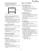
Page 11: ... select the service adjustment D08 for EW Trapezium 3 Adjust the D08 bus data to get the best position display DISPLAY OF TEXT BOX TEXT BOX A B A B 2 SPEC INSPECTION A B 2 5mm Ë MTS ADJUSTMENT MTS Level Adjustment 1 Set the sound volume above 1 Monoral signal 400Hz 100 modulation 2 Confirm EX4 data is 5Ah 3 Vary the M01 bus data until the voltage to pin 39 of IC3001 to become the value as stated b...

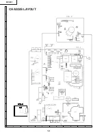
Page 12: ...12 32C231 6 5 4 3 2 1 A B C D E F G H CHASSIS LAYOUT ...

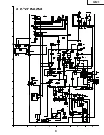
Page 13: ...13 32C231 6 5 4 3 2 1 A B C D E F G H BLOCK DIAGRAM ...

Page 14: ...14 32C231 ...

Page 15: ...32C231 15 ...

Page 16: ...32C231 16 ...

Page 17: ...32C231 17 ...

Page 18: ...18 32C231 ...

Page 19: ...32C231 19 ...

Page 20: ...32C231 20 ...

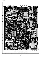
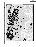
Page 21: ...21 32C231 6 5 4 3 2 1 A B C D E F G H PWB C 3 LINE Y C Unit Wiring Side PWB B CRT Unit Wiring Side PRINTED WIRING BOARD ASSEMBLIES PWB C 3 LINE Y C Unit Chip Parts Side ...

Page 22: ...22 32C231 6 5 4 3 2 1 A B C D E F G H PWB A MAIN Unit Wiring Side ...

Page 23: ...23 32C231 6 5 4 3 2 1 A B C D E F G H PWB A MAIN Unit Chip Parts Side ...

Page 24: ... TDA8177 AE IC602 VHiBA15218F2E X BA15218F E2 AB å IC701 VHiTEA1507 1 X TEA1507P N1 AE å IC702 RH FXA003WJZZ X PC123Y82 AB å IC703 VHiSE125N F X I C IC751 VHiPQ09RD11 1 X PQ09RD11 AD IC900 VHiCXA2089Q 2Y X CXA2089Q 6T AK IC1403 VHiPQ05RD11 1 X PQ05RD11 AD IC2001 RH iXA418WJZZQ X TMP88CS38BFG AN IC2040 VHiKiA7045A 1 X KIA7045AP AB IC2101 VHiBR2416E2 1 X BR24C16F AD IC3001 VHiCXA2074Q 1 X CXA2074Q A...

Page 25: ...K X 1000p 50V Ceramic AA C223 VCKYCY1CF104Z X 0 1 16V Ceramic AA C224 VCEA0A1HW474M X 0 47 50V Electrolytic AA C225 VCKYCY1CF104Z X 0 1 16V Ceramic AA C227 VCEA0A1HW106M X 10 50V Electrolytic AA C228 VCKYCY1CF104Z X 0 1 16V Ceramic AA C229 VCEA0A1CW477M X 470 16V Electrolytic AB C231 VCEA0A1EW476M X 47 25V Electrolytic AA C232 VCKYCY1HB222K X 2200p 50V Ceramic AA C233 VCEA0A1HW474M X 0 47 50V Elec...

Page 26: ...1HM104J X 0 1 50V Mylar AB C901 VCKYCY1HB103K X 0 01 50V Ceramic AA C902 VCKYCY1HB103K X 0 01 50V Ceramic AA C903 VCKYCY1HB681K X 680p 50V Ceramic AA C904 VCEA0A1HW105M X 1 50V Electrolytic AA C905 VCEA0A1HW105M X 1 50V Electrolytic AA C906 VCKYCY1HB681K X 680p 50V Ceramic AA C907 VCEA0A1HW105M X 1 50V Electrolytic AA C908 VCKYCY1HB103K X 0 01 50V Ceramic AA C909 VCEA0A1HW105M X 1 50V Electrolytic...

Page 27: ...de AA R422 VRS CY1JF000J X 0 1 16W Metal Oxide AA R430 VRS CY1JF391J X 390 1 16W Metal Oxide AA R431 VRS CY1JF331J X 330 1 16W Metal Oxide AA R432 VRS CY1JF102J X 1k 1 16W Metal Oxide AA R437 VRS CY1JF101J X 100 1 16W Metal Oxide AA R438 VRS CY1JF101J X 100 1 16W Metal Oxide AA R439 VRS CY1JF104J X 100k 1 16W Metal Oxide AA R436 VRS CY1JF000J X 0 1 16W Metal Oxide AA R441 VRS CY1JF472J X 4 7k 1 16...

Page 28: ... 100 1 16W Metal Oxide AA R938 VRS CY1JF223J X 22k 1 16W Metal Oxide AA R939 VRS CY1JF333J X 33k 1 16W Metal Oxide AA R940 VRS CY1JF8R2J X 8 2 1 16W Metal Oxide AA R941 VRS CY1JF101J X 100 1 16W Metal Oxide AA R942 VRS CY1JF223J X 22k 1 16W Metal Oxide AA R943 VRS CY1JF101J X 100 1 16W Metal Oxide AA R944 VRS CY1JF223J X 22k 1 16W Metal Oxide AA R945 VRS CY1JF101J X 100 1 16W Metal Oxide AA R946 V...

Page 29: ...1 4 AB P402 QPLGN0661CEZZA X Plug 6Pin CJ AB P601 QPLGN0161FJZZ X Plug 5Pin K1 5 AB P622 QPLGN0461CEZZA X Plug 4Pin YBN AB P651 QPLGN0361CEZZA X Plug 3Pin TP651 3 AB P702 QPLGN0269GEZZ X Plug 2Pin P1 2 AB P703 QPLGN0260CEZZ X Plug 2Pin M1 2 AB P2401 QPLGN0661CEZZA X Plug 6Pin AB RDA361 PRDAR0258PEFW X Heat Sink for IC361 AC RDA501 PRDARA039WJFW X Heat Sink for IC501 AD RDA601 PRDARA041WJFW X Heat ...

Page 30: ... VP XF100K0000 X Peaking 10µH AA L1404 VP XF220K0000 X Peaking 22µH AA L1405 VP XF220K0000 X Peaking 22µH AA L1408 VP XF100K0000 X Peaking 10µH AA CAPACITORS C1401 VCKYCY1HB103K X 0 01 50V Ceramic AA C1402 VCEA0A1AW227M X 220 10V Electrolytic AB C1403 VCCCCY1HH330J X 33p 50V Ceramic AA C1404 VCCCCY1HH181J X 180p 50V Ceramic AA C1405 VCKYCY1HB103K X 0 01 50V Ceramic AA C1406 VCKYCY1HB103K X 0 01 50...

Page 31: ...d AC QCNW B127WJZZ X Connecting Cord AB 1 CCABAA300WEH0 X Front Cabinet Ass y BH 1 1 Not Available Front Cabinet 1 2 GCOVAA398WJSA X RC LED Cover 1 3 HBDGB1009MESB X SHARP Badge AC 1 6 JBTN 0119GJKA X Button Power AB 1 7 JBTN A155WJKA X Button Menu CH Up Down VOL Up Down RRMCG1324CESC X Infrared R C Unit AH TiNS A708WJZZ X Operation Manual AD SPAKCA679WJZZ Packing Case SPAKP0110GJZZ Wrapping Paper...

Page 32: ... Case MARK Not replacement items FRONT Buffer Material Polyethylene Mat Polyethylene Bag Operation Manual Infrared R C unit Batteries REAR Use tape to fix the top side of packing case Use 12 staples to fix the bottom side of packing case ...

Page 33: ... means electronic mechanical photocopying recording or otherwise without prior written permission of the publisher SHARP ELECTRONICA MEXICO S A DE C V Quality Reliability Control Center Blvd SHARP No 3510 Parque Industrial Rosarito Playas de Rosarito México B C 22710 QRC0002 U April 2003 A J J B Design and Production Information Design base JAPAN Production SEMEX Modify SEMEX ...

Reviews: