
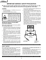


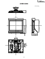


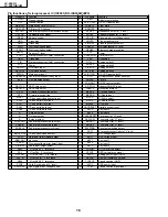
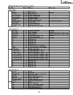

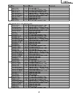


12
LC-20E1U
LC-20E1UB/UW
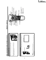
»
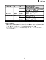
Precautions in handling the LCD panels
1. Work in a clean room (with humidities below 50%).
2. Be sure to wear an anti-static armband.
3. Handle the panels on an electroconductive mat.
4. Be careful not to fall, shake and shock the panels.
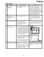
15. Remove the LCD panel unit fixing screws (4 pcs.).
16. Remove the ITO earth spring fixing screw (1 pc.).
17. Remove the reflection/deflection, prism, diffusion, ITO sheets and diffusion panel.
18. Remove the lamp fixing holder fixing screws (6 pcs.).
19. Detach the lamp unit-A/B.
20. Remove the reflection mirror fixing screws. (6 pcs.).
20
19
18
16
17
18
15
15
Back shield Panel
(PSLDM4685CEFW)
Reflection Mirror
(PMiR-0296CEZZ)
Lamp Fixing Holder
(LHLDZ2176CEZZ)
Diffusion Panel
(PCOVU0107CEZZ)
ITO Sheet
(PSHEP0289CEZZ)
Prism Sheet
(PSHEP0287CEZZ)
20" LCD Panel Unit
Reflection/Deflection Sheet
(PSHEP0286CEZZ)
Diffusion Sheet
(PSHEP0288CEZZ)
ITO Earth Spring
(MSPRP1220CEFW)
Lamp Fixing Holder
(LHLDZ2176CEZZ)
Lamp Unit-B
(KLMP-0125CEZZ)
Lamp Unit-A
(KLMP-0124CEZZ)
Summary of Contents for Aquos LC 20E1U
Page 32: ...35 34 LC 20E1U LC 20E1UB UW 12 11 10 9 8 7 6 5 4 3 2 1 A B C D E F G H OVERALL WIRING DIAGRAM ...
Page 35: ...39 38 LC 20E1U LC 20E1UB UW 12 11 10 9 8 7 6 5 4 3 2 1 A B C D E F G H Ë DIGITAL Unit 1 5 ...
Page 36: ...41 40 LC 20E1U LC 20E1UB UW 12 11 10 9 8 7 6 5 4 3 2 1 A B C D E F G H Ë DIGITAL Unit 2 5 ...
Page 37: ...43 42 LC 20E1U LC 20E1UB UW 12 11 10 9 8 7 6 5 4 3 2 1 A B C D E F G H Ë DIGITAL Unit 3 5 ...
Page 38: ...45 44 LC 20E1U LC 20E1UB UW 12 11 10 9 8 7 6 5 4 3 2 1 A B C D E F G H Ë DIGITAL Unit 4 5 ...
Page 39: ...47 46 LC 20E1U LC 20E1UB UW 12 11 10 9 8 7 6 5 4 3 2 1 A B C D E F G H Ë DIGITAL Unit 5 5 ...
Page 40: ...49 48 LC 20E1U LC 20E1UB UW 12 11 10 9 8 7 6 5 4 3 2 1 A B C D E F G H Ë ANALOG Unit 1 2 ...
Page 41: ...51 50 LC 20E1U LC 20E1UB UW 12 11 10 9 8 7 6 5 4 3 2 1 A B C D E F G H Ë ANALOG Unit 2 2 ...
Page 42: ...52 6 5 4 3 2 1 A B C D E F G H LC 20E1U LC 20E1UB UW Ë INVERTER A Unit ...
Page 43: ...53 6 5 4 3 2 1 A B C D E F G H LC 20E1U LC 20E1UB UW Ë INVERTER B Unit ...
Page 46: ...56 6 5 4 3 2 1 A B C D E F G H LC 20E1U LC 20E1UB UW DIGITAL Unit Side B ...
Page 49: ...59 6 5 4 3 2 1 A B C D E F G H LC 20E1U LC 20E1UB UW ANALOG Unit Side A ...
Page 51: ...62 6 5 4 3 2 1 A B C D E F G H LC 20E1U LC 20E1UB UW INVERTER A Unit Side A ...
Page 53: ...64 6 5 4 3 2 1 A B C D E F G H LC 20E1U LC 20E1UB UW INVERTER B Unit Side A ...


