background image

61

60

LC-20E1U
LC-20E1UB/UW

12

11

10

9

8

7

6

5

4

3

2

1

A

B

C

D

E

F

G

H

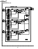
ANALOG Unit (Chip Parts Side-A)

P3704

R3755

R3753

R3758

R3208

C3205

C3210

R3207

J3500

R3550

P3504

R3530

C3511

R3551

R3532

R3558

R3531

R3411

R3410

R3413 C3401

C3513

Q3502

R3409

R3412

C3516

Q3501

Q3503

R3537

R3542

C3325

R3536

R3538

R3527

Q3505

R3540

R3339

R3336

L3500

C3515

R3337

C3519

C3324

C3742

R3340

R3335

R3338

C3743

R3401

D3401

R3402

R3754

C3392

Q3708

R3391

P3703

R3393

P3403

W2

R3394

R3392

C3393

SC3403

D3710

R3767

R3534

C3514

R3539

R3535

Q3504

R3533

C3512

R3353

R3354

C3384

R3372

C3383

R3384

C3358

R3357

C3357

C3356

C3355

P3702

C3354

C3380

C3352

C3351

FB3302

C3373

Q3202

R3356

L3301

R3206

C3348

C3346

R3204 C3204

R3434

C3347

R3368

C3353

Q3201

R3203

R3205

C3727

C3203 R3202

C3728

L3201

C3729

C3202

C3201

R3201

C3734

R3734

R3751

R3735

IC3702

R3736

C3733

Q3706

R3741

R3750

C3732 R3749 R3742

C3209

R3733

C3730

C3738

R3752

C3206

R3746 R3745 R3743

R3367

Q3205

Q3204

Q3203

R3762

Q3704

C3716

Q3710

C3701

R3710

D3711

R3705

R3703

C3702

R3759

C3704

R3704

Q3709

C3740

R3768

R3706

R3766

C3703

Q3702

C3700

Q3701

R3702

D3700

F3702-1

R3701

R3756

R3700

Q3700

W1

P3602

P3601

R3602

R3600

D3601

D3602

C3607

D3600

C3710

R3605

C3606

Q3602

C3603

C3605

R3609

R3604

R3608

R3607

C3602

C3604

C3601

R3601

Q3601

R3603

D3603

D3606

D3605

C3600

D3703

R3718

Q3603

R3606

D3607

D3604

Q3600

C3608

FB3701

FB3706

C3609

Q3604

C3711 C3713

D3608

R3721 R3720

R3722

FB3709

R3610

FB3700

R3717

FB3703

R3719

D3702

R3716

C3712

T3701

C3368

IC3701

C3367

C3714

R3707

C3706 R3708

C3365

C3705

C3364

FB3705

FB3707

R3711

FB3708

C3708

     3704

C3707

R3763

D3705

D3704

C3715

R3723

C3362

R3709

R3724

R3725

C3720

R3761

R3765

R3728

C3361

D3707

R3726

R3760

D3708

C3719 R3727

R3764

R3731

C3721

R3732

C3725

C3363

C3722

C3360

D3706

L3704

C3717

R3740

R3730

Q3707

R3739

R3738

C3737

C3386

C3724

C3718

L3703

R3729

C3735

R3345

C3741

C3304

C3305

R3310

D3709

R3737

R3302

R3314

R3324

R3320

C3312

R3318

R3317

C3314

R3323

C3310

C3374

R3376

C3375

R3371

R3375

C3504

C3505

C3350

C3349

L3303

C3339

R3507

R3512

R3513

C3342

C3345

C3344

C3343

C3341

C3390

C3391

C3340

C3333

C3319

R3330

R3511

R3510

R3506

R3325

C3503

R3332

C3526

C3322

C3317

R3500

C3501

R3328

R3509

C3338

R3547

IC3500

C3320

R3501

C3337

C3507

C3500

C3502

IC3304

R3505

R3508

C3517

C3336

C3334

C3525

R3369

C3506

R3504

R3546

IC3501

R3370

C3335

C3508

FB3301

R3385

C3330

C3382

R3523 C3518

L3302

Q3500

C3332

C3381

R3355

R3524 R3529 R3525

C3509

R3559

C3510

R3455

D3402

R3560

Q3513

R3557

R3555

R3556

R3554

C3520

D3502

R3526

D3501

R3528

R3553

R3552

C3321

R3341

R3331

R3329

C3323

C3318

R3334

R3562

R3344

C3522

C3316

R3326

IC3303

R3327

R3543

R3333

Q3512

C3315

R3544

R3377

Q3511

C3376

R3545

C3377 R3378 C3313

R3321

Q3510

R3315 C3311

R3322

IC3302

R3343

C3309

R3561 R3342

R3313

R3319

R3316

C3308

R3382

C3521

R3390

R3312

C3385

C3306

R3387

R3386

R3311

C3387

R3430 R3433

IC3301

R3309

R3306

R3346

R3429

R3432

R3304

C3301

R3303

R3388 R3399

C3389

C3303 C3302

R3389 C3388

R3305

R3428

R3431

R3307

R3308

C3329

C3366

C3359

R3362

R3352

R3350

R3351

R3360

R3379

D3301

Q3304

R3365

Q3306

R3380

R3361

R3381

C3328

R3373

R3358 R3383

R3363

Q3305

D3302

R3902

R3366

R3359

R3348

R3347

R3349

Q3303

R3364

C3370

R3374

P3503

R3757

R3901

P3500

P3502 P3501

Summary of Contents for Aquos LC 20E1U

Page 1: ...NUAL 6 DIMENSIONS 9 REMOVING OF MAJOR PARTS 10 ADJUSTING PROCEDURE OF EACH SECTION 14 TROUBLE SHOOTING TABLE 26 CHASSIS LAYOUT 30 BLOCK DIAGRAM 32 OVERALL WIRING DIAGRAM 34 DESCRIPTION OF SCHEMATIC DIAGRAM 36 SCHEMATIC DIAGRAM 37 PRINTED WIRING BOARD ASSEMBLIES 54 REPLACEMENT PARTS LIST 66 PACKING OF THE SET 79 Page SHARP CORPORATION This document has been published to be used for after sales serv...

Page 2: ... parts shown in this service manual may create shock fire or other hazards WARNING 1 For continued safety no modification of any circuit should be attempted 2 Disconnect AC power before servicing BEFORE RETURNING THE RECEIVER Fire Shock Hazard Before returning the receiver to the user perform the following safety checks 1 Inspect all lead dress to make certain that leads are not pinched and check ...

Page 3: ... manuel peut provoquer des électrocutions incendies radiations X ou autres accidents AVERTISSEMENT 1 N entreprendre aucune modification de tout circuit C est dangereux 2 Débrancher le récepteur avant toute réparation VERIFICATIONS CONTRE L INCEN DIE ET LE CHOC ELECTRIQUE Avant de rendre le récepteur à l utilisateur effectuer les vérifications suivantes 1 Inspecter tous les faisceaux de câbles pour...

Page 4: ...C which is higher than the conventional lead solder by 40 C and as it has poor solder wettabillty you may be apt to keep the soldering bit in contact with the PWB for extended period of time However Since the land may be peeled off or the maximum heat resistance temperature of parts may be excoeded remove the bit from the PWB as soon as you conurm the steady soldering condition Lead free solder co...

Page 5: ... Yes Brightness 430 cd m2 Lamp life 60 000 hours Viewing angles H 170 V 170 Audio amplifier 2 5 W 2 Speakers 1 37 64 2 3 4 in 4 7 cm 2 pcs AV1 AV IN1 S VIDEO IN AV2 AV IN2 AV OUT Terminals COMPONENT COMPONENT IN AUDIO IN Antenna F Type Headphone Mini jack for stereo ø 3 5 mm OSD language English French Spanish Power Environmental Conditions supply DC 0 C 40 C 13 V AC 110 240 V 50 60 Hz Weight 15 7...

Page 6: ...The screen cannot be set up straight When changing the angle make sure to hold the stand and adjust the screen to the best viewable angle POWER indicator A green indicator lights when the power is on and a red indicator lights when in the standby mode the indicator will not light when the main power is off Adjustable range AV IN 1 L R AUDIO S VID EO ANT VIDEO POWE R INPUT DC13V HEAD PHON E Y P B C...

Page 7: ...phones are not included in the supplied accessories No sound will be heard from the main unit speakers when a headphone mini plug is connected into the HEADPHONE jack On screen display 60 VOLUME Rear terminal AV IN 1 L R AUDIO S VIDE O ANT VIDEO POWER INPUT DC13V HEAD PHONE AV IN 1 L R AUDIO S VIDE O ANT VIDEO POWER INPUT DC12V HEAD PHONE Y P B COMPON ENT P R L L R AV IN 2 OUT VIDEO AUDIO R AUDIO ...

Page 8: ...deo terminal S VIDEO connection is recommended External devices that can be connected to AV IN1 terminal MENU SLEEP T IMER V I DEO ADJUST PRESET CLOSED CAPT I ON V CH I P BLOCK SET UP SELECT ENTER EX I T MENU SLEEP T IMER SELECT ADJUST EX I T MENU RETURN SLEEP T IMER REMA I N P I CTURE 30 T I NT COLOR BLACK LEVEL SHARPNESS SELECT ENTER EX I T MENU V I DEO ADJUST TV RETURN 0 0 0 0 BR I GHTNESS BR I...

Page 9: ...2 OUT COMPONENT L AUDIO R VIDEO S VIDEO L AUDIO R HEAD PHONE ANT POWER INPUT DC13V AV IN 1 POWER SLEEP CH VOL MENU MAIN POWER TV VIDEO 2 43 64 68 0 3 16 5 9 39 64 244 3 15 16 100 1913 32 493 2 1 64 51 5 315 16 100 17 21 64 440 75 32 182 243 64 68 7 23 64 187 8 27 64 214 43 64 103 ...

Page 10: ...ing screws 2 pcs 8 Remove the control PWB fixing screws 2 pcs 9 Detach the connector from each PWB 3 4 4 4 2 2 5 1 Cabinet A Cabinet B Stand Terminal Cover S Terminal Cover L Reinforcement Angle Inverter A PWB Inverter B PWB R C LED PWB Control PWB Analog PWB Digital Digital Digital PWB P6705 P6705 P3703 SC1201 SC1202 SC1202 SC1202 P4004 P4004 P4004 SC1203 SC1203 P2004 SC2001 SC2001 SC3403 SC3403 ...

Page 11: ...ews 1 pc 12 Remove the digital PWB fixing screws 3 pcs 13 Remove the analog PWB fixing screws 3 pcs and detatch the chassis frame cover fixing hooks 14 Remove the R C LED PWB fixing screws 2 pcs R C LED PWB 13 13 Chassis Frame Cover Chassis Frame Inverter A PWB Inverter B PWB Digital PWB Analog PWB 10 11 13 12 14 ...

Page 12: ... prism diffusion ITO sheets and diffusion panel 18 Remove the lamp fixing holder fixing screws 6 pcs 19 Detach the lamp unit A B 20 Remove the reflection mirror fixing screws 6 pcs 20 19 18 16 17 18 15 15 Back shield Panel PSLDM4685CEFW Reflection Mirror PMiR 0296CEZZ Lamp Fixing Holder LHLDZ2176CEZZ Diffusion Panel PCOVU0107CEZZ ITO Sheet PSHEP0289CEZZ Prism Sheet PSHEP0287CEZZ 20 LCD Panel Unit ...

Page 13: ... between Digita unit SC1202 and LCD panel unit and connect the extended cable QCNW A556WJZZ for service 5 Remove the FFC for connection between Digita unit SC1201 and LCD panel unit and connect the extended cable QCNW A555WJZZ for service 6 Remove the R C LED unit 6 1 Remove a lead from a wire holder 6 2 Remove the R C LED unit fixing screws 2 pcs 7 Remove the main unit fixing screws 3 pcs a subst...

Page 14: ... Short circuit TP2001 to GND and turn on the power Or short circuit TP2002 to GND and turn on the power Or holding down the TV VIDEO key and MENU key turn on the main power and simultaneously press the inspection process CH key and VOL key to change the mode to the adjustment mode Description The manual adjustment or adjustment through communication with the automatic machine is performed 3 Shippi...

Page 15: ...nd PAL N TAMP data 1 Receive the monoscope pattern sig nal 2 Adjust the RCUTOFF and BCUTOFF settings on page 2 of adjustment process mode to achieve an optimum white balance 1 Adjust the B Adj value to 5 0 0 02V with R3760 Make exact adjustment of the 5 00V level be cause it will be the reference for all the other supply voltages Be sure to make this adjustment together with the main PWB digital P...

Page 16: ... 0 Black Level 0 SHARPNESS 0 RED BLUE 0 GREEN 0 TV Color System N358 AV Color System N358 Language English Blue Screen Off EZ Setup Auto Start On Sleep Timer None MTS Stereo Brightness Bright Auto Power Off Off Picture Flip Normal AV2 IN OUT In CC TEXT OFF V Chip block MPAA None TV Guideline None Block Content All Unblock Status Off Input Secret No Clear ...

Page 17: ...n 2 1 Getting the test pattern displayed Put the screen in AV1 AV2 or COMPONENT but keep out any signal Call the adjustment process mode select G A TEST PATTERN in the 13th line of page 17 turn on the setting and the following test pattern shows up 2 2 Test pattern The following test pattern appears Note When the IC801 and IC1201 test pattern display commands are both turned on at the same time th...

Page 18: ...elect DAC2 chip select D terminal connection detect D terminal control line I2 C bus open closed select input I2 C bus serial clock line 2 I2 C bus serial clock line 1 I2 C bus serial data line 1 I2 C bus serial data line 2 R signal output G signal output B signal output Sub microprocessor data output Sub microprocessor data input Sub microprocessor clock input I2 C bus open closed output No signa...

Page 19: ...djustment TAMP H CA Y upper limit setting at TAMP adjustment TAMP L BB Y lower limit setting at TAMP adjustment GAIBU VER External version display 3 TV NTSC CONT 51 Video contrast setting TV NTSC TV PAL M CONT 51 Video contrast setting TV PAL M TV PAL N CONT 51 Video contrast setting TV PAL N AV N358 CONTRAST 49 Video contrast setting Composite S Video AV PAL CONTRAST 49 Video contrast setting Com...

Page 20: ...PAL BRIGHTNESS 68 Brightness setting component DVD PAL CONTRAST 26 Video setting component DVD PAL P FILTER 1 Peaking filter setting component DVD PAL H PEAKING 4 Picture quality setting component DVD PAL BRIGHT2 8 Brightness setting 2 component DVD PAL CONTRAST2 48 Video setting 2 component Video adjustments component 10 N358 TV COLOR 2500 Color density setting TV N358 AV COLOR 2500 Color density...

Page 21: ...phase setting TV PAL M AV LDLY 0 Y C phase setting composite S video 15 PAL N TV COLOR 2500 Color density setting TV PAL N AV COLOR 2500 Color density setting composite S video PAL N TV TINT 40 Color tone setting TV PAL N AV TINT 56 Color tone setting composite S video PAL N BRIGHTNESS 8 Brightness setting TV composite S video PAL N PEAKING FILTER 1 Peaking filter setting TV composite S video PAL ...

Page 22: ... phase NTSC 14 02 System clock setting G A TEST PATERN OFF Gradation test pattern display LCD controller IC test pattern 18 PAL 01 8E Initial settings PAL 02 C8 Various settings PAL 03 81 RCUTOFF PAL 04 00 GCUTOFF PAL 05 81 BCUTOFF PAL 06 14 Horizontal display position PAL 07 18 Vertical display position PAL 08 O2 UV data phase delay PAL 09 4C Panel clock adjustment PAL 0A 4A Display screen top bo...

Page 23: ...r reference voltage V0 BIAS 80 Gradation power reference voltage VGL ADJ 27 VGL bias setting VGL COM 215 VGL COM setting COM 179 COM amplitude setting G A READDATA 00 00 Controller read data setting G A READDATA WAIT Read execution Gradation COM settings 21 3D Y C 2 3D ON OFF setting 3D Y C DATA 0 3D YC data write read 3D Y C DATA WAIT Write read execution LSYNC 625 Sync ID threshold level TV HSYN...

Page 24: ...he Public mode Hold down the TV VIDEO and MENU buttons at once and press the MAIN POWER switch to power on the TV set Then press the CH and VOL buttons at once to go to the adjustment process mode Now press the MENU button and select PUBLIC MODE Press the VOL button to turn on the Public mode And power off the TV set 4 Making settings in the Public mode Before taking the steps below make sure the ...

Page 25: ...L START AV1 FIXED RESET ENTER Sets the highest sound volume level The volume level is expressed in digital form only Makes the sound volume adjustable Keeps the sound volume fixed The sound volume is fixed at the then level The Volume and Mute characters are not displayed onscreen Activates the remote controller Deactivates the remote controller The buttons on the TV set are operative Activates th...

Page 26: ... following points 1 Backlight lamp 2 Inverter circuit inverter PWB and main PWB F6700 F6701 F6702 F6703 F6704 D6700 D6701 Q6700 Q6701 Q6702 Q6703 Q6704 Q6705 Q6706 Q6707 Q6708 Q6709 Q6710 Q6711 Q6712 Q6713 Q6714 and their peripheral parts as well as pin 34 of IC1201 3 Lamp error detection circuit terminal PWB and main PWB D3600 D3601 D3602 D3603 D3604 D3605 D3606 D3607 D3608 Q3600 Q3601 Q3602 Q360...

Page 27: ...001 as specified Check IC7202 and its peripheral parts Yes No Are input and output of IC7202 as specified No Are pin 67 of IC2001 at H No S VIDEO output Yes Yes Are pins 2 and 12 of IC7101 60th at H No Are inputs at Pins 71 and 72 of IC801 as specified Check SC3405 SY line SC line and peripheral parts No COMPONENT output No Is input at Pins 4 5 6 and 75 of IC801 as specified Check J3404 DVD Y line...

Page 28: ...econdary side load of T3701 Fluorescent lamp Yes No Does F6700 F6701 F6702 F6703 and F6704 function Yes No Is Pin 34 of IC1201 at H Yes No Are the oscillation waveforms at the primary side of T6700 T6702 T6704 T6706 and T6708 as specified Yes Replace F6700 F6701 F6702 F6703 and F6704 No Is input at Pin 71 of IC801 as specified Check SC3405 SC line and peripheral parts Yes Check the line IC1201 and...

Page 29: ...eck the line in question IC3301 and its peripheral parts Yes Check the speakers and their peripheral parts No sound from headphone Yes No Is pin 55 of IC2001 at L Check the headphone and its peripheral parts Check Q2007 J3500 harness and their peripheral parts No sound from output line Yes No Is pin 58 of IC2001 at L No Are outputs at pins 14 and 15 of IC3501 as specified Yes Check the line in que...

Page 30: ...31 30 LC 20E1U LC 20E1UB UW 12 11 10 9 8 7 6 5 4 3 2 1 A B C D E F G H CHASSIS LAYOUT ANALOG Unit CONTROL Unit DIGITAL Unit R C LED Unit INVBERTER A Unit INVBERTER B Unit ...

Page 31: ...1112 IC1114 IC1115 DAC IC1101 IC1111 COMMON IC1113 IC1109 Q1101 Q1102 Q1108 Q1109 I2C 3 WIRE CK VD HD OSD RGB V1 SY SC DIGITAL UNIT V1SY V1SC AUDIO IN OUT SWITCH IC3501 Q3500 CONTROL KEYS POWER SWITCH CONTROL UNIT DC DC T3701 IC3701 Q3700 Q3701 Q3702 38V 9V 5V 8V 20V REGULATOR IC3702 31V Q3707 29V Q3704 8V Q3706 R C RECEIVER RMC4002 RC LED UNIT LED D4014 D4015 VIDEO IN OUT SWITCH Q3501 Q3505 BUS S...

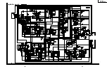
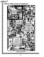
Page 32: ...35 34 LC 20E1U LC 20E1UB UW 12 11 10 9 8 7 6 5 4 3 2 1 A B C D E F G H OVERALL WIRING DIAGRAM ...

Page 33: ...ng CAPACITOR 1 All capacitors are µF unless otherwise noted P pF µµF 2 All capacitors are 50V unless otherwise noted 3 All capacitors are Ceramic type unless otherwise noted ML Mylar TA Tantalum PF Polypro Film ST Styrol CAUTION This circuit diagram is original one therefore there may be a slight difference from yours IMPORTANT SAFETY NOTICE PARTS MARKED WITH å A R E IMPORTANT FOR MAINTAINING THE ...

Page 34: ...37 6 5 4 3 2 1 A B C D E F G H LC 20E1U LC 20E1UB UW SCHEMATIC DIAGRAM ËR C LED and CONTROL Unit R C LED ...

Page 35: ...39 38 LC 20E1U LC 20E1UB UW 12 11 10 9 8 7 6 5 4 3 2 1 A B C D E F G H Ë DIGITAL Unit 1 5 ...

Page 36: ...41 40 LC 20E1U LC 20E1UB UW 12 11 10 9 8 7 6 5 4 3 2 1 A B C D E F G H Ë DIGITAL Unit 2 5 ...

Page 37: ...43 42 LC 20E1U LC 20E1UB UW 12 11 10 9 8 7 6 5 4 3 2 1 A B C D E F G H Ë DIGITAL Unit 3 5 ...

Page 38: ...45 44 LC 20E1U LC 20E1UB UW 12 11 10 9 8 7 6 5 4 3 2 1 A B C D E F G H Ë DIGITAL Unit 4 5 ...

Page 39: ...47 46 LC 20E1U LC 20E1UB UW 12 11 10 9 8 7 6 5 4 3 2 1 A B C D E F G H Ë DIGITAL Unit 5 5 ...

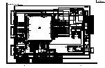
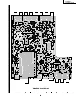
Page 40: ...49 48 LC 20E1U LC 20E1UB UW 12 11 10 9 8 7 6 5 4 3 2 1 A B C D E F G H Ë ANALOG Unit 1 2 ...

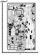
Page 41: ...51 50 LC 20E1U LC 20E1UB UW 12 11 10 9 8 7 6 5 4 3 2 1 A B C D E F G H Ë ANALOG Unit 2 2 ...

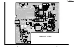
Page 42: ...52 6 5 4 3 2 1 A B C D E F G H LC 20E1U LC 20E1UB UW Ë INVERTER A Unit ...

Page 43: ...53 6 5 4 3 2 1 A B C D E F G H LC 20E1U LC 20E1UB UW Ë INVERTER B Unit ...

Page 44: ...54 6 5 4 3 2 1 A B C D E F G H LC 20E1U LC 20E1UB UW PRINTED WIRING BOARD ASSEMBLIES DIGITAL Unit Side A ...

Page 45: ...172 R1170 R1001 C1149 D1108 Q1103 R1010 R1169 R1029 R7019 R7020 C7033 R7030 R7022 C7029 FL7002 C7030 R7016 R7021 C7027 FL7001 C7113 R7012 R7112 C7031 FL7003 C7015 C7036 C7053 R7051 R7052 C7046 R7025 C7701 D7701 C7054 C7047 C7048 FB7004 FB7003 FL7004 C2020 R422 C7122 C7205 C7204 R7203 R417 IC7201 L401 C412 C413 Q403 C7203 R425 C411 R416 R414 IC7202 R7204 C7201 R423 C7202 FL401 R424 R7201 R7202 C410...

Page 46: ...56 6 5 4 3 2 1 A B C D E F G H LC 20E1U LC 20E1UB UW DIGITAL Unit Side B ...

Page 47: ...002 C1145 R1155 R1156 R1026 IC1116 R1025 R1134 R1033 IC1101 R1228 R1031 IC702 D1201 Q1109 Q1108 C1153 C1116 R1145 C705 R1120 D1101 D1107 R1122 R1023 C2008 R1130 R1022 Q1106 R1020 C1151 R1021 R919 R908 R904 R907 C905 R909 R902 R906 IC903 R835 C804 X801 C802 R803 R802 R801 C806 C805 TP802 TP801 R810 IC801 R813 C822 C827 C830 R804 C837 C831 R819 C808 C825 C828 C824 C836 C832 R814 FB802 C823 C807 C811...

Page 48: ...Chip Parts Side A P4005 D4013 D4012 D4022 R4021 C4018 R4029 R4024 D4014 Q4003 Q4007 R4023 R4030 R4031 D4015 R4032 Q4004 SW4008 SW4007 R4006 R4005 SW4002 SW4003 R4011 R4012 SW4004 SW4006 D4008 D4009 D4010 P4004 CONTROL Unit Side A QPWBSB413WJZZ CONTROL Unit Chip Parts Side A QPWBSB413WJZZ ...

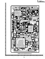
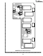
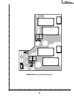
Page 49: ...59 6 5 4 3 2 1 A B C D E F G H LC 20E1U LC 20E1UB UW ANALOG Unit Side A ...

Page 50: ...14 R3707 C3706 R3708 C3365 C3705 C3364 FB3705 FB3707 R3711 FB3708 C3708 3704 C3707 R3763 D3705 D3704 C3715 R3723 C3362 R3709 R3724 R3725 C3720 R3761 R3765 R3728 C3361 D3707 R3726 R3760 D3708 C3719 R3727 R3764 R3731 C3721 R3732 C3725 C3363 C3722 C3360 D3706 L3704 C3717 R3740 R3730 Q3707 R3739 R3738 C3737 C3386 C3724 C3718 L3703 R3729 C3735 R3345 C3741 C3304 C3305 R3310 D3709 R3737 R3302 R3314 R3324...

Page 51: ...62 6 5 4 3 2 1 A B C D E F G H LC 20E1U LC 20E1UB UW INVERTER A Unit Side A ...

Page 52: ...nit Chip Parts Side A C6712 R6708 Q6706 R6710 C6713 Q6708 R6709 Q6707 R6711 R6722 D6700 P6705 Q6704 R6721 R6720 R6705 R6707 R6706 C6708 Q6705 Q6703 C6707 R6704 T6700 T6701 P6700 C6702 Q6700 R6700 Q6701 Q6702 R6701 C6703 R6702 R6703 T6702 P6701 T6703 T6704 P6702 T6705 ...

Page 53: ...64 6 5 4 3 2 1 A B C D E F G H LC 20E1U LC 20E1UB UW INVERTER B Unit Side A ...

Page 54: ... G H LC 20E1U LC 20E1UB UW INVERTER B Unit Chip Parts Side A Q6712 Q6713 R6716 R6717 C6722 R6719 R6718 C6723 Q6714 Q6709 Q6710 R6712 R6713 C6717 R6724 R6723 Q6711 D6701 C6718 P6706 R6715 R6714 T6706 T6707 P6703 T6708 T6709 P6704 ...

Page 55: ... DU MODELE 2 NO DE REF 3 NO DE PIECE 4 DESCRIPTION in CANADA Contact SHARP Electronics of Canada Limited Phone 416 890 2100 MARQUE SECTION LIVRAISON DES PIECES DE RECHANGE DUNTKA670FE29 DIGITAL UNIT PRINTED WIRING BOARD ASSEMBLIES NOT REPLACEMENT ITEM DUNTKA670FE29 DIGITAL Unit DUNTKB412DE03 ANALOG Unit DUNTKB413DE03 CONTROL Unit DUNTKB414DE03 R C LED Unit DUNTKB416DE01 INVERTER A Unit DUNTKB417DE...

Page 56: ...µH AB L1205 VP 1M220J2R9NY J Peaking 22µH AB L7001 VP 1M4R7J1R2NY J Peaking 4 7µH AB L7002 VP 1M220J2R9NY J Peaking 22µH AB L7003 VP 1M220J2R9NY J Peaking 22µH AB CAPACITORS C401 VCKYTV1AB105K J 1 10V Ceramic AD C401 VCKYTV1AB105KY J 1 10V Ceramic AC C402 VCKYCY1HB102KY J 1000p 50V Ceramic AA C403 VCKYCY1EF104ZY J 0 1 25V Ceramic AA C404 VCEAPF0JW476MY J 47 6 3V Electrolytic AB C405 VCKYCY1HB222KY...

Page 57: ...04ZY J 0 1 50V Ceramic AB C2001 VCKYCY1HB102KY J 1000p 50V Ceramic AA C2002 VCCCCY1HH221JY J 220p 50V Ceramic AA C2003 VCKYTV1AB105KY J 1 10V Ceramic AC C2007 VCKYCY1EF104ZY J 0 1 25V Ceramic AA C2009 VCKYCY1EF104ZY J 0 1 25V Ceramic AA C2010 VCKYCY1EF104ZY J 0 1 25V Ceramic AA C2015 VCKYCY1HB561KY J 560p 50V Ceramic AA C2016 VCKYCY1EF104ZY J 0 1 25V Ceramic AA C2017 VCKYCY1EF104ZY J 0 1 25V Ceram...

Page 58: ...Y J 47k 1 16W Metal Oxide AA R1020 VRS CY1JF472JY J 4 7k 1 16W Metal Oxide AA R1021 VRS TW2ED102JY J 1k 1 4W Metal Oxide AA R1022 VRS CY1JF000JY J 0 1 16W Metal Oxide AA R1024 VRS CY1JF123FY J 12k 1 16W Metal Oxide AA R1025 VRS CY1JF123FY J 12k 1 16W Metal Oxide AA R1026 VRS CY1JF123FY J 12k 1 16W Metal Oxide AA R1027 VRS CY1JF123FY J 12k 1 16W Metal Oxide AA R1028 VRS CY1JF123FY J 12k 1 16W Metal...

Page 59: ...e AA R2022 VRS CA1JF101JY J 100 1 16W Metal Oxide AA R2029 VRS CY1JF223JY J 22k 1 16W Metal Oxide AA R2030 VRS CA1JF333JY J 33k 1 16W Metal Oxide AA R2033 VRS CB1JF101JY J 100 1 16W Metal Oxide AA R2041 VRS CY1JF101JY J 100 1 16W Metal Oxide AA R2042 VRS CY1JF101JY J 100 1 16W Metal Oxide AA R2043 VRS CB1JF101JY J 100 1 16W Metal Oxide AA R2044 VRS CY1JF103JY J 10k 1 16W Metal Oxide AA R2045 VRS C...

Page 60: ...M2147M 1Y J NJM2147M TE1 AF TRANSISTORS Q3201 VS2SC3928AR 1Y J 2SC3928AR AB Q3202 VS2SC3928AR 1Y J 2SC3928AR AB Q3303 VSDTA144EE 1Y J DTA144EE AA Q3304 VSDTC314TK 1Y J DTC314TK AC Q3305 VSDTC314TK 1Y J DTC314TK AC Q3306 VS2SC3928AR 1Y J 2SC3928AR AB Q3500 VSUMG4N 1Y J UMG4N AB Q3501 VS2SK1467 1Y J 2SK1467 AE Q3502 VS2SK1467 1Y J 2SK1467 AE Q3503 VS2SC3928AR 1Y J 2SC3928AR AB Q3504 VS2SC3928AR 1Y J...

Page 61: ...3368 VCEAPF1CN106MY J 10 16V Electrolytic AD C3369 RC EZ1274CEZZ J 1000 16V Electrolytic AD C3370 VCKYTV1CF105ZY J 1 16V Ceramic AB C3371 VCEA4A1CN228M J 2200 16V Electrolytic AF C3372 RC EZ1274CEZZ J 1000 16V Electrolytic AD C3375 VCKYCY1CB273KY J 0 027 16V Ceramic AB C3377 VCKYCY1CB273KY J 0 027 16V Ceramic AB C3380 VCKYCY1EF104ZY J 0 1 25V Ceramic AA C3382 VCKYCY1HB102KY J 1000p 50V Ceramic AA ...

Page 62: ...75 1 16W Metal Oxide AA R3431 VRS CY1JF000JY J 0 1 16W Metal Oxide AA R3432 VRS CY1JF000JY J 0 1 16W Metal Oxide AA R3433 VRS CY1JF000JY J 0 1 16W Metal Oxide AA R3434 VRS CY1JF103JY J 10k 1 16W Metal Oxide AA R3523 VRS CY1JF103JY J 10k 1 16W Metal Oxide AA R3524 VRS CY1JF103JY J 10k 1 16W Metal Oxide AA R3528 VRS CY1JF471JY J 470 1 16W Metal Oxide AA R3529 VRS CY1JF471JY J 470 1 16W Metal Oxide A...

Page 63: ...EZZY J Ferrite Bead AD J3301 QJAKF0066CEZZ J AUDIO L R COMPONENT AE J3401 QJAKG0085CEZZ J Y PB PR COMPONENT AG J3404 QJAKG0069CEZZ J AV IN AV IN2 OUT AG J3407 QJAKG0068CEZZ J Jack AV IN1 AG J3500 QJAKJ0046CEZZ J HEADPHONE AE J3701 QJAKE0193CEZZ J POWER INPUT DC 13V AK P3502 QPLGN0478GEZZ J Plug 4 pin AB P3601 QPLGN0478GEZZ J Plug 4 pin AB P3602 QPLGN0678GEZZ J Plug 6 pin AB P3702 QCNW A696WJZZ J P...

Page 64: ...0806CEZZQ J Transformer AM å T6705 RTRNZ0806CEZZQ J Transformer AM CAPACITORS C6702 VCKYCY1CB333KY J 0 033 16V Ceramic AA C6703 VCKYCY1CB333KY J 0 033 16V Ceramic AA C6704 VCEA4A1CN108M J 1000 16V Electrolytic AD C6707 VCKYCY1CB333KY J 0 033 16V Ceramic AA C6708 VCKYCY1CB333KY J 0 033 16V Ceramic AA C6709 VCEA4A1CN108M J 1000 16V Electrolytic AD C6712 VCKYCY1CB333KY J 0 033 16V Ceramic AA C6713 VC...

Page 65: ...CABAA072WJ03 J Cabinet A Ass y BL LC 20E1UW 1 1 Not Available Cabinet A 1 2 GCOVA2020CEZZ J R C LED Cover AF 1 3 Not Available SHARP Badge 1 4 PSPAGA027WJZZ J Spacer x2 AC 1 5 PSPAGA028WJZZ J Spacer x2 AB 1 6 PSPAGA029WJZZ J Spacer x2 AB 1 7 PSPAGA030WJZZ J Spacer x4 AB 1 8 PSPAHA040WJZZ J Spacer x2 AD 1 9 PSPAHA041WJZZ J Spacer x2 AD 1 10 PSPAH0678CEZZ J Spacer x2 AA 1 11 QCNW A543WJZZ Connecting...

Page 66: ... 7 5 2 5 20 5 20 5 10 5 4 5 5 5 6 5 7 5 8 5 9 5 1 5 19 5 21 5 14 5 15 5 13 5 12 5 17 5 16 5 18 5 19 5 19 5 7 5 19 13 5 11 C Inverter B PWB Inverter A PWB Digital PWB Analog PWB 1 13 1 12 1 9 1 6 1 6 1 6 1 4 1 8 1 7 1 7 K D G 1 13 1 11 1 2 1 3 1 12 1 4 1 8 1 6 1 5 1 1 22 11 1 H L L K 4 22 22 4 2 4 1 4 5 4 6 4 7 4 3 4 4 4 8 1 5 1 6 1 6 1 10 Control PWB R C LED PWB 1 7 1 7 3 3 3 6 3 5 3 3 4 3 2 3 1 ...

Page 67: ...al No Label LC 20E1U AE 15 TLABNA126WJZZ J Serial No Label AD LC 20E1UB 15 TLABNA127WJZZ J Serial No Label AD LC 20E1UW 16 LX BZ3442CEFF J Screw x4 AB LC 20E1U UB 16 LX BZ3442CEFN J Screw x4 LC 20E1UW AB 17 QCNW A267WJZZ J Connecting Cord AK 18 XBBSD40P06000 J Screw x4 AA 19 XBBSF30P06000 J Screw x2 AA 20 XBPSD30P10JS0 J Screw x8 AA 21 XEBSD30P08000 J Screw x1 AA 22 XEBSD30P12000 J Screw x6 AA 23 ...

Page 68: ...SPAKFA014WJZZ Wrapping Paper SPAKPA077WJZZ Buffer Material Partition SPAKFA093WJZZ AC Adapter UADP 0243CEPZ No Label TLABK0001TAZZ Packing Case SPAKCA128WJZZ LC 20E1U SPAKCA252WJZZ LC 20E1UB SPAKCA253WJZZ LC 20E1UW Buffer Material Bottom SPAKXA036WJZZ AC Cord QACCD3097CEPA Antenna Cable QCNWG0003CEPA Infrared R C Unit RRMCGA077WJSA LC 20E1U RRMCGA077WJSB LC 20E1UB RRMCGA077WJSC LC 20E1UW Not Repla...

Page 69: ...d in a retrieval system or transmitted in any form or by any means electronic mechanical photocopying recording or otherwise without prior written permission of the publisher SHARP CORPORATION AV Systems Group Quality Reliability Control Center Yaita Tochigi 329 2193 Japan D Japan P Japan TQ1390 S Sep 2002 Printed in Japan MI KG ...

Reviews: