background image

LC-42D72U

3 – 12

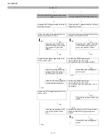
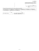
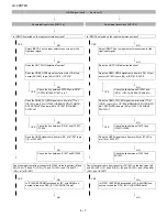
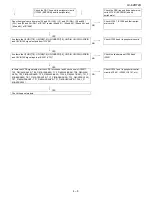
8. Adjustment of white balance

8.1. White balance adjustment

Adjustment item

Adjustment conditions

Adjustment procedure

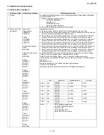
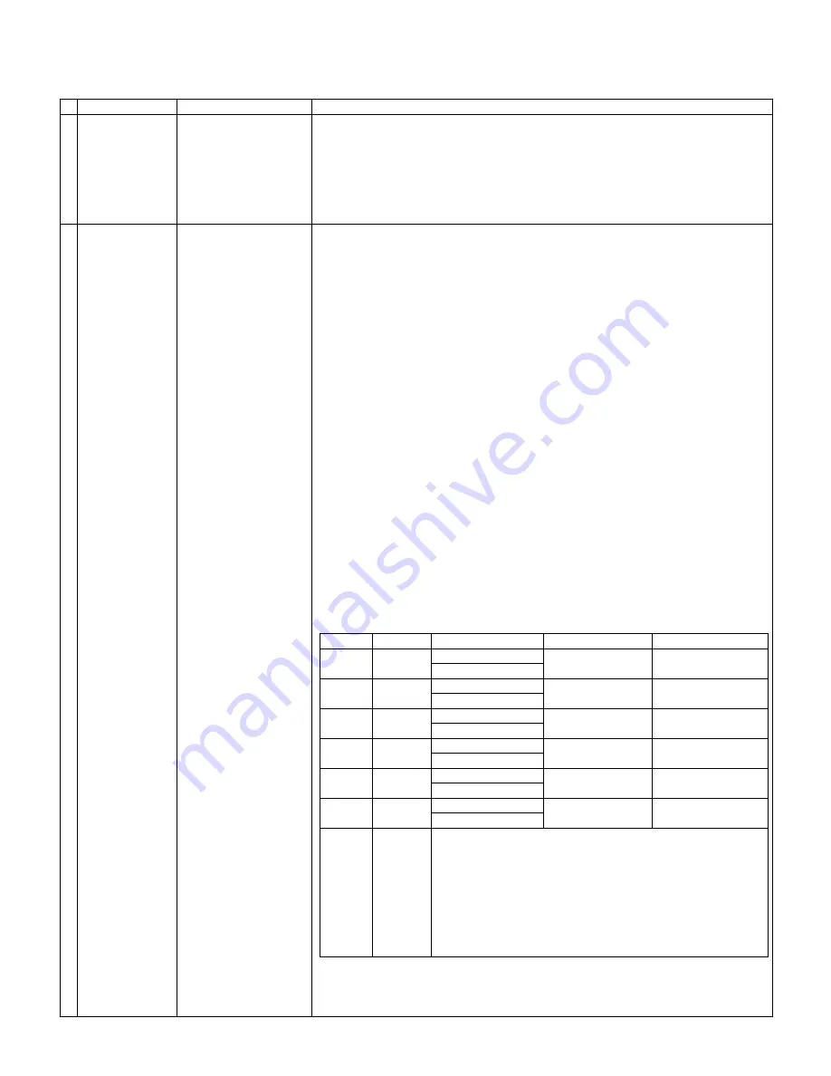
1 Setting

For detailed adjustment procedure, refer to ”Kameyama Model Integral Monitor WB Adjust-
ment Specifications V1.6”.
1) Make the following settings for the set.

             AV MODE: [DYNAMIC]
             Backlight: +16
             Active Backlight: OFF
             Aging Time: Min. 60 minutes

2) Connect the white balance adjustment tool to the set.

2 Execution of auto 

adjustment

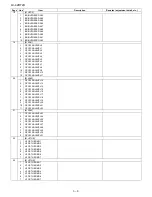
[Command]
Process mode
KRSW0001
KKT10037

Setting
KYOF0000
OSDS0001
SBSL0016

Multi-point adjustment 
mode
MSET0001 

Adjustment value initial-
ization
MSET0004 

Point 6
WBI60928
MG6G****
MG6B****
MG6R****

Point 5
WBI50800
MG5G****
MG5B****
MG5R****

[Adjustment procedure]
1) Using the remote controller, transmit the “monitor adjustment process” code.
2) Set the 6th point to the specified gradation level. With the strongest color being fixed, turn 

down the R, G and B settings to their reference levels.

3) Set the 5th point to the specified gradation level. Correct the G setting (800 x 6thpoint G 

setting / 928) (rounded off), and make the R and B settings to their reference levels.

4) Set the 4th point to the specified gradation level. Correct the G setting (656 x 6thpoint G 

setting / 928) (rounded off), and make the R and B settings to their reference levels.

5) Set the 3rd point to the specified gradation level. Correct the G setting (528 x 6thpoint G 

setting / 928) (rounded off), and make the R and B settings to their reference levels.

6) Set the 2nd point to the specified gradation level. Correct the G setting (352 x 6thpoint G 

setting / 928) (rounded off), and make the R and B settings to their reference levels.

7) Set the 1st point to the specified gradation level. Correct the G setting (184 x 6thpoint G 

setting / 928) (rounded off), and make the R and B settings to their reference levels.

8) With the MSET0003 command, write the adjustment values and turn off the AC power.
* Initial R, G and B settings at point 6: Gradation level set at 928
* Initial R, G and B settings at points 1 thru 5: Corrected G setting at each point
(This is because the adjustment is made to achieve the same remainder of RGB setting/4 at 
each point.)
[Adjustment values]

As per the “standard set” submitted by Engineering Department 

“LC-42D72U” Teaching set 
[Adjustment reference] Instrument: Minolta CA-210 Engineering instrument

Point 4

Level

Reference

Adjustment spec

Ins. spec

WBI40656

Point 6

928

X=0.272

±

0.0025

±

0.003

MG4G****

y=0.277

MG4B****

Point 5

800

X=0.272

±

0.0025

±

0.003

MG4R****

y=0.277

Point 4

656

X=0.272

±

0.0025

±

0.003

Point 3

y=0.277

WBI30528

Point 3

528

X=0.272

±

0.0035

±

0.0005

MG3G****

y=0.277

MG3B****

Point 2

352

X=0.272

±

0.0060

±

0.0010

MG3R****

y=0.277

Point 1

184

X=0.272

±

0.0100

±

0.0015

Point 2

y=0.277

WBI20352
MG2G****
MG2B****
MG2R****

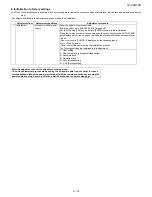
Note

Set conditions for inspection
AV MODE: [DYNAMIC] (Reset)
Monochro: ON
Active Backlight: OFF
Aging Time: Min. 60 minutes

Point 1
WBI10184
MG1G****
MG1B****
MG1R****

Writing
MSET0003

Summary of Contents for Aquos LC-42D72U

Page 1: ...MAJOR IC INFORMATIONS 5 1 CHAPTER 6 OVERALL WIRING DIAGRAM BLOCK DIAGRAM 1 OVERALL WIRING DIAGRAM 6 1 2 SYSTEM BLOCK DIAGRAM 6 3 3 MAIN BLOCK DIAGRAM 6 5 CHAPTER 7 PRINTED WIRING BOARD 1 R C LED UNIT PRINTED WIRING BOARD 7 1 2 KEY UNIT PRINTED WIRING BOARD 7 2 3 MAIN UNIT PRINTED WIRING BOARD 7 3 4 TERMINAL UNIT PRINTED WIRING BOARD 7 11 CHAPTER 8 SCHEMATIC DIAGRAM 1 DESCRIPTION OF SCHEMATIC DIA G...

Page 2: ...resistor All checks must be repeated with the AC cord plug connection reversed If necessary a nonpolarized adaptor plug must be used only for the purpose of completing these checks Any reading of 0 75 Vrms this corresponds to 0 5 mA rms AC or more is excessive and indicates a potential shock hazard which must be corrected before returning the monitor to the owner SAFETY NOTICE Many electrical and ...

Page 3: ...seaux de résistancecapacité les isolateurs mécaniques etc S assurer qu il n y ait pas de danger d électrocution en vérifiant la fuite de courant de la facon suivante Brancher le cordon d alimentation directem ent à une prise de cou rant de 120V Ne pas utiliser de transformateur d isolation pour cet essai A l aide de deux fils à pinces brancher une résistance de 1 5 kΩ 10 watts en parallèle avec un...

Page 4: ...solder by 40 C and as it has poor solder wettability you may be apt to keep the soldering bit in contact with the PWB for extended period of time However Since the land may be peeled off or the maximum heat resistance temperature of parts may be exceeded remove the bit from the PWB as soon as you confirm the steady soldering condition Lead free solder contains more tin and the end of the soldering...

Page 5: ...LC 42D72U 1 1 LC 42D72U Service Manual CHAPTER 1 OPERATION MANUAL 1 SPECIFICATIONS ...

Page 6: ...LC 42D72U 1 2 2 OPERATION MANUAL ...

Page 7: ...LC 42D72U 1 3 ...

Page 8: ...LC 42D72U 1 4 ...

Page 9: ...LC 42D72U 1 5 ...

Page 10: ...LC 42D72U 1 6 ...

Page 11: ...LC 42D72U 1 7 ...

Page 12: ...LC 42D72U 1 8 3 DIMENSIONS ...

Page 13: ...R 2 REMOVING OF MAJOR PARTS 1 REMOVING OF MAJOR PARTS 1 Remove the SD Card Cover 2 Remove the 4 lock screws and detach the Stand Base Ass y 3 Remove the 12 lock screws 5 lock screws and detach the Rear Cabinet 3 3 2 Stand Base Ass y Rear Cabinet 1 ...

Page 14: ...ck screws and detach the Stand Assist Angle 7 Remove the 2 lock screws and detach the Stand Assist Cover 8 Remove the 4 lock screws and detach the Stand Fixing Angle 9 Remove the 7 lock screws and detach the MAIN Shield 9 5 5 8 6 4 4 7 Center Angle L MAIN Shield Center Angle R Stand Fixing Angle Chassis Fixing Angle Stand Assist Cover Stand Assist Angle ...

Page 15: ...tors from all the PWBs 11 Remove the Top Cover Ass y Remove the 1 lock screw from the Top Cover Ass y and detach the KEY Unit 䬌䎮䎰䬍 䬌䎵䎤䬍 䬌䎳䎧䬍 䬌䎰䎤䬍 䬌䎵䎤䬍 䬌䎯䎹䬍 䬌䎮䎰䬍 䬌䎩䎦䬍䬌䎶䎤䬍 䬌䎳䎫䬍 䬌䎯䎥䬍 䬌䎯䎳䬍 䬌䎯䎹䬍 䬌䎳䎧䬍 䬌䎳䎫䬍 䬌䎶䎳䬍 䬌䎯䎤䬍 䬌䎯䎳䬍 䬌䎯䎤䬍 䬌䎯䎥䬍 11 Top Cover Ass y ...

Page 16: ... 4 lock screws and detach the TERMINAL Unit 16 Remove the 3 lock screws 2 lock screws and 3 rivet and detach the MAIN PWB Radiator and Earth plate and MAIN Unit 17 Remove the 2 lock screws and detach the Speaker L R 18 Remove the 2 lock screws and detach the R C LED Unit 16 16 16 16 14 12 13 13 13 13 15 17 17 18 Speaker R TERMINAL Unit Tray Chassis POWER Unit MAIN Unit MAIN PWB Radiator Terminal A...

Page 17: ...ngle top L R 20 Remove the 3 lock screws and detach the Lug Angle Top Center 21 Remove the 9 lock screws and detach the Lug Angle Bottom 22 Remove the LCD Panel Module 19 19 19 19 20 20 Lug Angle Top R Lug Angle Top Center Lug Angle Bottom Lug Angle Top L 21 21 21 ...

Page 18: ...r software The main software and the monitor microprocessor software can be upgraded by using a general purpose SD memory card The followings are the procedures for upgrading explained separately for each of the main software the monitor microprocessor software 2 2 Main software version upgrade 2 2 1 Get ready before you start SD memory card of 32MB or higher capacity PC running on Windows 98 98SE...

Page 19: ...ard drive do not store other folders or unrelated files or more than one binary image files for version upgrade Now the SD card for version upgrade is ready 2 2 3 Upgrading the software 1 Turn off the AC power Unplug the AC power cord 2 Insert the upgrading SD card prepared as instructed above into the service slot NOTE Be careful not to insert the SD card in the wrong way Otherwise the card may c...

Page 20: ...ATE button 5 After checking the performance use the set under its interface environment 6 The SD formatting is impossible on drives that are not recognized REMOVABLE 2 3 Upgrading the monitor microprocessor software 2 3 1 Kit Have the above Upgrading the main software kit or equivalent at hand 2 3 2 Preparations As discussed in Upgrading the main software earlier create the SD card for upgrading t...

Page 21: ...do the procedure from Step 1 again NOTE In case of failure try to upgrade the software again If it still fails the hardware may be in trouble 6 When the procedure is complete the following upgrade success screen shows up The new software version can be confirmed on screen The upgrade success can also be confirmed when the power LED indicator and the OPC LED indicator start flashing alternately in ...

Page 22: ...here lest your users should know how to enter the adjustment process mode If the settings are tampered in this mode unrecoverable system damage may result 4 Remote controller key operation and description of display in adjustment process mode 1 Key operation Input mode is switched automatically when relevant adjustment is started so far as the necessary input signal is available 2 Description of d...

Page 23: ...he upper right 3 N358MAIN 1 N358 ALL ADJ CVBS and TUNER signal level adjustment 2 N358 MAIN ADJ CVBS signal level adjustment 3 TUNER DAC ADJ TUNER signal level adjustment 4 N358 MAIN CONTRAST CVBS and TUNER contrast adjustment values 5 TUNER A DAC TUNER adjustment value 6 VCOM ADJ VCOM adjustment value 4 TUNER TEST 1 TUNER VCHIP TEST 69ch Tuning test and VCHIP test 69 ch 2 TUNER VCHIP TEST 7ch Tun...

Page 24: ...MA B 3 WB adjustment Point 3 B adjustment value 10 GAMMA WRITE WB adjustment data writing 11 GAMMA RESET WB adjustment data reading 10 M GAMMA R4 1 MONITOR GAMMA R 4 WB adjustment Point 4 R adjustment value Parameter for six point adjustment 2 MONITOR GAMMA G 4 WB adjustment Point 4 G adjustment value 3 MONITOR GAMMA B 4 WB adjustment Point 4 B adjustment value 4 MONITOR GAMMA R 5 WB adjustment Po...

Page 25: ...PEQ4_F0 12 PEQ4_Q 13 PEQ4_GAIN 15 SOUND 5 1 PEQ5_F0 2 PEQ5_Q 3 PEQ5_GAIN 4 EALA_GAIN 16 M OPC1 1 BRIGHTNESS DA0 2 BRIGHTNESS DA1 3 BRIGHTNESS DA2 4 BRIGHTNESS DA3 5 BRIGHTNESS DA4 6 BRIGHTNESS DA5 7 BRIGHTNESS DA6 8 BRIGHTNESS DA7 9 BRIGHTNESS DA8 10 BRIGHTNESS DA9 11 BRIGHTNESS DA10 12 BRIGHTNESS DA11 17 M OPC2 1 BRIGHTNESS DA12 2 BRIGHTNESS DA13 3 BRIGHTNESS DA14 4 BRIGHTNESS DA15 5 BRIGHTNESS D...

Page 26: ...EVEL 13 3 OPC33 ADLEVEL 14 4 OPC33 ADLEVEL 15 5 OPC33 ADLEVEL 16 6 OPC33 ADLEVEL 17 7 OPC33 ADLEVEL 18 8 OPC33 ADLEVEL 19 9 OPC33 ADLEVEL 20 10 OPC33 ADLEVEL 21 11 OPC33 ADLEVEL 22 21 M ADL3 1 OPC33 ADLEVEL 23 2 OPC33 ADLEVEL 24 3 OPC33 ADLEVEL 25 4 OPC33 ADLEVEL 26 5 OPC33 ADLEVEL 27 6 OPC33 ADLEVEL 28 7 OPC33 ADLEVEL 29 8 OPC33 ADLEVEL 30 9 OPC33 ADLEVEL 31 22 M V6THE 1 V6 OS THERMO 1 2 V6 OS TH...

Page 27: ...ting values to EEPROM 2 EEP RECOVER Reading setting values from EEPROM 3 STANDBY CAUSE RESET Reset stand by cause 4 SETTING FOR ADJ 1 Details of P1 7 NORMAL STANDBY CAUSE 6 No operation off in the cause of no operation off 7 No signal off in the cause of no signal off 8 PC power management mode 1 in the cause of Standby mode MODE1 9 PC power management mode 2 in the cause of Standby mode MODE2 A O...

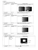
Page 28: ...PUT 1 component input 2 Auto adjustment performance Page 5 26 Bring the cursor on COMP 15K MAIN ADJ and press ENTER COMP 15K ALL ADJ FINISH appears when finished Adjustment item Adjustment conditions Adjustment procedure 1 Adjustment 1080i signal Feed the 100 color bar signal to INPUT 1 component input 2 Auto adjustment performance Page 6 26 Bring the cursor on HDTV ADJ and press ENTER HDTV ADJ FI...

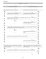
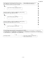
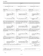
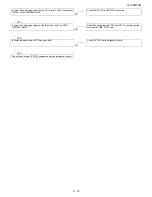
Page 29: ...el Correct the G setting 528 x 6thpoint G setting 928 rounded off and make the R and B settings to their reference levels 6 Set the 2nd point to the specified gradation level Correct the G setting 352 x 6thpoint G setting 928 rounded off and make the R and B settings to their reference levels 7 Set the 1st point to the specified gradation level Correct the G setting 184 x 6thpoint G setting 928 ro...

Page 30: ...ey 6 After the settings are done correctly it is possible to make an adjustment by typing in the command shown in the table below and pressing the ENTER key on the keyboard 7 Command entry is successful if the terminal software indicates OK when the ENTER is pressed If ERR is shown retry to enter the command 8 Send the process mode switching command to switch from the RS232C operation mode to the ...

Page 31: ... on the green background and SUCCESS gets displayed at the top on screen it means the procedure has been successfully car ried out If an error occurs ERROR is displayed on the red background Turn off the AC power Never shut off the power during the initialization process The following settings are initialized in this adjustment 1 User setting 2 Channel data e g broadcast frequencies 3 Password dat...

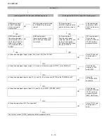
Page 32: ...01 and pin 70 of IC501 AV_SWITCH Check the line between pin 5 of input terminal J502 and pin 76 of IC501 AV_SWITCH Check the line between pin 2 of input terminal J501 and pin 2 of IC501 AV_SWITCH Is there the COMPOSITE video signal input at pin 65 of IC501 AV_SWITCH Is there the COMPOSITE video signal input at pin 71 of IC501 AV_SWITCH Is there the COMPOSITE Video signal input at pins 3 of IC501 A...

Page 33: ...1st channel and 2nd channel of IC3301 TA2_P M AJ30 AK30 TB2_P M AJ29 AK29 TC2_P M AJ28 AK28 TD2_P M AJ26 AK26 TE2_P M AJ25 AK25 TF2_P M AJ24 AK24 TCLK2_P M AJ27 AK27 TA1_P M AB29 AB30 TB1_P M AC29 AC30 TC1_P M AD29 AD30 TD1_P M AF29 AF30 TE1_P M AG29 AG30 TF1_P M AH29 AH30 TF1_P M AH29 AH30 TCLK1_P M AE29 AE30 Check IC3301 and its peripheral con trol circuits IC3501 IC3502 IC8101 etc NO YES Check ...

Page 34: ...PONENT video signal input at pins 21 Y 23 Pb and 25 Pr of IC501 AV_SWITCH Is there the COMPONENT video signal input at pins 27 Y 29 Pb and 31 Pr of IC501 AV_SWITCH Is there the S VIDEO signal input at pins 5 Y and 7 C of IC501 AV_SWITCH YES NO YES NO YES NO Check the line between the input terminals of J501 and IC501 Check the line between the input terminals of J501 and IC501 Check the line betwe...

Page 35: ...01 and IC3301 Q2201 thru Q2203 Q2205 Q2207 Q2209 etc YES Is there the LVDS signal output at the LVDS 1st channel and 2nd channel of IC3301 TA2_P M AJ30 AK30 TB2_P M AJ29 AK29 TC2_P M AJ28 AK28 TD2_P M AJ26 AK26 TE2_P M AJ25 AK25 TF2_P M AJ24 AK24 TCLK2_P M AJ27 AK27 TA1_P M AB29 AB30 TB1_P M AC29 AC30 TC1_P M AD29 AD30 TD1_P M AF29 AF30 TE1_P M AG29 AG30 TF1_P M AH29 AH30 TF1_P M AH29 AH30 TCLK1_P...

Page 36: ...SDA SCL Q8601 NO NO Is there the video signal output at pin 5 of IC1103 LEVEL_ADJ Are there the MPEG signal outputs US_TS_PKTSYNC US_TS_EN US_TS_DATA US_TS_CLK from IC8601 YES NO YES NO Does the level adjustment con trol signal come from pin 6 of IC1103 to pin 1 of IC1104 Check IC8601 and its peripheral control circuits NO Check IC1104 and its peripheral circuits Replace as required Are there the ...

Page 37: ...d 2nd channel of IC3301 TA2_P M AJ30 AK30 TB2_P M AJ29 AK29 TC2_P M AJ28 AK28 TD2_P M AJ26 AK26 TE2_P M AJ25 AK25 TF2_P M AJ24 AK24 TCLK2_P M AJ27 AK27 TA1_P M AB29 AB30 TB1_P M AC29 AC30 TC1_P M AD29 AD30 TD1_P M AF29 AF30 TE1_P M AG29 AG30 TF1_P M AH29 AH30 TF1_P M AH29 AH30 TCLK1_P M AE29 AE30 YES NO Check the panel module Check IC3301 and its peripheral control cir cuits IC3501 IC3502 IC8101 e...

Page 38: ...in 44 of IC1508 HDMI HDCP DVI COMPLI ANT RECEIVER and pin 40 of IC1507 DVI HDMI SWITCH Does the HDMI_PLG_EN signal come from pin 77 of IC9101 to pin 44 of IC1508 HDMI HDCP DVI COMPLI ANT RECEIVER and pin 40 of IC1507 DVI HDMI SWITCH YES NO YES NO Check the line between IC9101 and IC1507 IC1508 Check the line between IC9101 and IC1507 IC1508 Does the HDP2 signal come from pin 62 of IC1507 to pin 19...

Page 39: ...outputs from IC1508 NO Check IC1508 and its peripheral circuits YES Are there the U3VINY 7 0 U3VINR 7 0 U3VINPBPR 7 0 U3VDIN U3HDIN U3DEIN and U3VINCLK signal inputs at IC3301 VPC NO Check the line between IC1508 and IC3301 YES Is there the LVDS signal output at the LVDS 1st channel and 2nd channel of IC3301 TA2_P M AJ30 AK30 TB2_P M AJ29 AK29 TC2_P M AJ28 AK28 TD2_P M AJ26 AK26 TE2_P M AJ25 AK25 ...

Page 40: ... Check the line between SC1503 and IC9101 CPLD Q1501 Q1502 etc Does the HDMI_PLG_EN signal come from pin 77 of IC9101 to pin 44 of IC1508 HDMI HDCP DVI COMPLI ANT RECEIVER and pin 40 of IC1507 DVI HDMI SWITCH YES NO Check the line between IC1901 and IC1507 IC1508 Does the HDP1 signal come from pin 80 of IC1507 to pin 16 of SC1503 NO Check the line between IC1507 and SC1503 Does the signal come fro...

Page 41: ...d its peripheral circuits Are there the U3VINY 7 0 U3VINR 7 0 U3VINPBPR 7 0 U3VDIN U3HDIN U3DEIN and U3VINCLK signal inputs at IC3301 CPU_H8 YES NO Check the line between IC1508 and IC3301 Is there the LVDS signal output at the LVDS 1st channel and 2nd channel of IC3301 TA2_P M AJ30 AK30 TB2_P M AJ29 AK29 TC2_P M AJ28 AK28 TD2_P M AJ26 AK26 TE2_P M AJ25 AK25 TF2_P M AJ24 AK24 TCLK2_P M AJ27 AK27 T...

Page 42: ...audio signal from J502 to SC502 and their peripheral circuits Check the audio signal from J501 to SC502 and their peripheral circuits INPUT 1 Is there the audio signal input at pins 4 L and 2 R of connector SC1102 on the MAIN unit INPUT 2 Is there the audio signal input at pins 8 L and 6 R of connector SC1102 on the MAIN unit INPUT 3 Is there the audio signal input at pins 12 L and 10 R of connect...

Page 43: ...4 connectors YES Is there the audio signal input at pins 5 L and 3 R of IC2701 STEREO_AMP NO Check the line between P2704 and IC2701 and their periph eral circuits AMP_MUTE line YES Is the audio output from IC2701 as specified NO Check IC2701 and its peripheral circuits YES Check the connector P2703 speakers and their peripheral circuits ...

Page 44: ...L and 3 R of input terminal J1502 to pins 55 L and 56 R of IC1404 NO DVI I analog input Check the line between J1502 and IC1404 and their peripheral circuits YES YES Is there the audio signal output at pins 38 L and 39 R of IC1404 NO Check IC1404 and its peripheral cir cuits YES Is there the audio signal output at pins 11 L and 14 R of connector SC1301 on the MAIN unit NO Check the line between IC...

Page 45: ... NO Is the audio output selected for VARIABLE on the menu screen YES Set the audio output to FIXED INPUT 4 If no video appears refer to No exter nal input video HDMI INPUT 4 INPUT 5 If no video appears refer to No exter nal input video HDMI INPUT 5 YES Is the SII9011_MUTE line as specified NO Check Q1301 IC1303 and their peripheral circuits YES Does the HDMI_SPDIF signal come from pin 70 of IC1508...

Page 46: ...1301 YES Is there the audio signal input at pins 11 L and 14 R of connector P2704 on the TERMINAL unit NO Check the SC1301 and P2704 connectors YES Is there the audio signal input at pins 5 L and 3 R of IC2701 STEREO_AMP NO Check the line between P2704 and IC2701 and their periph eral circuits AMP_MUTE line YES Is the audio output from IC2701 as specified NO Check IC2701 and its peripheral circuit...

Page 47: ...eral circuits filter circuit etc Is there the SIF signal input at pins 21 of IC1401 SIF_DECODER NO Check the line between tuner TU1101 and IC1401 and their peripheral circuits Q1102 Q1103 etc YES YES Do the US_TS_CLK DATA EN PKTSYNC signals come from pins 51 59 63 and 66 of IC8601 to pins D11 A9 C10 B10 of IC8101 CPU DECODER NO Check the line between IC8601 and IC8101 and their peripheral circuits...

Page 48: ... main unit NO Check the line between IC1407 and SC1301 and their peripheral circuits YES Are the audio signal inputs at pins 11 L and 14 R of connector P2704 on the TERMINAL unit NO Check the SC1301 and P2704 connectors YES Are the audio signal inputs at pins 5 L and 3 R of IC2701 STEREO_AMP NO Check the line between P2704 and IC2701 and their peripheral circuits AMP_MUTE line YES Is the audio out...

Page 49: ...t etc YES YES Does the HDMI_SPDIF signal come from pin 70 of IC1508 to pin 2 of IC1403 CODEC NO Check the line between IC1508 and IC1403 and their peripheral circuits Do the US_TS_CLK DATA EN PKTSYNC signals come from pins 51 59 63 and 66 of IC8601 to pins D11 A9 C10 B10 of IC8101 CPU DECODER respectively NO Check the line between IC8601 and IC8101 and their peripheral circuits YES YES Is the DTV_...

Page 50: ...nd 4 R of IC1407 BUFF_AMP NO Check the line between IC1403 and IC1407 and their peripheral circuits No optical output under the following conditions as per HDMI require ments Audio contents pro tected Audio frequency beyond 48 KHz Audio bit length beyond 16 bits YES Are the audio signal outputs at pins 1 L and 7 R of IC1407 NO Check IC1407 and its peripheral circuits Replace as required YES Are th...

Page 51: ...ght screen If the panel temperature is 60 C or more for 25 seconds or more in a row error standby is activated MONITOR MAX TEMP on page 23 of process A Change of temperature failure AD value Thermistor Error type Notification LED operation 1 cycle Pins are microprocessor pins unless otherwise specified PS_ON DET_10V failure Flashes once DET_10V pin 63 UR10V or A9V is not applied If error is detect...

Page 52: ...received Main CPU start up failure or monitor microprocessor s recep tion failure Regular communication failure Flashes 3 times Regular communication that is performed at 1 second inter vals in the normal operation is interrupted Main CPU operation failure or monitor microprocessor s reception failure Error type Notification LED operation 1 cycle Basically communication logs are analyzed by a bus ...

Page 53: ...o signals to theater like 5 1 channel sounds Un matrix encoded signals are also con verted to effects rich 5 1 channel output The Tru Surround XT feature creates three dimensional sounds richer than stereo signals 1 6 IC1507 VHiTMDS341A 1Y The TMDS341 single chip IC is provided with multiple switching function in which up to 2 HDMI ports can be selected for a single display input termi nal This 2 ...

Page 54: ...establish communications with the monitor microcomputer in the unit where remote control information or other data is exchanged Another UART is used for RS 232C serial communications to connect the unit to a PC 1 12 IC8301 8302 8303 8304 RH iXB765WJQZQ These are 256 Mb 4 Mb x 16 I O x 4 banks F die DDR SDRAMs 1 13 IC8451 RH iXB963WJQZQ The 64 Mbit page mode flash memory device stores the main CPU ...

Page 55: ...LC 42D72U 5 3 MEMO ...

Page 56: ... 㪋㪈 㪈 㪚㪥㪊 㪉㪇 㪈 㪚㪥㪉 㪈 㪚㪥 㪠㪚㪈 㪤㪘㪠㪥 㪛㪐㪊㪋 㪈 㪋㪈 㪪㪛 㪚㪸㫉㪻 䌈䌄䌍䌉 䌈䌄䌍䌉 㪟㪛㪤㪠 㪘㫌㪻㫀㫆 㪛䊶㪘㩷㪫㫌㫅㪼㫉 㪫㫉㫀㪻㪼㫅㫋 㪣㪯 㪪㪜㪠㪥㪜 㪘㪫㪠 㪈 㪉㪇 㪘㪭㪄㪪㪮 㪘㪤㪧 㪚㫆㫄㫇㫆㫅㪼㫅㫋㪆㪚㫆㫄㫇㫆㫊㫀㫋 㪈㪊 㪈㩷㩷㪋 䇼㪤㪘䇽 䇼㪝㪚䇽 䇼㪪㪘䇽 䇼㪢㪤䇽 䇼㪧㪛䇽 䇼㪧㪟䇽 䇼㪣㪙䇽 䇼㪝㪛䇽 䇼㪣㪭䇽 䇼㪝㪘䇽 䇼㪣㪧䇽 䇼㪩㪘䇽 䇼㪩㪘䇽 䇼㪢㪤䇽 䇼㪪㪧䇽 㪋㪉㩹㪣㪚㪛㩷㪧㪸㫅㪼㫃 㪈㪐㪉㪇㬍㪈㪇㪏㪇 䇼㪪㪣䇽 䇼㪪㪩䇽 㽲 㽳 㽴 㽵 㽷 㽶 㽸 㽺 㪫㪜㪩㪤㪠㪥㪘㪣 㪛㪐㪊㪌 㪈 㪪 㪍 㪈 㪈 㪈㪉 㪈 㪋 㪈 㪌 㪈 㪋 㽹 㪨㪧㪮㪙㪟㪛㪏㪊㪏㪮㪡㪨㪱 㪚㫆㫄㫇㫆㫅㪼㫅㫋㪆㪚㫆㫄㫇㫆㫊㫀㫋 㪨㪚㪥㪮㪄㪜㪏㪐㪏㪮㪡㪨㪱 㪨㪚㪥㪮㪄㪝㪇㪈㪏㪮㪡㪨㪱 㪨㪚㪥㪮㪄㪜㪏㪐㪎㪮㪡㪨㪱 㪨㪚㪥㪮㪄㪝㪇㪈㪎㪮㪡㪨㪱 㪨...

Page 57: ... 㪈 㪉 㪈 㪉 㪈 㪉 㪈 㪍 㪧㪦㪮㪜㪩㵘 㵘 㪬㪥㪠㪠㪫 㪩㪛㪜㪥㪚㪘㪈㪏㪋㪮㪡㪨㪱 㪍 㪈 㪍 㪈 㪣㪚㪛㩷㪚㫆㫅㫋㵘 㪬㪥㪠㪫 㪏㪇 㪈 㪚㪥㪊 㪇㪅㪌㪪㪣㩷㪥㪘㪉㪉㪉 㪏㪇 㪈 㪚㪥㪋 㪇㪅㪌㪪㪣㩷㪥㪘㪉㪉㪉 㪋㪈 㪈 㪚㪥㪊 㪈 㪎 㪚㪥㪌 㪠㪚㪈 㪠㪚㪉 㪌 㪈 㪊 㪈 㪈 㪈㪉 䇼㪣㪘䇽 䇼㪧㪟䇽 䇼㪧㪛䇽 䇼㪝㪛䇽 䇼㪝㪚䇽 㪋㪉㩹㪣㪚㪛㩷㪧㪸㫅㪼㫃 㪈㪐㪉㪇㬍㪈㪇㪏㪇 䇼㪣㪘䇽 㽷 㽶 㽻 㪊 㪈 䇼㪝㪙䇽 䇼㪘㪚䇽 㪉 㪈 㪥㪮㪄㪜㪐㪇㪉㪮㪡㪨㪱 㪮㪄㪜㪉㪌㪏㪮㪡㪨㪱 㪨㪚㪥㪮㪄㪝㪈㪋㪈㪮㪡㪨㪱 㪐 㪈 䇼㪣㪙䇽 ...

Page 58: ...QPX 8 5 4 QORQPGPV WFKQ 0276 0276 0276 0276 0276 8 4 8 4 WFKQ 8 0 4 5 6 241 4 5 6 A GP VCN 68A52 68A 5 2 94 6 0 51 69 4 14 100 614 A 4 2 8 A 1 8 8 8 8 5 0 670 4A8 0 5 2 0 8 5 4 8 2D2T 2D2T 8 8 8 ޣ ޤ 5 5 2 0 8 VQ 0 㪠㪚㪉㪎㪇㪈 㪘㫌㪻㫀㫆㩷㪘㪤㪧 㪫㪧㪘㪊㪈㪇㪇 2 8 8 8 6Q 2 4 4GUGV 6Q KIKVCN 0 68 78 DKV 8 8 8 241 MDKV 8 8 8 2 100 614 14 2 0 100 614 14 7 䇼㪝㪚䇽䋺㪪㪚㪈㪈㪇㪈㪆㪪㪚㪌㪇㪈㩿㪉㪊㪧㪠㪥䋩 䇼㪪㪘䇽䋺㪪㪚㪈㪊㪇㪈㪆㪧㪉㪎㪇㪋㩿㪉㪊㪧㪠㪥䋩 䇼㪪㪧䇽 㪧㪉㪎㪇㪊 㪜㪯㪫㪄㪪㪧...

Page 59: ...8 27 7 46 2 94 6 0 51 69 4 7 614 14 100 614 7 8 4 7 6 2 1 5A5 6 41 5 VCN 219 4 5722 4 7 6 0 5 56 8 8 8 8 8 8 8 8 8 8 GVE 7 8 241 A5 5 9 2 08A 44 241 4 6A20 8 6A 8 GVE 1 56 A219 ޣ ޤ RKP 2 1 1 1 ޣ 5 ޤ 2 RKP A 6 8DTV 7 1 1 1 6 4 1 12 06 4 1 8 A A 59 8 2 8 72 5 56 7 8 7 8 2 A4 3 1 A219 45A10 0 A219 54 5 6 1165 1 1 6 ޣ 4 ޤ 2 R 6 417 74 8 㧔20 X㧕 7 8 ޣ 2 ޤ 219 4 106 2 2 0 7 46 7 46 4GUGV 7 8 4 DKV 2 4 4G...

Page 60: ...LC 42D72U 6 5 3 MAIN BLOCK DIAGRAM ع MAIN BLOCK DIAGRAM ...

Page 61: ...LC 42D72U 6 6 ...

Page 62: ...RMC101 SLD101 R132 R101 D101 IC101 C104 C102 R135 C105 R136 R117 Q105 Q104 R138 R102 D103 R110 R105 R137 R108 Q103 R109 Q102 R106 R104 R107 R123 D114 Q106 R121 R126 D113 Q107 R124 R111 R112 D115 R122 R114 R127 R113 C106 J101 R115 3 R C LED Unit Side A Chip R C LED Unit Side A 1 2 3 4 5 6 7 9 10 8 J A B C D E F G H I ...

Page 63: ...LC 42D72U 7 2 2 KEY UNIT PRINTED WIRING BOARD D155 S157 P151 S153 S151 D151 R151 R152 S152 S154 D152 R153 S155 KEY Unit Side A KEY Unit Side A Chip 1 2 3 4 5 6 7 9 10 8 J A B C D E F G H I ...

Page 64: ...LC 42D72U 7 3 3 MAIN UNIT PRINTED WIRING BOARD MAIN Unit Side A ...

Page 65: ...LC 42D72U 7 4 ...

Page 66: ...LC 42D72U 7 5 MAIN Unit Side A Chip ...

Page 67: ...LC 42D72U 7 6 ...

Page 68: ...LC 42D72U 7 7 MAIN Unit Side B ...

Page 69: ...LC 42D72U 7 8 ...

Page 70: ...LC 42D72U 7 9 MAIN Unit Side B Chip ...

Page 71: ...LC 42D72U 7 10 ...

Page 72: ...LC 42D72U 7 11 4 TERMINAL UNIT PRINTED WIRING BOARD TERMINAL Unit Side A 1 2 3 4 5 6 7 9 10 8 J A B C D E F G H I ...

Page 73: ...586 R576 R578 R579 Q503 R577 Q504 R580 R575 C552 R570 R572 R573 Q501 R569 R571 Q502 R574 C546 C551 C554 FB520 R542 R592 Q509 C557 R591 C524 R543 C575 R590 C525 C538 R559 Q507 R561 R562 C567 C540 R589 D518 R563 Q508 C541 R564 R603 D519 R565 R566 IC501 R604 R609 R608 C543 C545 R607 C544 R601 R567 C542 C523 R568 R537 C530 C529 C527 C526 C564 R541 R540 R539 R610 R538 R536 R605 D512 R549 R548 D511 D510...

Page 74: ...LC 42D72U 7 13 MEMO ...

Page 75: ...F unless otherwise noted P pF µµF 2 All capacitors are 50V unless otherwise noted CAUTION This circuit diagram is original one therefore there may be a slight difference from yours SAFETY NOTES 1 DISCONNECT THE AC PLUG FROM THE AC OUTLET BEFORE REPLACING PARTS 2 SEMICONDUCTOR HEAT SINKS SHOULD BE REGARDED AS POTENTIAL SHOCK HAZARDS WHEN THE CHASSIS IS OPERATING IMPORTANT SAFETY NOTICE PARTS MARKED...

Page 76: ...LC 42D72U 8 2 2 SCHEMATIC DIAGRAM KEY Unit 1 2 3 4 5 6 7 9 10 8 J A B C D E F G H I ...

Page 77: ...LC 42D72U 8 3 R C LED Unit 1 2 3 4 5 6 7 9 10 8 J A B C D E F G H I ...

Page 78: ...LC 42D72U 8 4 MAIN Unit 1 ...

Page 79: ...LC 42D72U 8 5 ...

Page 80: ...LC 42D72U 8 6 MAIN Unit 2 ...

Page 81: ...LC 42D72U 8 7 ...

Page 82: ...LC 42D72U 8 8 MAIN Unit 3 ...

Page 83: ...LC 42D72U 8 9 ...

Page 84: ...LC 42D72U 8 10 MAIN Unit 4 ...

Page 85: ...LC 42D72U 8 11 ...

Page 86: ...LC 42D72U 8 12 MAIN Unit 5 ...

Page 87: ...LC 42D72U 8 13 ...

Page 88: ...LC 42D72U 8 14 MAIN Unit 6 ...

Page 89: ...LC 42D72U 8 15 ...

Page 90: ...LC 42D72U 8 16 MAIN Unit 7 ...

Page 91: ...LC 42D72U 8 17 ...

Page 92: ...LC 42D72U 8 18 MAIN Unit 8 ...

Page 93: ...LC 42D72U 8 19 ...

Page 94: ...LC 42D72U 8 20 ع MAIN Unit 9 ...

Page 95: ...LC 42D72U 8 21 ...

Page 96: ...LC 42D72U 8 22 ع MAIN Unit 10 ...

Page 97: ...LC 42D72U 8 23 ...

Page 98: ...LC 42D72U 8 24 ع MAIN Unit 11 ...

Page 99: ...LC 42D72U 8 25 ...

Page 100: ...LC 42D72U 8 26 ع MAIN Unit 12 ...

Page 101: ...LC 42D72U 8 27 ...

Page 102: ...LC 42D72U 8 28 MAIN Unit 13 ...

Page 103: ...LC 42D72U 8 29 ...

Page 104: ...LC 42D72U 8 30 MAIN Unit 14 ...

Page 105: ...LC 42D72U 8 31 ...

Page 106: ...LC 42D72U 8 32 MAIN Unit 15 ...

Page 107: ...LC 42D72U 8 33 ...

Page 108: ...LC 42D72U 8 34 MAIN Unit 16 ...

Page 109: ...LC 42D72U 8 35 ...

Page 110: ...LC 42D72U 8 36 MAIN Unit 17 ...

Page 111: ...LC 42D72U 8 37 ...

Page 112: ...LC 42D72U 8 38 MAIN Unit 18 ...

Page 113: ...LC 42D72U 8 39 ...

Page 114: ...LC 42D72U 8 40 MAIN Unit 19 ...

Page 115: ...LC 42D72U 8 41 ...

Page 116: ...LC 42D72U 8 42 MAIN Unit 20 ...

Page 117: ...LC 42D72U 8 43 ...

Page 118: ...LC 42D72U 8 44 MAIN Unit 21 ...

Page 119: ...LC 42D72U 8 45 ...

Page 120: ...LC 42D72U 8 46 MAIN Unit 22 ...

Page 121: ...LC 42D72U 8 47 ...

Page 122: ...LC 42D72U 8 48 MAIN Unit 23 ...

Page 123: ...LC 42D72U 8 49 ...

Page 124: ...LC 42D72U 8 50 TERMINAL Unit 1 ...

Page 125: ...LC 42D72U 8 51 ...

Page 126: ...LC 42D72U 8 52 TERMINAL Unit 2 ...

Page 127: ...LC 42D72U 8 53 ...

Page 128: ...LC 42D72U 8 54 MEMO ...

Page 129: ...y The contents are subject to change without notice LC 42D72U PartsGuide 1 PRINTED WIRING BOARD ASSEMBLIES 2 LCD PANEL NOTE THE PARTS HERE SHOWN ARE SUPPLIED AS AN ASSEMBLY BUT NOT INDEPENDENTLY 3 DUNTKD909FM02 R C LED Unit 4 DUNTKD910FM02 KEY Unit 5 DUNTKD934FM10 MAIN Unit 6 DUNTKD935FM11 TERMINAL Unit 7 CABINET PARTS 8 SUPPLIED ACCESSORIES 9 PACKING PARTS NOT REPLACEMENT ITEM 10 SERVICE JIGS USE...

Page 130: ...8W Carbon R152 VRD RA2BE123JY AA J Resistor 12k 1 8W Carbon R153 VRD RA2BE822JY AA J Resistor 8 2k 1 8W Carbon S151 QSW K0003AJZZ AB J Switch CH UP S152 QSW K0003AJZZ AB J Switch CH DOWN S153 QSW K0003AJZZ AB J Switch CH INPUT S154 QSW K0003AJZZ AB J Switch VOL UP S155 QSW K0003AJZZ AB J Switch VOL DOWN S157 QSW K0003AJZZ AB J Switch STANDBY 5 DUNTKD934FM10 MAIN Unit C1101 VCKYCZ1EF104ZY AA J Capa...

Page 131: ... VCKYCZ1EF104ZY AA J Capacitor 0 1 25V Ceramic C1474 VCKYCZ1EF104ZY AA J Capacitor 0 1 25V Ceramic C1475 VCCCCZ1HH101JY AB J Capacitor 100p 50V Ceramic C1476 VCCCCZ1HH101JY AB J Capacitor 100p 50V Ceramic C1477 VCCCCZ1HH6R0DY AA J Capacitor 60p 50V Ceramic C1478 RC KZA510WJPZY AB J Capacitor 10 16V Ceramic C1479 VCKYCZ1EF104ZY AA J Capacitor 0 1 25V Ceramic C1480 VCKYCZ1EF104ZY AA J Capacitor 0 1 ...

Page 132: ...1 VCKYCZ1EF104ZY AA J Capacitor 0 1 25V Ceramic C1572 VCKYCZ1HB102KY AB J Capacitor 1000p 50V Ceramic C1573 VCKYCZ1EF104ZY AA J Capacitor 0 1 25V Ceramic C1574 VCKYCZ1HB102KY AB J Capacitor 1000p 50V Ceramic C1575 RC KZA510WJPZY AB J Capacitor 10 16V Ceramic C1576 VCKYCZ1EF104ZY AA J Capacitor 0 1 25V Ceramic C1577 RC KZA510WJPZY AB J Capacitor 10 16V Ceramic C1578 VCKYCZ1EF104ZY AA J Capacitor 0 ...

Page 133: ...mic C2202 VCCCCZ1HH120JY AB J Capacitor 12p 50V Ceramic C2203 VCCCCZ1HH120JY AB J Capacitor 12p 50V Ceramic C2204 VCCCCZ1HH3R0CY AA J Capacitor 30p 50V Ceramic C2205 VCCCCZ1HH3R0CY AA J Capacitor 30p 50V Ceramic C2206 VCCCCZ1HH270JY AB J Capacitor 27p 50V Ceramic C2207 VCCCCZ1HH270JY AB J Capacitor 27p 50V Ceramic C2208 VCCCCZ1HH120JY AB J Capacitor 12p 50V Ceramic C2209 VCCCCZ1HH3R0CY AA J Capaci...

Page 134: ...YCZ1AB104KY AB J Capacitor 0 1 10V Ceramic C3378 VCKYCZ1AB104KY AB J Capacitor 0 1 10V Ceramic C3379 VCKYCZ1AB104KY AB J Capacitor 0 1 10V Ceramic C3380 VCKYCZ1AB104KY AB J Capacitor 0 1 10V Ceramic C3381 VCKYCZ1AB104KY AB J Capacitor 0 1 10V Ceramic C3382 VCKYCY1AB224KY AB J Capacitor 0 22 10V Ceramic C3383 VCKYCY1AB224KY AB J Capacitor 0 22 10V Ceramic C3384 VCKYCZ1AB104KY AB J Capacitor 0 1 10V...

Page 135: ... 25V Ceramic C8104 VCKYCZ1EF104ZY AA J Capacitor 0 1 25V Ceramic C8105 VCKYCZ1EF104ZY AA J Capacitor 0 1 25V Ceramic C8106 VCKYCZ1EF104ZY AA J Capacitor 0 1 25V Ceramic C8107 VCKYCZ1EF104ZY AA J Capacitor 0 1 25V Ceramic C8108 VCKYCZ1EF104ZY AA J Capacitor 0 1 25V Ceramic C8109 VCKYCZ1EF104ZY AA J Capacitor 0 1 25V Ceramic C8110 VCKYCZ1EF104ZY AA J Capacitor 0 1 25V Ceramic C8111 VCKYCZ1EF104ZY AA...

Page 136: ...C8339 VCKYCZ1EF104ZY AA J Capacitor 0 1 25V Ceramic C8340 VCKYCZ1EF104ZY AA J Capacitor 0 1 25V Ceramic C8341 VCKYCZ1EF104ZY AA J Capacitor 0 1 25V Ceramic C8342 VCKYCZ1EF104ZY AA J Capacitor 0 1 25V Ceramic C8343 VCKYCZ1EF104ZY AA J Capacitor 0 1 25V Ceramic C8344 VCKYCZ1EF104ZY AA J Capacitor 0 1 25V Ceramic C8345 VCKYCZ1EF104ZY AA J Capacitor 0 1 25V Ceramic C8346 VCKYCZ1EF104ZY AA J Capacitor ...

Page 137: ...KYCZ1AB104KY AB J Capacitor 0 1 10V Ceramic C8656 VCKYCZ1AB104KY AB J Capacitor 0 1 10V Ceramic C8657 VCKYCZ1AB104KY AB J Capacitor 0 1 10V Ceramic C8658 VCKYCZ1AB104KY AB J Capacitor 0 1 10V Ceramic C8659 VCKYCZ1AB104KY AB J Capacitor 0 1 10V Ceramic C8660 VCKYCZ1AB104KY AB J Capacitor 0 1 10V Ceramic C8661 VCKYCZ1AB104KY AB J Capacitor 0 1 10V Ceramic C8662 VCKYCZ1AB104KY AB J Capacitor 0 1 10V ...

Page 138: ...V Ceramic C9639 VCKYCZ1AB104KY AB J Capacitor 0 1 10V Ceramic C9640 VCKYCZ1EB822KY AA J Capacitor 8200p 25V Ceramic C9641 VCKYCZ1EB682KY AB J Capacitor 6800p 25V Ceramic C9642 VCKYCZ1HB221KY AA J Capacitor 220p 50V Ceramic C9643 VCKYCZ1HB272KY AA J Capacitor 2700p 50V Ceramic C9644 VCCCCZ1HH101JY AB J Capacitor 100p 50V Ceramic C9645 VCKYCY1EB104KY AB J Capacitor 0 1 25V Ceramic C9646 VCKYTV1CB105...

Page 139: ...AZZY AB X Zener Diode EX0256TA D9606 VHDMA111 1Y AB J Diode MA2J11100L D9607 VHDMA111 1Y AB J Diode MA2J11100L D9608 RH EX1226CEZZY AB J Zener Diode HZU2 4BTRF E 2 4V D9609 VHDMA111 1Y AB J Diode MA2J11100L D9610 RH EX1226CEZZY AB J Zener Diode HZU2 4BTRF E 2 4V D9611 VHDMA111 1Y AB J Diode MA2J11100L D9612 VHDMA111 1Y AB J Diode MA2J11100L D9701 VHDMA111 1Y AB J Diode MA2J11100L D9702 VHDMA111 1Y...

Page 140: ...26111FR1 IC1407 VHiNJM4565V 1Y AF J IC NJM4565V TE1 IC1408 VHiT7SET08U1EY AC J IC TC7SET08FU 5L JF T IC1501 VHi24LC2BiNSES AH R IC HDMI EDID IC1502 VHi24LC2BiNTES AH R IC HDMI EDID IC1503 VHiN74LVC14 1Y AD J IC SN74LVC2G14DCK3 IC1504 VHiT7WH123U 1Y AD J IC TC7WH123FU TE12L F IC1505 RH iXC039WJQZS AH R IC DVI EDID IC1506 VHiPQ018ENA 1Y AF J IC PQ018ENA1ZPH IC1507 VHiTMDS341A 1Y AR J IC TMDS341APFCR...

Page 141: ... 2µH L3303 VPCEM2R2MR23NY AC J Coil Peaking 2 2µH L3304 VPCEM2R2MR23NY AC J Coil Peaking 2 2µH L3305 VPCEM2R2MR23NY AC J Coil Peaking 2 2µH L3306 VPCEM2R2MR23NY AC J Coil Peaking 2 2µH L3307 VPCEM2R2MR23NY AC J Coil Peaking 2 2µH L8601 VPMKMR39JR57VY AB J Coil Peaking 0 39µH L8602 VPMKMR39JR57VY AB J Coil Peaking 0 39µH L8603 VPMKMR33JR50VY AB J Coil Peaking 0 33µH L8604 VPMKMR68JR84VY AB J Coil P...

Page 142: ...05 VRS CZ1JF470JY AA J Resistor 47 1 16W Metal Oxide R1106 VRS CZ1JF331JY AA J Resistor 330 1 16W Metal Oxide R1107 VRS CZ1JF332FY AA J Resistor 3 3k 1 16W Metal Oxide R1108 VRS CZ1JF822FY AA J Resistor 8 2k 1 16W Metal Oxide R1110 VRS CZ1JF683JY AA J Resistor 68k 1 16W Metal Oxide R1111 VRS CZ1JF470JY AA J Resistor 47 1 16W Metal Oxide R1114 VRS CZ1JF102FY AA J Resistor 1k 1 16W Metal Oxide R1121...

Page 143: ...Z1JF220JY AA J Resistor 22 1 16W Metal Oxide R1438 VRS CZ1JF220JY AA J Resistor 22 1 16W Metal Oxide R1439 VRS CZ1JF223FY AA J Resistor 22k 1 16W Metal Oxide R1440 VRS CZ1JF473FY AA J Resistor 47k 1 16W Metal Oxide R1442 VRS CZ1JF000JY AA J Resistor 0 1 16W Metal Oxide R1443 VRS CZ1JF473FY AA J Resistor 47k 1 16W Metal Oxide R1444 VRS CZ1JF101FY AA J Resistor 100 1 16W Metal Oxide R1446 VRS CZ1JF0...

Page 144: ...6 VRS CZ1JF473JY AA J Resistor 47k 1 16W Metal Oxide R1557 VRS CZ1JF103FY AB J Resistor 10k 1 16W Metal Oxide R1559 VRS CZ1JF103FY AB J Resistor 10k 1 16W Metal Oxide R1560 VRS CZ1JF102FY AA J Resistor 1k 1 16W Metal Oxide R1561 VRS CZ1JF330JY AA J Resistor 33 1 16W Metal Oxide R1562 VRS CZ1JF562FY AA J Resistor 5 6k 1 16W Metal Oxide R1563 VRS CZ1JF103FY AB J Resistor 10k 1 16W Metal Oxide R1564 ...

Page 145: ...103FY AB J Resistor 10k 1 16W Metal Oxide R2020 VRS CZ1JF103FY AB J Resistor 10k 1 16W Metal Oxide R2021 VRS CZ1JF103FY AB J Resistor 10k 1 16W Metal Oxide R2023 VRS CZ1JF393FY AA J Resistor 39k 1 16W Metal Oxide R2024 VRS CZ1JF102FY AA J Resistor 1k 1 16W Metal Oxide R2025 VRS CZ1JF103FY AB J Resistor 10k 1 16W Metal Oxide R2029 VRS CZ1JF102FY AA J Resistor 1k 1 16W Metal Oxide R2032 VRS CZ1JF223...

Page 146: ... Oxide R3322 VRS CZ1JF000JY AA J Resistor 0 1 16W Metal Oxide R3323 VRS CZ1JF000JY AA J Resistor 0 1 16W Metal Oxide R3324 VRS CZ1JF100JY AA J Resistor 10 1 16W Metal Oxide R3325 VRS CZ1JF472JY AA J Resistor 4 7k 1 16W Metal Oxide R3326 VRS CZ1JF100JY AA J Resistor 10 1 16W Metal Oxide R3327 VRS CZ1JF472JY AA J Resistor 4 7k 1 16W Metal Oxide R3328 VRS CZ1JF472JY AA J Resistor 4 7k 1 16W Metal Oxi...

Page 147: ...sistor 33 1 16W Metal Oxide R3571 VRS CZ1JF330JY AA J Resistor 33 1 16W Metal Oxide R3572 VRS CZ1JF330JY AA J Resistor 33 1 16W Metal Oxide R3573 VRS CZ1JF330JY AA J Resistor 33 1 16W Metal Oxide R3574 VRS CZ1JF330JY AA J Resistor 33 1 16W Metal Oxide R3575 VRS CZ1JF330JY AA J Resistor 33 1 16W Metal Oxide R3576 VRS CZ1JF330JY AA J Resistor 33 1 16W Metal Oxide R3577 VRS CZ1JF330JY AA J Resistor 3...

Page 148: ...F472JY AA J Resistor 4 7k 1 16W Metal Oxide R8191 VRS CZ1JF472JY AA J Resistor 4 7k 1 16W Metal Oxide R8194 VRS CZ1JF103FY AB J Resistor 10k 1 16W Metal Oxide R8195 VRS CZ1JF103FY AB J Resistor 10k 1 16W Metal Oxide R8196 VRS CZ1JF470JY AA J Resistor 47 1 16W Metal Oxide R8301 VRK CD1JJ680JY AC J Resistor 68 1 16W Metal Composition R8303 VRS CH1JF220JY AA J Resistor 22 1 16W Metal Oxide R8304 VRS ...

Page 149: ... CZ1JF220JY AA J Resistor 22 1 16W Metal Oxide R8395 VRS CZ1JF220JY AA J Resistor 22 1 16W Metal Oxide R8396 VRS CZ1JF220JY AA J Resistor 22 1 16W Metal Oxide R8397 VRS CZ1JF220JY AA J Resistor 22 1 16W Metal Oxide R8398 VRS CZ1JF220JY AA J Resistor 22 1 16W Metal Oxide R8399 VRS CZ1JF220JY AA J Resistor 22 1 16W Metal Oxide R8401 VRS CZ1JF224JY AA J Resistor 220k 1 16W Metal Oxide R8402 VRS CZ1JF...

Page 150: ... 2k 1 16W Metal Oxide R9004 VRS CZ1JF472JY AA J Resistor 4 7k 1 16W Metal Oxide R9005 VRS CZ1JF472JY AA J Resistor 4 7k 1 16W Metal Oxide R9006 VRS CZ1JF472JY AA J Resistor 4 7k 1 16W Metal Oxide R9007 VRS CZ1JF472JY AA J Resistor 4 7k 1 16W Metal Oxide R9010 VRS CZ1JF182FY AA J Resistor 1 8k 1 16W Metal Oxide R9011 VRS CZ1JF182FY AA J Resistor 1 8k 1 16W Metal Oxide R9012 VRS CZ1JF472JY AA J Resi...

Page 151: ...S CZ1JF103FY AB J Resistor 10k 1 16W Metal Oxide R9635 VRS CZ1JF101FY AA J Resistor 100 1 16W Metal Oxide R9636 VRS CZ1JF682FY AA J Resistor 6 8k 1 16W Metal Oxide R9638 VRS CZ1JF473FY AA J Resistor 47k 1 16W Metal Oxide R9639 VRS CZ1JF224JY AA J Resistor 220k 1 16W Metal Oxide R9640 VRS CZ1JF103FY AB J Resistor 10k 1 16W Metal Oxide R9641 VRS CZ1JF682FY AA J Resistor 6 8k 1 16W Metal Oxide R9642 ...

Page 152: ...CKYCH1CB104KY AB J Capacitor 0 1 16V Ceramic C538 VCKYCH1CB104KY AB J Capacitor 0 1 16V Ceramic C540 RC KZA510WJPZY AB J Capacitor 10 16V Ceramic C541 VCKYCH1CB104KY AB J Capacitor 0 1 16V Ceramic C543 VCKYCH1CB104KY AB J Capacitor 0 1 16V Ceramic C544 VCKYCY1EF104ZY AA J Capacitor 0 1 25V Ceramic C545 VCKYCY1EF104ZY AA J Capacitor 0 1 25V Ceramic C546 VCKYCY1EF104ZY AA J Capacitor 0 1 25V Ceramic...

Page 153: ...Diode UDZSTE 1710B 10V D519 RH EX1400CEZZY AB J Zener Diode UDZSTE 1710B 10V D2701 VHDKDS226 1Y AB J Diode KDS226 RTK P FB501 RBLN A204WJZZY AA J Balun FB502 RBLN A204WJZZY AA J Balun FB503 RBLN A204WJZZY AA J Balun FB504 RBLN 0065TAZZY AA J Balun FB505 RBLN 0065TAZZY AA J Balun FB506 RBLN A204WJZZY AA J Balun FB507 RBLN 0065TAZZY AA J Balun FB508 RBLN 0065TAZZY AA J Balun FB509 RBLN A204WJZZY AA ...

Page 154: ...sistor 100 1 16W Metal Oxide R539 VRS CY1JF101JY AA J Resistor 100 1 16W Metal Oxide R540 VRS CY1JF101JY AA J Resistor 100 1 16W Metal Oxide R541 VRS CY1JF101JY AA J Resistor 100 1 16W Metal Oxide R542 VRS CY1JF000JY AA J Resistor 0 1 16W Metal Oxide R548 VRS CY1JF220JY AA J Resistor 22 1 16W Metal Oxide R549 VRS CY1JF220JY AA J Resistor 22 1 16W Metal Oxide R550 VRS CY1JF220JY AA J Resistor 22 1 ...

Page 155: ...or 0 1 16W Metal Oxide R619 VRS CY1JF000JY AA J Resistor 0 1 16W Metal Oxide R2701 VRS CY1JF104JY AA J Resistor 100k 1 16W Metal Oxide R2702 VRS CY1JF104JY AA J Resistor 100k 1 16W Metal Oxide R2705 VRS CY1JF104JY AA J Resistor 100k 1 16W Metal Oxide R2706 VRS CY1JF104JY AA J Resistor 100k 1 16W Metal Oxide R2713 VRS TQ2EF220JY AA J Resistor 22 1 4W Metal Oxide R2714 VRS TQ2EF220JY AA J Resistor 2...

Page 156: ... 3 2 3 61 54 7 48 19 28 43 28 48 6 54 63 5 19 1 50 64 64 65 50 55 50 55 55 19 2 19 2 19 2 55 50 50 2 55 52 16 21 21 49 49 49 49 57 52 2 1 4 4 4 1 4 3 4 2 2 2 49 49 20 49 49 13 55 17 12 50 37 36 59 62 50 10 50 32 60 8 56 39 40 50 58 29 50 41 18 15 53 11 14 30 51 9 27 34 50 45 22 33 49 31 38 35 23 46 44 47 42 22 4 22 2 22 3 22 1 ...

Page 157: ...1 LANGTA401WJFW AT N X Center Angle x2 22 CCHSMA341WJ03 BA N X Tray Chassis Ass y 22 1 Tray Chassis 22 2 LHLDWA102WJKZ AB J Wire Holder 22 3 LHLDWA120WJKZ AB J Wire Holder x4 22 4 LHLDWA123WJKZ AB J Wire Holder x2 23 LHLDW1141CEZZ AE J Wire Holder for LV 27 LHLDWA150WJKZ AC N J Edge Saddle WH 28 LX HZA003WJFN AC J Screw x2 for Speaker 29 LX NZ3047GEZZ AA J Hexiagonal Nut 30 NSFTZ0134CEFW AD J Shaf...

Page 158: ...JKZ AC J Wire Holder X2 LHLDWA083WJ00 AD J Cable Tie X3 LHLDWA131WJKZ AE J Cable Clamp X6 QACCDA039WJPZ AQ J AC Cord X7 RRMCGA535WJSA AY X Remote Control Unit X8 SSAKA0101GJZZ AC X Polyethylene Bag X9 SSAKAA032WJZZ AB J Polyethylene Bag X10 TCADEA208WJZZ AD X Enquete Card X11 TiNS D010WJZZ AQ N X Operation Manual X12 TGAN A768WJZZ AD X Extend Warranty Card X13 CDAi A327WJ02 BN N X Stand Unit X14 A...

Page 159: ...LC 42D72U 31 9 PACKING PARTS NOT REPLACEMENT ITEM S2 S3 S4 S4 S1 S5 S4 S4 ...

Page 160: ...OR SERVICING N QCNW C799WJPZ AG J RCA Cable L 1500mm Tuner Extension N QCNW D483WJQZ AX J 12pins L 1000mm Main Unit to Power Unit PH PA N QCNW E068WJQZ AS J 6pins L 1000mm Main Unit to Power Unit PD MI N QCNW E134WJPZ BG J 41pins L 400mm Main Unit to LCD Controller Unit LV N QCNW F177WJQZ BA J 14pins L 1300mm Main Power Unit to Inverter Unit N QCNW F178WJQZ AW J 20pins L 1000mm Main Unit to LCD Co...

Page 161: ...LC 42D72U ...

Page 162: ...Tochigi 329 2193 Japan COPYRIGHT 2005 BY SHARP CORPORATION ALL RIGHTS RESERVED No Part of this publication may be reproduced stored in a retrieval system or transmitted in any from or by any means electronic mechanical photocopying recording or otherwise without prior written permission of the publisher 2007 ...

Reviews: