2008-03-14
LC-42SB45U
37
↓
YES
<External input 1 / input 2 (Component)>No picture on the display (4)
↓
Does not the picture of the component video signal input (INPUT 1) to Component go out?
Does not the picture of the component video signal input (INPUT 2) to Component go out?
TERMINAL_UNIT:
↓
MAIN_UNIT:
↓
YES
↓
YES
<External input AV3 input 3 (Composite)>No picture on the display (5)
↓
Does not the picture of the composite video signal input to AV3(Composite) go out?
TERMINAL UNIT:
↓
MAIN_UNIT:
↓
YES
↓
YES
<External input AV3 input 3 (Y/C)>No picture on the display (6)
↓
Does not the picture of the Y/C video signal input to AV3(Y/C) go out?
TERMINAL UNIT:
↓
MAIN_UNIT:
↓
YES
Refer to
“
The picture doesn't appear in all modes.
”
Is CVBS signal sent to pin (2) of AV3 (CN650) ?
NO
Check the setting of an external input device that connects of
CN650.
Refer to
“
The picture doesn't appear in all modes.
”
Is CVBS signal sent to pin (AD26) of IC U400?
NO
Check the line between IC U400 and CN650.
Is Y/C signal sent to pin (8)/Y, (7)/C of AV3 (CN650) ?
NO
Check the setting of an external input device that connects of
CN650.
Is Y/C signal sent to pin (AD25)/Y, (AE26)/C of IC U400?
NO
Check the line between IC U400 and CN650.
NO
Is Component Y/Pb/Pr signal sent to pin (2)/Y, (4)/Pb, (6)/Pr of
AV1(CN552) ?
Is Component Y/Pb/Pr signal sent to pin (2)/Y, (4)/Pb, (6)/Pr of
AV1(CN551) ?
NO
Check the setting of an external input device that connects of
CN552.
Check the setting of an external input device that connects of
CN551.
Is Component Y/Pb/Pr signal sent to pin (AD19)/Y, (AF20)/Pb,
(AD20)/Pr of IC U400?
NO
Check the line between IC U400 and CN552
Is Component Y/Pb/Pr signal sent to pin (AE21)/Y, (AE22)/Pb,
(AE23)/Pr of IC U400?
NO
Check the line between IC U400 and CN551.
Refer to
“
The picture doesn't appear in all modes.
”
Summary of Contents for AQUOS LC-42SB45U
Page 6: ...LC 42SB45U 6 TV Front view TV Rear view ...
Page 11: ...2008 03 14 LC 42SB45U 11 3 DIMENSIONS ...
Page 50: ...LC 42SB45U 50 3 2 U102 LP2996MRX PSOP 8 3 2 1 Pin Connections and short description ...
Page 54: ...LC 42SB45U 54 3 8 U402 MX25L3205DMI 12G SOP 16 3 8 1 Block Diagram ...
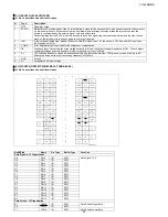
Page 55: ...2008 03 14 LC 42SB45U 55 3 8 2 PIN CONFIGURATION ...
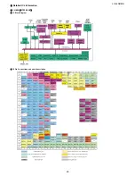
Page 56: ...LC 42SB45U 56 CHAPTER 6 BLOCK DIAGRAM WIRING DIAGRAM 1 MT5382 POWER MAGAGEMENT BLOCK DIAGRAM ...
Page 57: ...2008 03 14 LC 42SB45U 57 2 MAIN BOARD BLOCK DIAGRAM ...
Page 58: ...LC 42SB45U 58 3 WIRING DIAGRAM ...
Page 60: ...60 LC 42SB45U MAIN Unit Side B ...
Page 61: ...LC 42SB45U 1 POWER UNIT PRINTED WIRING BOARD POWER Unit Side A 61 ...
Page 62: ...LC 42SB45U POWER Unit Side B 62 ...
Page 64: ...64 LC 42SB45U IR Unit Side A 3 IR UNIT PRINTED WIRING BOARD IR Unit Side A Cn001 A2 ...


