background image


SERVICE MANUAL

No. S74M52LC-6070LE360X

LED BACKLIGHT TV

LC-60LE360X

 MODEL:

Parts marked with "

" are important for maintaining the safety of the set. Be sure to replace these parts with specified ones for maintaining the

safety and performance of the set.

This document has been published to be used for
after sales service only.
The contents are subject to change without notice.

CHAPTER 1. SAFETY PRECAUTION 

[1]  IMPORTANT SERVICE PRECAUTION ........ 1-1
[2]  PRECAUTIONS FOR USING LEAD-FREE 

SOLDER ........................................................ 1-2

[3] OUTLINE-MAJOR 

SERVICE 

PARTS ............ 1-3

CHAPTER 2. SPECIFICATIONS

[1] SPECIFICATIONS ......................................... 2-1

CHAPTER 3. OPERATION MANUAL 

[1] OPERATION 

MANUAL 

................................. 3-1

CHAPTER 4. DIMENSIONS

[1] DIMENSIONS ................................................ 4-1

CHAPTER 5. REMOVING MAJOR PARTS

[1] REMOVING 

MAJOR 

PARTS ......................... 5-1

CHAPTER 6. ADJUSTMENT

[1] ADJUSTMENT 

.............................................. 6-1

[2]  USB CLONE SPECIFICATIONS.................... 6-8
[3]  PUBLIC MODE SETTING.............................. 6-9

CHAPTER 7. TROUBLESHOOTING TABLE

[1] TROUBLESHOOTING 

TABLE....................... 7-1

CHAPTER 8. SYSTEM BLOCK DIAGRAM

[1]  SYSTEM BLOCK DIAGRAM LC-

60LE360X ...................................................... 8-1

[2]  SYSTEM BLOCK DIAGRAM LC-

70LE360X ...................................................... 8-2

CHAPTER 9. DESCRIPTION OF SCHEMATIC DIA-
GRAM 

[1] DESCRIPTION 

OF SCHEMATIC DIA-

GRAM............................................................9-1

[2]  MAIN UNIT ( LC-60LE360X ) ........................9-2
[3]  MAIN UNIT ( LC-70LE360X ) ......................9-14

Parts Guide

TopPage

CONTENTS

LC-70LE360X

Summary of Contents for Aquos LC-60LE360X

Page 1: ... 1 2 3 OUTLINE MAJOR SERVICE PARTS 1 3 CHAPTER 2 SPECIFICATIONS 1 SPECIFICATIONS 2 1 CHAPTER 3 OPERATION MANUAL 1 OPERATION MANUAL 3 1 CHAPTER 4 DIMENSIONS 1 DIMENSIONS 4 1 CHAPTER 5 REMOVING MAJOR PARTS 1 REMOVING MAJOR PARTS 5 1 CHAPTER 6 ADJUSTMENT 1 ADJUSTMENT 6 1 2 USB CLONE SPECIFICATIONS 6 8 3 PUBLIC MODE SETTING 6 9 CHAPTER 7 TROUBLESHOOTING TABLE 1 TROUBLESHOOTING TABLE 7 1 CHAPTER 8 SYST...

Page 2: ...crew heads knobs and control shafts escutcheon etc and measure the AC voltage drop across the resistor All checks must be repeated with the AC cord plug connection reversed If necessary a nonpolarized adaptor plug must be used only for the purpose of completing these checks Any reading of 0 74 Vrms this corresponds to 0 5 mA rms AC or more is excessive and indicates a potential shock hazard which ...

Page 3: ...n the conventional lead solder by 40 qC and as it has poor solder wettability you may be apt to keep the soldering bit in contact with the PWB for extended period of time However Since the land may be peeled off or the maximum heat resistance temperature of parts may be exceeded remove the bit from the PWB as soon as you confirm the steady soldering condition Lead free solder contains more tin and...

Page 4: ... DUNTKG448FM21 KEY Unit N RUNTKB286WJQZ POWER Unit N DUNTKG476FM02 T CON Unit OTHER UNIT Ref No Part No Description LC 60LE360X N R1JE601D3HA10W 60 TFT LCD Open Cell N CLCDTA375WEA1 60 Panel Assembly Unit LC 70LE360X N R1JE695D3HC50W 70 LCD Panel Module Unit N CLCDTA376WEA1 70 Panel Assembly Unit SERVICE JIGS Ref No Part No Description Q ty N QCNW C222WJQZ Connecting Cord T Con LCD Panel 2 N QCNW ...

Page 5: ... a i s r e P n a i s s u R e s e u g u t r o P h c n e r F c i b a r A e s e n i h C d e fi i l p m i S h s i l g n E e g a u g n a l D S O Thai Vietnamese Indonesia z H 0 6 0 5 V 0 4 2 0 1 1 C A t n e m e r i u q e r r e w o P y b d n a t S W 5 0 W 7 0 2 y b d n a t S W 5 0 W 3 7 1 n o i t p m u s n o c r e w o P Dimensions without stand 1355 W g 786 H g 86 D mm 1563 W g 903 H g 87 D mm with stand...

Page 6: ...re the hook is locked securely 4 For easily user can use polystyrene foam as a jig to hold the stand base when fixing the screws 2 2 Example for left side 2 5 Insert the stand into the openings on the bottom of the TV 3 6 Insert and tighten the screws into the holes on the rear of the TV 4 Soft cushion 4 5 OUTPUT DC5V 1 5A HDMI 4 HDMI 5 USB 2 DC5V 0 5A 5 8 AUDIO IN DIGITAL AUDIO OUTPUT ANALOGUE RGB...

Page 7: ...LC 60 70LE360X 3 2 TV Front POWER indicator Light off Power off Lighted Red The TV is in standby mode Lighted Green The TV is on The illustrations used throughout this manual are based on LC 60LE360X ...

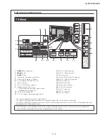
Page 8: ...m The speakers do not output volume when headphones are plugged in 10 INPUT 3 HDMI terminal 11 OUTPUT terminal For power output only 2 12 INPUT 4 HDMI terminal 13 INPUT 5 HDMI terminal 3 14 USB 2 terminal 15 DIGITAL AUDIO OUTPUT terminal 16 INPUT 1 HDMI ARC terminal 17 INPUT 8 terminal 3 18 AUDIO IN terminal 19 Antenna input terminal 20 AUDIO OUT terminals 21 INPUT 7 terminals 22 INPUT 6 terminals...

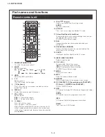
Page 9: ...enu screen 18 MPX Select the sound multiplex mode 19 RETURN MENU mode Return to the previous menu screen 20 m TELETEXT k Reveal hidden for TELETEXT 3 Hold SUBTITLE for TELETEXT Use for TELETEXT mode 21 EPG DTV mode To display EPG Electronic Programme Guide screen GUIDE DTV mode Display the programme channel list INFO DTV mode Display the programme information RADIO Press to access RADIO mode 1 POW...

Page 10: ...LC 60 70LE360X 4 1 CHAPTER 4 DIMENSIONS 1 DIMENSIONS Dimensional drawings 400 400 86 69 350 786 400 400 1355 1332 4 901 825 754 3 1540 6 1563 901 942 871 5 LC 60LE360X LC 70LE360X 87 69 350 903 Unit mm ...

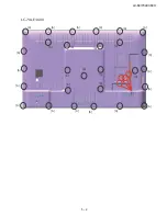
Page 11: ...rew 1 and detech stand unit 2 2 Remove 1 lock screw 3 and detech the AC cord cover 4 3 Disconnect AC Cord 5 4 Remove the 20 lock screws 6 remove 4 screw 7 remove 4 screw 8 LC 60LE360X Remove the 28 lock screws 6 remove 4 screw 7 LC 70LE360X refer next page 5 Detech rear cabinet assmbly 9 1 1 2 2 3 4 5 6 6 6 6 6 6 6 6 6 6 6 6 6 6 6 6 6 6 6 7 7 7 7 6 8 9 LC 60LE360X ...

Page 12: ...LC 60 70LE360X 5 2 LC 70LE360X 6 6 6 6 6 6 6 6 6 6 6 6 6 6 6 6 6 6 6 6 6 6 6 6 6 6 6 6 7 ...

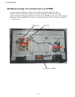
Page 13: ...2 Disconnect the following connectors from the POWER Unit PD PL LED wire 3 Disconnect the following connectors from the LCD CONTROL Unit T Con FFC wayer 4 Remove 4screws 1 Main Unit remove 6 screws 2 Power unit remove 4 screws 3 T CON board MAIN UNIT POWER UNIT T CON LED Wire SP RM KM PD PL T CON FFC WIRE LW LVDS FFC 2 ...

Page 14: ...nction CH CH Changing channel UP DOWN VOL VOL Changing volume UP DOWN Cursor Turning a page PREVIOUS NEXT Cursor Changing a selected line setting 10 10 INPUT button on remote con troller INPUT button Input source switching toggle switching ENTER 3 SoŌware upgrading 1 Make sure LCD TV is on 2 Insert USB device to the USB terminal at the LCD TV Make sure the latest software is installed in the USB d...

Page 15: ... Data Input T CON PWB Checker adjustment Full version confirmation 1 At checker connect software jig at SC6151 TL6151 6157 2 Input voltage at P4804 TL4839 TL4892 and ROM start to input data 3 Power OFF after finish data input Caution item If some error happened ROM data is not written in at all Note Please refer to below for combination of T Con software LCD PANEL T CON UNIT T CON SOFTWARE 1 R1JE6...

Page 16: ... level 㸸0 7Vp p 㸸0 7Vp p s 0 02Vp Com a Adjustment Mode NO E R U D E C O R P N O I T I D N O C M E T I 1 Adjustment Mode Press the test key at the test remote control b Component 15K 50Hz Signal Adjustment COMP SD NO E R U D E C O R P N O I T I D N O C M E T I 1 Setting Signal COMP 15K 50Hz 576i 100 Full field Colour Bar Terminal COMPONENT INPUT 6 Feed the COMPONENT 15K 50Hz 576i 100 Full field Co...

Page 17: ...2 Auto Adjustment Test Mode page 5 COMP HD At the related page move cursor to COMP HD ADJ press ENTER OK appears when finished d PC ANALOG RGB Signal Adjustment PC RGB NO E R U D E C O R P N O I T I D N O C M E T I 1 Setting Signal XGA 60Hz 100 Checkered Pattern Terminal PC INPUT 8 Feed the XGA 60Hz 100 Checkered pattern signal 100 colour saturation to PC INPUT 䈜Please make sure SYNC is OFF 2 Auto...

Page 18: ... gradation for point 2 fix the most faint colour to get reference value adjust others 2 colours to minus adjustment for reference value of point 2 11 Measurement HIGH Brightness Set R_HIGH G_HIGH G_HIGH G_HIGH B_HIGH G_HIGH 12 Calculation MAX luminance after WB ADJ set to Ȗ 2 2 LXHG 13 Set R G B_MAX 14 Calculation LOW luminance Ȗ 2 2 15 Calculation Initial setting of R G B_LOW 16 Set Initial setti...

Page 19: ... R1slope G1slope B1slope between Point2 and Point1 R1slope Rhigh Rlow 3664 480 24 Calculate the correction value پ Rlow پ Glow پ Blow پ Rlow R1slope X 538 480 25 Set the reference value R G B of point 1 R1䇻 R1 پ Rlow 26 Shut down the AC power 䈜Initial value at RGB 2 point 3664 䈜Initial value at RGB 1 point 480 Adjustment value ۼ Teaching set send by engineering dept is set as reference Reference v...

Page 20: ...Q J I Y P B N M X D General 10000 0111 0111 10 B G ENGLISH ITEM E R U D E C O R P N O I T I D N O C Factory setting AC power off to exit the factory setting 1 Setting is done with test remote control 2 Press the Factory Setting key on the remote control continuously 3 When Green background appears on screen and K mark disappears setting is completed The followings are initialised to factory settin...

Page 21: ...to other TVs by using their respective USB terminal 2 How it works 1 Enter USB clone menu Smart Loader i Press panel key INPUT and VOL and AC on it will go to password entry OSD ii Enter digit 369 then it will go to Smart Loader Menu 2 Smart Loader function i SMLD Store To copy all related data from TV USB and put under a fixed filename SHP SMLD bin 8kB ii SMLD Restore To restore the related data fr...

Page 22: ...ower 2 How to exit Public Mode There are the following ways to quit the public mode setup screen Turn off PUBLIC MODE in the adjustment process mode This way alone is not for quitting the setup screen but for quitting the mode by itself Turn off the power with the POWER key Select EXECUTE PUBLIC MODE stays on in the adjustment process mode The settings will be back to the factory ones 3 Public Mod...

Page 23: ...tton is operated a caution is displayed it times out in 5 seconds For the caution refer to the power on fixed message sheet The caution is not displayed when in the adjustment process hotel menu default setting MCL operation and auto preset Ch search operation The OSD display including the menu and this caution have priority over all others When OSD display described below is set to Variable this c...

Page 24: ...ne Exception None Remarks Setting is valid only when Volume fixed is selected for fixed This must be confirmed actually by changing also the sound volume in accordance with setting Selection Selection between Resp ond and No respond loop provide Default Respond Explanation Acceptability of keys by remote control is limited or reception of keys can be prohibited Limit in setting 1 In No respond settin...

Page 25: ...e the operation follows the last memory About options All the input sources in the model are made selectable When the input output switchable input source is selected and the input source is set to output the setting ofinput output switching is changed to input at the execution of hotel menu In addition the input output switching by menu is prohibited In TV mode the display of all channels is stopp...

Page 26: ...n ON Display preset channel plan when power on OFF Not display preset channel plan Default setting Remark When hotel mode is ON and PRESET CHANNEL PLAN is ON press power ON Panel or R C key it displays preset channel plan on the screen When user press ENTER key during TV mode its shows preset channel plan ...

Page 27: ... other cables properly in the set YES Is there the PS ON and PNL POW signal input at pins 10 and 12 of P9602 NO Check the PS ON signal line PNL POW signal line YES Are the DC DC converter outputs and the output voltages along the control lines as specified NO Check the DC DC converters and the control lines Replace defective parts as required 1 M 5 6V IC9601 8 BU 3 3V IC9604 2 D 1 0V IC9612 3 D 5V ...

Page 28: ...ideo onscreen 2 No external input video onscreen INPUT 7 Is INPUT 7 selected on the input select menu screen NO Select INPUT 7 on the input select menu screen to pick up the right input signal YES Is there the video signal input at pin R2 of IC3301 NO Check the line between pin 9 of J502 and pin R2 of IC3301 YES NO Check IC3301 and its peripheral circuits to SC3801 YES Check LVDS cable LCD control...

Page 29: ... H D M I 5 signal input No video onscreen 4 No external input video onscreen INPUT 5 HDMI1 HDMI2 HDMI3 HDMI4 O N YES Are there signal outputs from SC1501 SC1503 to YES s t i u c r i c l a r e h p i r e p s t i d n a 1 0 3 3 C I k c e h C O N s t u p t u o l a n g i s e h t e r e h t e r A YES Check LVDS cable LCD controller incl panel and their periph eral circuits Are there the signal outputs P19...

Page 30: ...O N 2 0 7 1 C I f o 6 n i p t a t u p t n i l a n g i s o i d u a e r e h t s I peripheral circuits YES Is the L ch audio signal output at pin 26 27 NO Check IC1702 and its peripheral circuits of IC1702 normal YES Are the audio signal L ch and R ch output at 3 4 and 1 2 of P1701 normal NO Check circuit between IC1702 P1701 YES Check speakers and their peripheral circuits 30 31 of IC1702 normal Is ...

Page 31: ...n T7 of IC3301 YES Is there the I2S signal output at pin J19 J20 of IC3301 NO Check IC3301 and its peripheral circuits YES O N 2 0 7 1 C I f o 6 n i p t a t u p n i l a n g i s o i d u a e r e h t s I Check connection between IC3301 and IC1702 and its periph eral circuits YES Is the L ch audio signal output at pin 26 27 30 31 of IC1702 normal NO Check IC1702 and its peripheral circuits Is the R ch...

Page 32: ...e r e h t s I Check connection between IC3301 and IC1702 and its periph eral circuits YES Is the L ch audio signal output at pin 26 27 30 31 NO Check IC1702 and its peripheral circuits of IC1702 normal YES Are the audio signal L ch and R ch output at 3 4 and 1 2 of P1702 normal NO Check circuit between IC1702 P1701 YES Check speakers and their peripheral circuits of IC1702 normal Is the R ch audio...

Page 33: ...IC3301 YES C O N 2 0 7 1 C I f o 6 n i p t a t u p n i l a n g i s o i d u a e r e h t s I heck connection between IC3301 and IC1702 and its periph eral circuits YES Is the L ch audio signal outputat pin 26 27 30 31 NO Check IC1702 and its peripheral circuits of IC1702 normal YES Are the audio signal L ch and R ch output at 3 4 and 1 2 of P1701 normal NO Check circuit between IC1702 P1701 YES Chec...

Page 34: ...LC 60 70LE360X 8 1 CHAPTER 8 SYSTEM BLOCK DIA GRAM 1 SYSTEM BLOCK DIAGRAM LC 60LE360X ...

Page 35: ...LC 60 70LE360X 8 2 2 SYSTEM BLOCK DIAGRAM LC 70LE360X ...

Page 36: ...rs are 5 unless otherwise noted K 10 F 1 D 0 5 3 All resistors are 1 16W unless otherwise noted CAPACITOR 1 All capacitors are F unless otherwise noted P pF F 2 All capacitors are 50V unless otherwise noted CAUTION This circuit diagram is original one therefore there may be a slight difference from yours SAFETY NOTES 1 DISCONNECT THE AC PLUG FROM THE AC OUTLET BEFORE REPLACINGPARTS 2 SEMICONDUCTORH...

Page 37: ...3TA C1115 47P CCZ R1107 0 C1148 0 1u C1105 10u 16V R1120 0 CZ R1121 0 CZ C1103 0 1u 25V IF 004 C1147 0 1u TU1102 RTUNQA073WJQZ 1 AT 5V 2 RESET 3 3 3V 4 NC 5 IF_AGC 6 NC 7 NC 8 IF 9 IF 10 SCL 11 SDA C1120 0 1u R1117 470 C1116 47P CCZ C1113 0 1u C1118 0 1u R1102 10K TUN_RF_RESET 004 C1101 1000P 50V R1118 0 C1128 10P C1125 10P 0 47uH L1101 PMT 0 47uH L1102 PMT FB1102 0077TA FB1103 0077TA TO MAIN4 CPU...

Page 38: ...2C_RX 004 RControl R622 100 R623 100 OPT_OUT BU 5V R624 0 FB501 0104TA FB502 0104TA FB511 0104TA FB509 0104TA FB510 0104TA FB514 0104TA FB508 0104TA FB513 0104TA C553 1000P CH C548 1000P CH SC501 NB035WJQZ 1 2 3 4 5 6 7 8 9 10 11 C589 0 1u 25V C585 0 1u C582 10u 16V KZA510WJPZ R553 0 CZ IC511 M3221EIP RS232 TRANSMITTERS RECEIVERS 1 EN 2 C1 3 V 4 C1 5 C2 6 C2 7 V 8 R1_in 9 R1_out 10 NC 11 T1_in 12 ...

Page 39: ... D1513 RB521M30 HDMI0__CLKP 004 HDMI0_D0P 004 HDMI0_DAT 004 Q1506 LTC044EEB HDMI0_D1N 004 R1513 47K CZ HDMI0_HPDIN 004 Q1510 LTC044EEB D1504 RB521M30 R1521 47K 2 1 3 4 HDMI0_D1P 004 HDMI0_CTRL 004 HDMI0__CLKN 004 HDMI0_D2P 004 Q1503 LTC044EEB HDMI0_CLK 004 HDMI0_D2N 004 HDMI_CEC 004 BU 3 3V 010 R1550 10K R1551 10K MHL_CABLE_DET1 004 R1522 300K C1501 0 047u 16V MHL_VBUS_EN1 004 MHL_OCD1 004 AHT1G08...

Page 40: ..._DDR_RESET 005 A_DDR_A0 005 A_DDR_A1 005 A_DDR_A4 005 RXOCP 008 CVBS_AUD_R 002 R3359 4 7K R3363 100 I2S_SCLK 009 SPI_DI 006 R3347 4 7K A_DDR_DQU0 005 A_DDR_DQU1 005 A_DDR_DQU6 005 A_DDR_A5 005 I2C_DAT 001 A_DDR_A7 005 R3367 100 R3355 4 7K R3384 4 7K RXO1N 008 R3380 10 2 1 3 4 A_DDR_DQSL 005 A_DDR_BA1 005 R3381 10 2 1 3 4 SPI_CZ 006 RXO2N 008 R3426 4 7K I2S_LRCLK 009 C3369 100P CCZ R3373 1K C3368 1...

Page 41: ...DR_DQL1 004 A_DDR_DQML 004 A_DDR_A11 004 A_DDR_MCLK 004 A_DDR_DQU3 004 A_DDR_BA1 004 R3505 1K F A_DDR_DQSU 004 D 1 5V 010 A_DDR_A1 004 C3501 1000P 50V K A_DDR_DQL3 004 C3508 1000P 50V R3504 1K F A_DDR_A13 004 A_DDR_A6 004 A_DDR_A4 004 A_DDR_A3 004 A_DDR_BA2 004 A_DDR_A5 004 A_DDR_A12 004 A_DDR_CASZ 004 R3501 1K F A_DDR_A8 004 A_DDR_DQU7 004 A_DDR_BA0 004 A_DDR_DQL0 004 A_DDR_DQL5 004 A_DDR_DQU1 00...

Page 42: ... SPI_WP SPI_WP 004 SPI_CK 004 SPI_DI 004 SPI_DO 004 SPI_CZ 004 BU 3 3V 010 C3104 0 1u 10V CZB TL3114 R3117 4 7K MCP_SPI_CZ 004 MCP_SPI_CK 004 MCP_SPI_DI 004 MCP_SPI_DO 004 W25Q28FV SPI FLASH 1 CS 2 SO SIO1 3 WP 4 GND 5 SI SIO0 6 SCLK 7 HOLD 8 VCC TO MAIN10 POWER TO MAIN4 CPU 2013 09 18 0J MAIN6 FLASH IC3104 QPWBFG455WJ ...

Page 43: ...N 3 PE 4 DET_SYNC 5 R L 6 T_CONSW 7 U D 8 FRAME 9 DET_POW 10 TCON_SCL 11 TCON_SDA 12 LVDS_SEL 13 GND 14 TE2 15 TE2 16 TD2 17 TD2 18 TCLK2 19 TCLK2 20 GND 21 TC2 22 TC2 23 TB2 24 TB2 25 TA2 26 TA2 27 GND 28 TE1 29 TE1 30 TD1 31 TD1 32 TCLK1 33 TCLK1 34 GND 35 TC1 36 TC1 37 TB1 38 TB1 39 TA1 40 TA1 41 GND R3801 10K R3814 0 R3815 0 R3816 100 Soft no control R3807 0 R3809 0 R3821 0 R3822 0 R3823 0 Q38...

Page 44: ...51 10u 16V LINEOUT_RP MON_L_OUT 002 R1748 12K MON_R_OUT 002 FB1708 A371WJQZ FB1709 A371WJQZ R1754 0 C1721 0 1u 25V TPA6139A 1 OUT_L 2 GND 3 GND 4 MUTE 5 VSS 6 CN 7 NC 8 CP 9 VDD 10 GND 11 GAIN 12 OUT_R 13 IN_R 14 NC 15 NC 16 IN_L GND C1722 10u 16V KZA510WJPZ R1766 2 2K C1760 1000P CZB 50V R1765 6 8K R1767 0 CZ C1774 1000P C1775 1000P R1717 7 5K R1781 3 3K C1779 1000P CZB 50V R1782 8 2K R1793 220K ...

Page 45: ... 7K F BU 5V 003 M 5 6V 001 BU 5V 002 S172B50U 1 ON 2 GND 3 N C 4 Vin 5 Vout Q9603 LTC014EEB VS Q9602 LTA014EEB VS E C B M 5 6V 012 D 3 3V 012 D 5V 012 C9628 10u 16V KZA510WJPZ C9601 10u 25V KZA980WJQZ C9602 10u 25V KZA980WJQZ C9603 10u 25V KZA980WJQZ C9627 10u 25V KZA980WJQZ P9602 NB235WJ TO POWER PD 1 PANEL 12V 2 UR 13V 3 UR 13V 4 UR 13V 5 GND 6 GND 7 GND 8 GND 9 DC_DET 10 PS_ON 11 BU5 3V 12 PNL_...

Page 46: ...LC 60 70LE360X 9 11 A C B D E F G H 2 10 9 8 7 6 5 4 3 1 MAIN11 KEY TO MAIN4 CPU 1 5J 2014 03 12 QPWBFGWJZZ DUNTKFWE ...

Page 47: ...004 CI_D1 004 CI_D3 004 CI_D2 004 CI_D6 004 CI_D5 004 CI_D7 004 CI_D4 004 CI_A4 004 CI_A1 004 CI_A0 004 CI_A2 004 CI_A3 004 CI_A6 004 CI_A5 004 CI_RST 004 CI_A12 004 CI_WE 004 CI_CE 004 CI_A9 004 CI_OE 004 CI_IORD 004 CI_IRQA 004 CI_A8 004 CI_A10 004 CI_A11 004 CI_A14 004 CI_A13 004 CI_CD 004 CI_A7 004 DEMOD_TSD1 004 DEMOD_TSD3 004 DEMOD_TSD0 004 DEMOD_TSCLK 004 CI_WAIT 004 CI_REG 004 DEMOD_TSD2 0...

Page 48: ... C2607 0 1u R2625 10 2 1 3 4 C2642 1u CKZ 10V R2689 5 1K C2621 10u 16V R2626 5 1K R2678 5 1 R2530 5 1 R2633 4 7K R2517 10 2 1 3 4 R2501 5 1 R2645 0 R2533 5 1 R2639 10 R2632 4 7K R2674 5 1 R2677 5 1 D 1 0V 010 TL1561 TL1557 TL1560 TL1552 TL1551 TL1542 TL1543 SC1507 ZA321WJQZ Input5 Bottom 1 2 3 4 5 6 7 8 9 10 11 12 13 14 15 16 17 18 19 20 21 22 23 SC1506 ZA321WJQZ Input4 Bottom 1 2 3 4 5 6 7 8 9 10...

Page 49: ...53TA C1115 47P CCZ R1107 0 C1148 0 1u C1105 10u 16V R1120 0 CZ R1121 0 CZ C1103 0 1u 25V IF 004 C1147 0 1u TU1102 RTUNQA073WJQZ 1 AT 5V 2 RESET 3 3 3V 4 NC 5 IF_AGC 6 NC 7 NC 8 IF 9 IF 10 SCL 11 SDA C1120 0 1u R1117 470 C1116 47P CCZ C1113 0 1u C1118 0 1u R1102 10K TUN_RF_RESET 004 C1101 1000P 50V R1118 0 C1128 10P C1125 10P 0 47uH L1101 PMT 0 47uH L1102 PMT FB1102 0077TA FB1103 0077TA TO MAIN4 CP...

Page 50: ...2C_RX 004 RControl R622 100 R623 100 OPT_OUT BU 5V R624 0 FB501 0104TA FB502 0104TA FB511 0104TA FB509 0104TA FB510 0104TA FB514 0104TA FB508 0104TA FB513 0104TA C553 1000P CH C548 1000P CH SC501 NB035WJQZ 1 2 3 4 5 6 7 8 9 10 11 C589 0 1u 25V C585 0 1u C582 10u 16V KZA510WJPZ R553 0 CZ IC511 M3221EIP RS232 TRANSMITTERS RECEIVERS 1 EN 2 C1 3 V 4 C1 5 C2 6 C2 7 V 8 R1_in 9 R1_out 10 NC 11 T1_in 12 ...

Page 51: ...K D1513 RB521M30 HDMI0__CLKP 004 HDMI0_D0P 004 HDMI0_DAT 004 Q1506 LTC044EEB HDMI0_D1N 004 R1513 47K CZ HDMI0_HPDIN 004 Q1510 LTC044EEB D1504 RB521M30 R1521 47K 2 1 3 4 HDMI0_D1P 004 HDMI0_CTRL 004 HDMI0__CLKN 004 HDMI0_D2P 004 Q1503 LTC044EEB HDMI0_CLK 004 HDMI0_D2N 004 HDMI_CEC 004 BU 3 3V 010 R1550 10K R1551 10K MHL_CABLE_DET1 004 R1522 300K C1501 0 047u 16V MHL_VBUS_EN1 004 MHL_OCD1 004 AHT1G0...

Page 52: ..._DDR_RESET 005 A_DDR_A0 005 A_DDR_A1 005 A_DDR_A4 005 RXOCP 008 CVBS_AUD_R 002 R3359 4 7K R3363 100 I2S_SCLK 009 SPI_DI 006 R3347 4 7K A_DDR_DQU0 005 A_DDR_DQU1 005 A_DDR_DQU6 005 A_DDR_A5 005 I2C_DAT 001 A_DDR_A7 005 R3367 100 R3355 4 7K R3384 4 7K RXO1N 008 R3380 10 2 1 3 4 A_DDR_DQSL 005 A_DDR_BA1 005 R3381 10 2 1 3 4 SPI_CZ 006 RXO2N 008 R3426 4 7K I2S_LRCLK 009 C3369 100P CCZ R3373 1K C3368 1...

Page 53: ...DDR_DQL1 004 A_DDR_DQML 004 A_DDR_A11 004 A_DDR_MCLK 004 A_DDR_DQU3 004 A_DDR_BA1 004 R3505 1K F A_DDR_DQSU 004 D 1 5V 010 A_DDR_A1 004 C3501 1000P 50V K A_DDR_DQL3 004 C3508 1000P 50V R3504 1K F A_DDR_A13 004 A_DDR_A6 004 A_DDR_A4 004 A_DDR_A3 004 A_DDR_BA2 004 A_DDR_A5 004 A_DDR_A12 004 A_DDR_CASZ 004 R3501 1K F A_DDR_A8 004 A_DDR_DQU7 004 A_DDR_BA0 004 A_DDR_DQL0 004 A_DDR_DQL5 004 A_DDR_DQU1 0...

Page 54: ... SPI_WP SPI_WP 004 SPI_CK 004 SPI_DI 004 SPI_DO 004 SPI_CZ 004 BU 3 3V 010 C3104 0 1u 10V CZB TL3114 R3117 4 7K MCP_SPI_CZ 004 MCP_SPI_CK 004 MCP_SPI_DI 004 MCP_SPI_DO 004 W25Q28FV SPI FLASH 1 CS 2 SO SIO1 3 WP 4 GND 5 SI SIO0 6 SCLK 7 HOLD 8 VCC TO MAIN10 POWER TO MAIN4 CPU 2013 09 18 0J MAIN6 FLASH IC3104 QPWBFG455WJ ...

Page 55: ...N 3 PE 4 DET_SYNC 5 R L 6 T_CONSW 7 U D 8 FRAME 9 DET_POW 10 TCON_SCL 11 TCON_SDA 12 LVDS_SEL 13 GND 14 TE2 15 TE2 16 TD2 17 TD2 18 TCLK2 19 TCLK2 20 GND 21 TC2 22 TC2 23 TB2 24 TB2 25 TA2 26 TA2 27 GND 28 TE1 29 TE1 30 TD1 31 TD1 32 TCLK1 33 TCLK1 34 GND 35 TC1 36 TC1 37 TB1 38 TB1 39 TA1 40 TA1 41 GND R3801 10K R3814 0 R3815 0 R3816 100 Soft no control R3807 0 R3809 0 R3821 0 R3822 0 R3823 0 Q38...

Page 56: ...751 10u 16V LINEOUT_RP MON_L_OUT 002 R1748 12K MON_R_OUT 002 FB1708 A371WJQZ FB1709 A371WJQZ R1754 0 C1721 0 1u 25V TPA6139A 1 OUT_L 2 GND 3 GND 4 MUTE 5 VSS 6 CN 7 NC 8 CP 9 VDD 10 GND 11 GAIN 12 OUT_R 13 IN_R 14 NC 15 NC 16 IN_L GND C1722 10u 16V KZA510WJPZ R1766 2 2K C1760 1000P CZB 50V R1765 6 8K R1767 0 CZ C1774 1000P C1775 1000P R1717 7 5K R1781 3 3K C1779 1000P CZB 50V R1782 8 2K R1793 220K...

Page 57: ... 7K F BU 5V 003 M 5 6V 001 BU 5V 002 S172B50U 1 ON 2 GND 3 N C 4 Vin 5 Vout Q9603 LTC014EEB VS Q9602 LTA014EEB VS E C B M 5 6V 012 D 3 3V 012 D 5V 012 C9628 10u 16V KZA510WJPZ C9601 10u 25V KZA980WJQZ C9602 10u 25V KZA980WJQZ C9603 10u 25V KZA980WJQZ C9627 10u 25V KZA980WJQZ P9602 NB235WJ TO POWER PD 1 PANEL 12V 2 UR 13V 3 UR 13V 4 UR 13V 5 GND 6 GND 7 GND 8 GND 9 DC_DET 10 PS_ON 11 BU5 3V 12 PNL_...

Page 58: ...LC 60 70LE360X 9 23 A C B D E F G H 2 10 9 8 7 6 5 4 3 1 MAIN11 KEY TO MAIN4 CPU 1 5J 2014 03 12 QPWBFGWJZZ DUNTKFWE ...

Page 59: ..._D1 004 CI_D3 004 CI_D2 004 CI_D6 004 CI_D5 004 CI_D7 004 CI_D4 004 CI_A4 004 CI_A1 004 CI_A0 004 CI_A2 004 CI_A3 004 CI_A6 004 CI_A5 004 CI_RST 004 CI_A12 004 CI_WE 004 CI_CE 004 CI_A9 004 CI_OE 004 CI_IORD 004 CI_IRQA 004 CI_A8 004 CI_A10 004 CI_A11 004 CI_A14 004 CI_A13 004 CI_CD 004 CI_A7 004 DEMOD_TSD1 004 DEMOD_TSD3 004 DEMOD_TSD0 004 DEMOD_TSCLK 004 CI_WAIT 004 CI_REG 004 DEMOD_TSD2 004 DEM...

Page 60: ... C2607 0 1u R2625 10 2 1 3 4 C2642 1u CKZ 10V R2689 5 1K C2621 10u 16V R2626 5 1K R2678 5 1 R2530 5 1 R2633 4 7K R2517 10 2 1 3 4 R2501 5 1 R2645 0 R2533 5 1 R2639 10 R2632 4 7K R2674 5 1 R2677 5 1 D 1 0V 010 TL1561 TL1557 TL1560 TL1552 TL1551 TL1542 TL1543 SC1507 ZA321WJQZ Input5 Bottom 1 2 3 4 5 6 7 8 9 10 11 12 13 14 15 16 17 18 19 20 21 22 23 SC1506 ZA321WJQZ Input4 Bottom 1 2 3 4 5 6 7 8 9 10...

Page 61: ...LC 60 70LE360X 9 26 ...

Page 62: ...ance of the set This document has been published to be used for after sales service only The contents are subject to change without notice LC 60 70LE360X LC 60LE360X LC 70LE360X PartsGuide 1 PRINTED WIRING BOARD ASSEMBLIES 2 LCD PANEL 3 CABINET AND MECHANICAL PARTS LC 60LE360X 4 CABINET AND MECHANICAL PARTS LC 70LE360X 5 LCD PANEL LC 60LE360X 6 LCD PANEL LC 70LE360X 7 SUPPLIED ACCESSORIES 8 PACKIN...

Page 63: ...NIT LC 70LE360X 1 DUNTKG448FM21 V KEY UNIT 1 DUNTKG463FM01 V LED IR UNIT 2 LCD PANEL 1 R1JE601D3HA10W V LCD HIRAKI PANEL UNIT LC 60LE360X 1 CLCDTA375WEA1 V LCD PANEL MODULE UNIT LC 60LE360X 1 R1JE695D3HC50W V LCD HIRAKI PANEL UNIT LC 70LE360X 1 CLCDTA376WEA1 V LCD PANEL MODULE UNIT LC 70LE360X 1 RUNTKB270WJZZ V LED BAR LC 60LE360X 1 RUNTKB273WJZZ V LED BAR LC 70LE360X 1 DUNTKG476FM01 V T CON UNIT ...

Page 64: ...LC 60 70LE360X 3 3 CABINET AND MECHANICAL PARTS LC 60LE360X 1 2 7 18 4 4 1 4 2 2 1 5 5 1 5 2 25 26 27 6 3 3 1 8 8 9 10 MAIN UNIT 40 34 35 22 23 24 20 21 ...

Page 65: ... RA KM HARNESS 22 QCNW P221WJPZ V SP HARNESS 23 QCNW P327WJQZ V T CON FFC 80PIN 24 RCORFA134WJZZ V FFC F CORE 25 RSP ZA706WJZZ V SP L UNIT 26 RSP ZA707WJZZ V SP R UNIT 27 RUNTKB285WJQZ V POWER UNIT 28 XBPS730P06WS0 V FOR ANGLE_PWB 29 XBPS830P08WS0 V FOR CAB B 30 XEBS830P10000 V SCREW FOR COVER 31 ZTAPEP109040E V TAPE 32 ZTAPEP109060E V TAPE 33 HINDPF158WJZZ V SIDE TER LABEL 34 HINDPF159WJZZ V BTM ...

Page 66: ...KM WIRE 26 QCNW P226WJPZ V SP WIRE 27 QCNW P327WJQZ V T CON FFC 80PIN 28 RCORFA134WJZZ V FFC F CORE 29 RSP ZA706WJZZ V SP L UNIT 30 RSP ZA707WJZZ V SP R UNIT 31 RUNTKB286WJQZ V POWER UNIT 32 XBPS730P06WS0 V FOR ANGLE_PWB 33 XBPS830P08WS0 V FOR CAB B 34 XEBS830P10000 V SCREW FOR COVER 35 ZTAPEP109040E V TAPE 36 ZTAPEP109060E V TAPE 26 HINDPF158WJZZ V SIDE TER LABEL 27 HINDPF159WJZZ V BTM TER LABEL ...

Page 67: ...LC 60 70LE360X 6 NO PARTS CODE PRICE RANK NEW MARK PART RANK DESCRIPTION 5 LCD PANEL LC 60LE360X Detail of P Chassis P CHASSIS porom porom 17 1 1 1 6 16 3 5 4 2 11 10 8 13 12 14 ...

Page 68: ...8 ZTAPEP179030E V TAPE 17 30 19 ZTAPEP179065E V Y TAPE 65 17 6 LCD PANEL LC 70LE360X 1 CCHSMA729WJ22 V KS B L CHASSIS 1 1 LCHSMA729WJ2W V B L CHASSIS 2 CHLDZC186WJ21 V KS P CHASSIS TOP L 2 1 LHLDZC186WJ2Z V P CHASSIS TOP L 3 CHLDZC187WJ21 V KS P CHA TOP R 3 1 LHLDZC187WJ2Z V P CHASSIS TOP R 4 CHLDZC190WJ02 V KS P CHA L 4 1 LHLDZC190WJKZ V P CHASSIS L 5 CHLDZC191WJ02 V KS P CHA R 5 1 LHLDZC191WJKZ ...

Page 69: ... TINS G206WJZZ V OPERATION MANUAL I X6 TINS G207WJZZ V OPERATION MANUAL Y X6 TINS G208WJZZ V OPERATION MANUAL P X6 TINS G209WJZZ V OPERATION MANUAL B X6 TINS G210WJZZ V OPERATION MANUAL N X6 TINS G211WJZZ V OPERATION MANUAL M X6 TINS G212WJZZ V OPERATION MANUAL X D X6 TINS G223WJZZ V OPERATION MANUAL Q X7 TGAN B636WJZZ V WARRANTY CARD J X7 TGAN C076WJZZ V WARRANTY CARD I X7 TGAN B383WJN1 V WARRANT...

Page 70: ...NO PARTS CODE PRICE RANK NEW MARK PART RANK DESCRIPTION 8 PACKING PARTS NOT REPLACEMENT ITEM S2 S6 7 S8 REARSIDE Cab BSIDE STANDBASE R STANDBASE L FRONT S4 X4 X4 S9 S10 S3 S12 S1 S5 S11 S13 X3 X1 X2 X5 X6 X7 X8 S14 S15 ...

Page 71: ... LC 70LE360X S4 SPAKPB733WJ4Z HOSO PP S5 SPAKXE362WJZZ TOP AD L S6 SPAKXE366WJZZ BTM AD L S7 SPAKXE367WJZZ BTM AD C S8 SPAKXE368WJZZ BTM AD R S9 SPAKXE364WJZZ SIDE AD L LC 60LE360X S9 SPAKXE369WJZZ SIDE AD L LC 70LE360X S10 SPAKXE365WJZZ SIDE AD R LC 60LE360X S10 SPAKXE370WJZZ SIDE AD R LC 70LE360X S11 SPAKXE363WJZZ TOP AD C LC 60LE360X S11 SPAKXE380WJZZ TOP AD C LC 70LE360X S12 SPAKXE436WJZZ FRON...

Page 72: ...LC 60 70LE360X 11 ...

Page 73: ...rt of this publication may be reproduced stored in a retrieval system or transmitted in any form or by any means electronic mechanical photocopying recording or otherwise without prior written permission of the publisher COPYRIGHT XXXX BYSHARP CORPORATION ALL RIGHTS RESERVED COPYRIGHT 2014 BY SHARP CORPORATION SHARP MANUFACTURING CORPORATION M SDN BHD PQA DEPARTMENT Batu Pahat Johor Malaysia RQ241...

Reviews: