background image

CONFIDENTIAL – DO NOT COPY


Page 2-3


File No. SG-0000351


(7) When the surface becomes dusty, please wipe gently with absorbent cotton or 

other soft materials like chamois soaks with petroleum. Normal-hexane is 
recommended for cleaning the adhesives used to attach front / rear polarity. 
Do not use acetone, toluene and alcohol because they cause chemical 
damage to the polarizer. 

(8) Wipe off saliva or water drops as soon as possible. Their long time contact 

with polarizer causes deformations and color fading. 

(9) Do not open the case because inside circuits do not have sufficient strength. 
 

9-2. Operating Precautions 

(1) The spike noise causes the miss operation of circuits. It should be lower than 

following voltage: 

V=±200mV (Over and under shoot voltage) 

(2) Response time depends on the temperature. (In lower temperature, it 

becomes longer.) 

(3) Brightness depends on the temperature. (In lower temperature, it becomes 

lower.) And in lower temperature, response time (required time that brightness 
is stable after turned on) becomes longer. 

(4) Be careful for condensation at sudden temperature change. Condensation 

makes damage to polarizer or electrical contacted parts. And after fading 
condensation, smear or spot will occur. 

(5) When fixed patterns are displayed for a long time, remnant image is likely to 

occur. 

(6) Module has high frequency circuits. Sufficient suppression to the 

electromagnetic interference shall be done by system manufacturers. 
Grounding and shielding methods may be important to minimize the 
interference. 

(7) Please do not give any mechanical and/or acoustical impact to LCM. 

Otherwise, LCM can’t be operated its full characteristics perfectly. 

(8) A screw which is fastened up the steels should be a machine screw. (if not, it 

causes metallic foreign material and deal LCM a fatal blow) 

(9) Please do not set LCD on its edge. 
 

9-3. Electrostatic Discharge Control 

Since a module is composed of electronic circuits, it is not strong to electrostatic 
discharge. Make certain that treatment persons are connected to ground through 
wrist band etc. And don’t touch interface pin directly. 

Summary of Contents for Aquos LC-65LE654U

Page 1: ...Service Manual Top Confidential Model LCD TV 65 LC 65LE654U_RTD2986Id AUO T650HVN05 502 ...

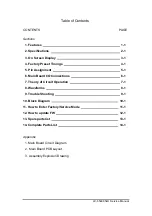
Page 2: ...5 Pin Assignment 5 1 6 Main Board I O Connections 6 1 7 Theory of Circuit Operation 7 1 8 Waveforms 8 1 9 Trouble Shooting 9 1 10 Block Diagram 10 1 11 How to Enter Factory Service Mode 11 1 12 How to update FW 12 1 13 Spare parts list 13 1 14 Complete Parts List 14 1 Appendix 1 Main Board Circuit Diagram 2 Main Board PCB Layout 3 Assembly Explosion Drawing ...

Page 3: ...communications However there is no guarantee that the interference will not occur in a particular installation If this equipment does cause unacceptable interference to radio or television reception which can be determined by turning the equipment off and on the user is encouraged to try to correct the interference by one or more of the following measures reorient or relocate the receiving antenna...

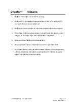
Page 4: ...for automatic adjustment of screen display 4 Smoothing function enables display of smooth texts and graphics even if image with resolution lower than 1920x1080 is magnified 5 Advanced video functions for personal favor 6 Power saving to reduce consumption power too less than 0 5W 7 On Screen Display user can define display mode i e color brightness contrast sharpness back light sound setting TV ch...

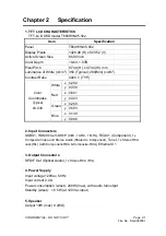
Page 5: ... TYP x 0 292 White y 0 339 x 0 661 Red y 0 323 x 0 269 Green y 0 593 x 0 139 Color Coordinates Typical 0 030 Blue y 0 088 2 Input Connectors USBX1 HDMIX3 with HDCP CEC 1 ARC 1 MHL RCAX1 Component 1x Composite Video and Stereo Audio Shared to Component Tuner 1x Stereo RCA Jack R L with Component RCA Composite RCA Ethernet X1 3 Output Connectors SPDIF Out Optical Audio 1x Stereo RCA R L 4 Power Supp...

Page 6: ...h a module is mounted should have sufficient strength so that external force is not transmitted directly to the module 3 Please attach the surface transparent protective plate to the surface in order to protect the polarizer Transparent protective plate should have sufficient strength in order to the resist external force 4 You should adopt radiation structure to satisfy the temperature specificat...

Page 7: ...esponse time required time that brightness is stable after turned on becomes longer 4 Be careful for condensation at sudden temperature change Condensation makes damage to polarizer or electrical contacted parts And after fading condensation smear or spot will occur 5 When fixed patterns are displayed for a long time remnant image is likely to occur 6 Module has high frequency circuits Sufficient ...

Page 8: ... 9 6 Handling Precautions for Protection Film 1 The protection film is attached to the bezel with a small masking tape When the protection film is peeled off static electricity is generated between the film and polarizer This should be peeled off slowly and carefully by people who are electrically grounded and with well ion blown equipment or in such a condition etc 2 When the module with protecti...

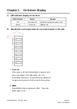
Page 9: ...n When power is off and the Side button is pressed upon press not release of the Side button the TV is immediately powered on Long and short key presses do not apply when power is off at the time of the key press ii MENU Press MENU button to activate the OSD Press this button again to exit LED indicator Status Remark Off AC power off By disconnecting the power cord White Power on Default off ...

Page 10: ... maximum At the time volume should increase with VOL button and decrease with VOL button and volume shift should be smooth When the OSD is activated it can be navigated left and right by operating these two buttons v Input Change Confirmation This button allows the user to cycle through the input sources in the following sequence TV AV Component HDMI 1 HDMI 2 HDMI_SIDE When the OSD is activated th...

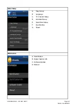
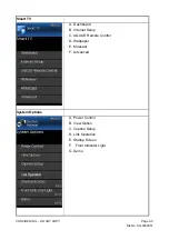
Page 11: ... Page 3 3 File No SG 0000351 Initial Setup A Easy Setup B Language C TV Channel Setup D Individual Setup E Quick Start Mode F Input Setting G Reset Information A Identification B Digital Caption Info C Software Update D Manual ...

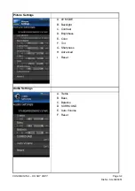
Page 12: ...OT COPY Page 3 4 File No SG 0000351 Picture Settings A AV MODE B Backlight C Contrast D Brightness E Color F Tint G Sharpness H Advanced I Reset Audio Settings A Treble B Bass C Balance D SURROUND E Auto Volume F Reset ...

Page 13: ...le No SG 0000351 Smart TV A Dashboard B Internet Setup C AQUOS Remote Control D Wallpaper E Miracast F Advanced System Options A Power Control B View Option C Caption Setup D Link Operation E Startup Screen F Front Indicator Light G Demo ...

Page 14: ...CONFIDENTIAL DO NOT COPY Page 3 6 File No SG 0000351 INPUT A TV B HDMI1 C HDMI2 D HDMI3 E COMPONENT Video F USB G Home Network H Miracast USB Content Example Home Network Content Example ...

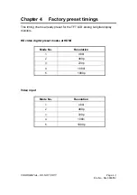
Page 15: ...ctory preset timings This timing chart is already preset for the TFT LCD analog digital display monitors HD video digital preset modes at HDMI Mode No Resolution 1 480i 2 480p 3 720p 4 1080i 5 1080p Video input Mode No Resolution 1 480i 2 480p 3 720p 4 1080i 5 1080p ...

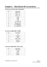
Page 16: ...1 7 TMDS Data0 8 TMDS Data0 Shield 9 TMDS Data0 10 TMDS Clock 11 TMDS Clock Shield 12 TMDS Clock 13 CEC 14 Reserved N C on device 15 SCL 16 SDA 17 DDC CEC Ground 18 5V Power 19 Hot Plug Detect HDMI Signal HDMI a Pin Assignment Refer to HDMI Pin Assignment b Type A c Polarity Positive or Negative d Frequency H 15 734KHz V 60Hz NTSC 480i H 31KHz V 60Hz NTSC 480p H 45KHz V 60Hz NTSC 720p H 33KHz V 60...

Page 17: ... Connector a Frequency H 15 734KHz V 60Hz NTSC b Signal level Video Y C 1Vp p Sync H V 0 3V below Video Y C c Impedance 75Ω d Connector type RCA Jack Component video Connector a Frequency H 15 734KHz V 60Hz NTSC 480i H 31KHz V 60Hz NTSC 480p H 45KHz V 60Hz NTSC 720p H 33KHz V 60Hz NTSC 1080i H 67 5KHz V 60Hz NTSC 1080P b Signal level Y 1Vp p Pb 0 350Vp p Pr 0 350Vp p c Impedance 75Ω d Connector ty...

Page 18: ...igital Audio Out Optical a Peak emission wave length 630 690 nm b Transmission Speed 16M bps Max c Connector type Optical fiber transmitter Analog Audio Out a Signal level 2Vrms Max b Impedance 600Ω c Frequency response 20Hz 20KHz d Connector type RCA L R ...

Page 19: ...d to Main BD Pin Description 1 PWR_19V 2 PWR_19V 3 PWR_19V 4 GND 5 GND 6 GND 7 12V_ON_OFF 8 BL_ON_OFF 9 BL_DIMMING1 10 BL_DIMMING2 J13 CONNECTION MAIN BD TO IR BD Pin Description 1 IR 2 IR_Power 3 GND 4 WHITE_LED 5 LS_SCL 6 LS_SDA JI3 CONNECTION MAIN BD TO DISPLAY BD Pin Description 1 IR_Power 2 GND 3 ADIN1 4 ADIN0 ...

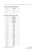
Page 20: ... SPEAKER Pin Description 1 R 2 R 3 L 4 L JM4 CONNECTION MAIN BD TO PANEL SIDE Pin Description 1 LVDSVDD 2 LVDSVDD 3 LVDSVDD 4 LVDSVDD 5 LVDSVDD 6 NC 7 GND 8 GND 9 NC 10 GND 11 B4M 12 B4P 13 B3M 14 B3P 15 GND 16 BCKM 17 BCKP 18 GND 19 B2M 20 B2P 21 B1M 22 B1P 23 B0M 24 B0P 25 GND ...

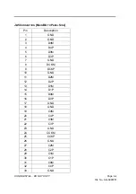
Page 21: ...Page 6 3 File No SG 0000351 26 GND 27 A4M 28 A4P 29 A3M 30 A3P 31 GND 32 ACKM 33 ACKP 34 GND 35 A2M 36 A2P 37 A1M 38 A1P 39 A0M 40 A0P 41 GND 42 NC 43 NC 44 NC 45 LVDS_FORMAT 46 NC 47 NC 48 Tcon_SDA 49 Tcon_WP 50 Tcon_SCL 51 NC ...

Page 22: ...ON MAIN BD TO PANEL SIDE Pin Description 1 GND 2 GND 3 D4M 4 D4P 5 D3M 6 D3P 7 GND 8 DCKM 9 DCKP 10 GND 11 D2M 12 D2P 13 D1M 14 D1P 15 D0M 16 D0P 17 GND 18 GND 19 C4M 20 C4P 21 C3M 22 C3P 23 GND 24 CCKM 25 CCKP 26 GND 27 C2M 28 C2P 29 C1M 30 C1P 31 C0M 32 C0P 33 GND ...

Page 23: ...CONFIDENTIAL DO NOT COPY Page 6 5 File No SG 0000351 34 NC 35 NC 36 NC 37 NC 38 NC 39 NC 40 NC 41 NC ...

Page 24: ...ating signal is divided into two parts video and audio signal The video signal is processed by RTD2986ID then RTD2986ID generates a LVDS for display device The audio signal is transmitted in the route named SIF The SIF signal is demodulated and decoded by RTD2986ID The audio signal is inputted RTD2986ID RTD2986ID transmits the signal to audio amplifier Then the amplified signal is the output audio...

Page 25: ...ormance RISC CPU to manipulate all possible routines and house keeping activities With extendable USB 2 0 interface an RTD2986ID based system can turn into a high quality media center in a simple manner RTD2986ID enables feature rich products that bring differentiation to the iDTV market By the use of powerful CPU GPU and AV decoders capable of decoding a plethora of high definition content from E...

Page 26: ...in 8Ch One SPDIF in and SPDIF out supported Non PCM SPDIF output Support HDMI 1 4 ARC Video Input Output 3 Ch HDMI 1 4a compliant receiver Support HDMI 1 4a 3D mandatory format Support HDMI 1 4a 4K2K 30Hz format Support HDMI CEC interface Support 1 ports YPrPb video input up to 1080p with Sync Processor 480i 576i 480p 576p 720p 1080i 1080P Support 1 port VGA input up to ADC 170MHz up to 1600x1200 ...

Page 27: ... ITU R BT 119 method IEC 61880 method CC XDS method WSS ETSI EN 300 294 ITU R BT 119 method IEC 61880 method CC XDS method TT Tele Text 1 5 2 5 ETSI EN 300 706 ATV IF Demodulation Fully Support NTSC PAL SECAM IF Demodulation Multi standard true synchronous demodulation with active carrier regeneration Normal IF and Low IF input supported VIF AGC detector for gain control Programmable TOP to accomm...

Page 28: ... channel to two channel Support compressed audio passing through SPDIF Support Dolby digital plus to Dolby transcode and output to SPDIF Audio Post Processing Hardwired Automatic Volume Control 7 stage Equalizer Treble Bass Loudness Volume Balance control RealStereo RealSurround RealSpace RealVoice RealEnvironment Dynamic Speaker Image Processor Input format detection and Smart FitTM Compatibility...

Page 29: ...z Over Drive function Support local dimming for direct edge backlight LED panel Embedded TCON flexible timing control with programmable timing Memory Interface Support SPI Flash NAND flash eMMC Configurable flash access timing Support SPI flash boot or NAND flash or eMMC boot DDR3 embedded Peripheral Interface Support two 16550 UARTs each has 16 byte FIFO Support one IrDA Rx interface which compli...

Page 30: ...ristics Recommended Operating Conditions Parameter Symbol Min Typ Max Units 3 3V Supply Voltages VVDD_33 3 13 3 3 3 47 V 1 5V Supply Voltages VVDD 15 1 42 1 5 1 58 V 1 15V Supply Voltages VVDD_115 1 115 1 15 1 185 V Ambient Operating Temperature TA 0 70 C Junction Temperature TJ 125 C Absolute Maximum Ratings Parameter Symbol Min Typ Max Units 3 3V Supply Voltages VVDD_33 3 47 V 1 8V Supply Voltag...

Page 31: ...CONFIDENTIAL DO NOT COPY Page 7 8 File No SG 0000351 Flash MT29F4G08ABAEAWP ...

Page 32: ...CONFIDENTIAL DO NOT COPY Page 7 9 File No SG 0000351 ...

Page 33: ...CONFIDENTIAL DO NOT COPY Page 7 10 File No SG 0000351 ...

Page 34: ...CONFIDENTIAL DO NOT COPY Page 7 11 File No SG 0000351 ...

Page 35: ...CONFIDENTIAL DO NOT COPY Page 7 12 File No SG 0000351 ...

Page 36: ...CONFIDENTIAL DO NOT COPY Page 7 13 File No SG 0000351 ...

Page 37: ...CONFIDENTIAL DO NOT COPY Page 7 14 File No SG 0000351 ...

Page 38: ...CONFIDENTIAL DO NOT COPY Page 7 15 File No SG 0000351 ...

Page 39: ...CONFIDENTIAL DO NOT COPY Page 7 16 File No SG 0000351 ...

Page 40: ...CONFIDENTIAL DO NOT COPY Page 7 17 File No SG 0000351 ...

Page 41: ...CONFIDENTIAL DO NOT COPY Page 7 18 File No SG 0000351 Audio Amplifier TAS5707L ...

Page 42: ...CONFIDENTIAL DO NOT COPY Page 7 19 File No SG 0000351 ...

Page 43: ...ing edge technology include Content Adaptive MEMC significantly reduces film judder and blur caused by slow LCD response time Support for up to 100Hz 120Hz refresh rate at 1080p and WUXGA resolutions Integrated support for Pixelworks proprietary motion adaptive 2D to 3D conversion Integrated Overdrive to improve pixel response time and reduce ghosting Proprietary n2m adaptive frame rate conversion...

Page 44: ... film mode detection with 3 2 2 2 inverse pull down and programmable random cadence detection Support for horizontal and vertical flip and 180 degree rotation 10 bit Full HD Video processing in 4 2 2 format 10 bit graphics in 4 4 4 format Integrated Overdrive Programmable OSD region protection up to 5 OSD regions Automatic OSD logo detection and protection Support for demo modes Input Port 24 30 b...

Page 45: ...ith Dithering Color space conversion Support for xvYCC color space Support for BT 601 and BT 709 LED Backlight Control Advanced Local Dimming algorithm Black frame insertion Output Port 4 channel LVDS transmitter up to 1 050Mbps per channel Supports dual frame output Support for Spread spectrum Color Management Full support for xvYCC color space Hue and flesh tone correction Color and saturation e...

Page 46: ...CONFIDENTIAL DO NOT COPY Page 7 23 File No SG 0000351 PA136PD Internal Block Diagram Pin Descriptions ...

Page 47: ...CONFIDENTIAL DO NOT COPY Page 7 24 File No SG 0000351 Packaging ...

Page 48: ...CONFIDENTIAL DO NOT COPY Page 7 25 File No SG 0000351 ...

Page 49: ...CONFIDENTIAL DO NOT COPY Page 7 26 File No SG 0000351 Electrical Specifications Absolute Maximum Ratings Absolute Maximum Ratings Continued Electrical Specification for Power DC Specifications ...

Page 50: ...CONFIDENTIAL DO NOT COPY Page 7 27 File No SG 0000351 DC Specifications Continued DC Specifications Continued ...

Page 51: ...CONFIDENTIAL DO NOT COPY Page 8 1 File No SG 0000351 Chapter 8 Waveforms HDMI TMDS 1080I input CH2 CLK CH3 CLK TMDS 1080P input CH2 CLK CH3 CLK ...

Page 52: ...CONFIDENTIAL DO NOT COPY Page 8 2 File No SG 0000351 YCbCr 1 100 color bar 標準信號 Component _ Y Component _ Pb Component _ Pr 2 最高頻的 timing 訊號為1黑 1 白或 multi burst 訊號 for CVBS Component _ Y ...

Page 53: ...CONFIDENTIAL DO NOT COPY Page 8 3 File No SG 0000351 Component _ Pb Component _ Pr 3 25 gray 訊號 Component _ Y DC_ON Component _ Y DC_OFF Component _ Pb DC_ON Component _ Pb DC_OFF ...

Page 54: ...CONFIDENTIAL DO NOT COPY Page 8 4 File No SG 0000351 Component _ Pr DC_ON Component _ Pr DC_OFF ...

Page 55: ...l good 1 Check video 2 Check DVD player U401 input correct 1 Check VIDEO signal 2 Check signal between U401 IF IN AV mode LVDS output correct 1 Check power system U401 3V3SB 3 3V 1 15V 1 5V_DDR2 2 Check Y1 s frequency is OK 1 Check JM4 JM5 Connect is good 2 Is panel working ok END U401 output correct 1 Check mini LVDS cable 2 Check U401 clock 27MHz 3 Check LVDS signal ...

Page 56: ...FIDENTIAL DO NOT COPY Page 9 2 File No SG 0000351 Yes N0 HDMI IS NOT DISPLAY CORRECTLY Input signal good Start 1 Check video 2 Check host s setting 1 Are JM4 and JM5 connected ok 2 Is panel working ok END ...

Page 57: ...he voltage is V33 Yes Yes Yes Yes Yes N0 N0 N0 N0 N0 N0 The voltage is V25 N0 The voltage is DDRV18 N0 The voltage is V10 N0 Yes Yes Yes TROUBLE OF DC DC CONVERTER Start CP10 CPE9 The voltage is 19V 1 Check power connection JP1 C457 The voltage is 12V QP4 Pin3 CMP20 END CPE7 JP1 PIN1 The voltage is 1 15V FBP5 CMP5 CMP25 ...

Page 58: ...OT DISPLAY CORRECTLY Start Input signal good 1 Check Audio source 2 Check the player of source Input correct 1 Check signal of Main Board 2 Check 12V of LA1 3 Check 3 3V of LA2 Check amplifier OK END Check signal correct 1 Check RTD2986ID audio out RTD2986ID Pin42 Pin45 1 Check amplifier UA1 ...

Page 59: ...ut SPDIF OUT SPDIF OUT TAS5707LPHP PH6 U401 RTD2986ID USB SIDE HDMI IR POWER INDICATOR J13 J1 YPbPr UART HDMI MHL Factory USB CVBS PA1 JA1 PA2 SPEAKER OUT SPEAKER AMP UW1 NPCA110DA0YX Wave Audio DSP HDMI_2_RX PH4 DOWN HDMI VIFP VIFM HDMI ARC HDMI_1_RX UT3 PH5 DOWN HDMI HDMI HDMI_0_RX USB0_D D IIS IIS PU3 NAND FLASH US3 1Gbit NAND FLASH INTERFACE Block Diagram PA136 WIFI MODULE JU4 ETHERNET JN1 LVD...

Page 60: ...13 LP2 2 2uH 1 15V FBT1 BEAD UT3 UT4 TUNER TUNER_3V3 PU3 USB CONN 500mA Irms 564mA Imax 1 57A UM3 AT24C02BN SH T LMP1 2 2uH UMP2 LA8013 PV18 Irms 193mA Imax 440mA FBP5 BEAD UMP1 AX6646BTA V25 Irms 228mA Imax 306mA D3V3 A3V3 950mA PH6 HDMI CONN UM3 W9751G6JB 25 V10 Irms 833mA Imax 1 48A D1V1 M3V3 Imin 280mA Imin 300mA Imin 280mA Irms 1 51A Imax 4 38A 12V Imin 200mA Imin 400mA Imin 410mA Imin 1 43A ...

Page 61: ...on RC to show the Main Menu 3 Enter the Factory Menu 4 digits password 2 4 8 9 to show Factory Menu NOTE DO NOT Select EXIT while in Factory Mode MUST select CLEAN STORAGE under SET UP to EXIT properly Enter Service Menu 1 Set theTV under an input source A TV AV IN Component or HDMI B Not in the Setup Wizard or MMP 2 Press MENU key on RC to show the Main Menu 3 Enter the Service Menu 4 digits pass...

Page 62: ... into the USB Flash Stick 3 Unplug the AC cable from the TV let TV power off No AC power 4 Insert the USB flash stick to TV 5 Plug in the AC cable 6 TV will start to read USB stick and update the firmware DO NOT unplug AC cable or remove USB stick when the LED indicator is blinking 7 After the LED indicator stop blinking remove the USB stick 8 FW Update complete TV can be power on ...

Page 63: ...00443 WAFER 2 50mm 4P 90 KINK A2501WR2 4P L F 1 JA1 S 9LE 045125000449 WAFER 2 50mm 4P 90 KINK A2501WR 04P1 L F 1 JA1 S 9LE 030480000240 RJ45 CONN 90 Without LED 5450 025 1G3 A9 LF 1 JN1 9LE 030062000051 USB CONN A TYPE 90 UB1112C 4K5 4F L F 1 PU3 M 9LE 030062000130 USB CONN A TYPE 90 3AL04S 305 ZC L F 1 PU3 S 9LE 030062000200 USB CONN A TYPE 90 184 0420112 AT LF 1 PU3 S 9LE 030064000070 OPTO CONN...

Page 64: ...LE 043050325953 IC MEMC PA136PDG eLQFP 208 LF 1 UM1 9LE 043030409688 IC EEPROM 2K K24C02 SIRXA SOP 8 HF 1 UM3 M 9LE 043030426034 IC EEPROM 2K BR24G02FJ 3GTE2 SOP J8 HF 1 UM3 S 9LE 0430604260C1 IC STEP DOWN CONV 3A 23V FR9889SPCTR SOP 8 LF 1 UP17 M 9LE 043060424044 IC STEP DOWN DC DC CONV 3A 23V IT76630M SOP8 EP LF 1 UP17 S 9LE 043060414016 IC STEP DOWN CONV 3A 24V EUP3484SDIR1 SOP 8 HF 1 UP17 S 9L...

Page 65: ...SS Y PSLL221501M for LC65 1 9LE 060230000040 Battery Zn Carbon 1 5V AAA R03UG JE TOSHIBA LF 2 9LE 098003003220 REMOTE IR 38KHZ 52KEY GJ221 C FOR SHARP LF 1 9LE 180101505040 FRONT BEZEL PCABS GF15 FR T52013 LC 65LE654U ASS Y 1 9LE 180102538100 REAR COVER HIPS FR T52013 LC 65LE654U ASS Y 1 9LE 180104280030 DISPLAY KEY HIPS FR T52013 LC 65LE643U ASS Y 1 9LE 181201028670 STAND SUPPORT BKT SGCC 2 0t LC...

Page 66: ... 084 9LE 192521003620 PAPER SHEET L395 W370 8t 1 9LE 193611017650 B C LBL PET 50 Sharp LC 65LE654U A AUO 1 9LE 193612000020 FG SHIPPING LBL 80 art paper 10cm x 18cm 1667 9LE 193612000030 SHIPPING LBL 80 art paper 11cm x 7 5cm 0834 9LE 193613002420 S N LBL 80 art paper 55x15mm 1 9LE 193613002500 S N LBL Black 40 8 PET 50 1 9LE 193614006010 CTN LBL art paper 80 45x45mm JVC 1 9LE 193614006110 CARTON ...

Page 67: ...000900 THERMAL PAD 50 12 1 2t INSULATOR TAPE 12 9LE 194720003240 RUBBER PAD SILICON 15 10 1 5t BLK LC 39L E551U 4 9LE 194720003260 RUBBER PAD SILICON 20 14 2 7t DEEP GRAY 8 9LE 194724001710 MYLAR PC 50 5 0 4t BLK LC 65LE64 3U 2 9LE 194724002150 MYLAR FRPP 383 0 320 0 0 6t BLK L C 65LE654U 1 9LE 194725000660 PACKING FILM L2000m W500mm 0 0155t 3 762 9LE 194799001000 ADHESIVE SONY SC608Z2 180ml 3 9LE...

Page 68: ...bly Pull EA 1 3 1 9LE 170110001190 FOOT PAD SILICON W18 0 L8 0 2 5t GRAY G Supplier EA 2 3 1 9LE 171304036010 BASE BKT_R SGCC 2 5t LC 65LE654U G Supplier EA 1 1 1 9LE 366501220315 MRO ASS Y SHARP LC 65LE654U P Phantom EA 1 2 1 9LE 192519000860 TIE BAND PP L1600m W12mm 0 7t WHITE G Assembly Pull MZ 2 229 2 1 9LE 192521001741 CORNER BAR L2000 40 40 4t G Assembly Pull EA 333 2 1 9LE 192521003440 SLIP...

Page 69: ...50006140550 LPB ASS Y PSLL221501M for LC65 G Assembly Pull EA 1 2 1 9LE 095000000010 License Dolbly AC3 Two Channel Dolby Digital Deco G Supplier EA 1 2 1 9LE 095000000020 License MPEG LA Consumer Products G Supplier EA 1 2 1 9LE 095000000030 License HDMI G Supplier EA 1 2 1 9LE 096000000160 SOFTWARE Realtek HDCP2 2 KEY CODE P Phantom EA 1 2 1 9LE 096100000120 SHARP MAC Address 24 26 42 XX XX XX G...

Page 70: ...er EA 1 3 1 9LE 172500040650 MAC SCREW MB M4 0 6 0L BLK_Ni NYLOK G Supplier EA 4 2 1 9LE 194712000311 ACETATE CLOTH TAPE 27 75mm G Assembly Pull EA 8 2 1 9LE 194712000401 ACETATE CLOTH TAPE 20 45mm G Assembly Pull EA 10 2 1 9LE 194712009240 ACETATE CLOTH TAPE 130 20 0 25t BLK G Assembly Pull EA 1 2 1 9LE 194715006620 CR SPONGE 20 0L 8 0W 3 0t G Assembly Pull EA 2 2 1 9LE 194715009750 CR SPONGE 20 ...

Page 71: ...embly Pull EA 1 RR1 5 1 9LE 013047091858 RES CF 47ohm 1 8W J 0805 G Assembly Pull EA 1 LR1 5 11 9LE 017116711211 PCB IR BD FR4 54 8 1 6t 2L LC 48LE653U 1 20 G Assembly Pull EA 1 5 21 9LE 039050035293 DUAL SURFACE DIODES BAV99 7 F SOT 23 HF G Assembly Pull EA 2 DR1 DR2 5 1 9LE 044040000206 LED White TOP VIEW LTW C191UC5 1 6 0 8 0 55mm SMD HF G Assembly Pull EA 1 LED1 5 1 9LE 098002006051 IR RECEIVE...

Page 72: ...ly Pull EA 4 4 1 9LE 0981010221CY 65 inch L B module 8PCS C 3043_AUO_ T650HVN05 502 G Assembly Pull EA 4 4 1 9LE 170109004100 DIFFUSER PLATE EMS 55K3 PS 2t LC 65LE643U G Assembly Pull EA 1 4 1 9LE 170109004340 PRISM HORIZONTAL MIDDLECELL2 HF54U3 PET 0 275t LC 65LE643U G Assembly Pull EA 1 4 1 9LE 170109004350 PRISM VERTICAL DOWN CELL3 HF64U0V PET 0 29t LC 65LE643U G Assembly Pull EA 1 4 1 9LE 1701...

Page 73: ...C M Multi 1000PF 50V X7R 0402 G Assembly Pull EA 1 6 1 9LE 011131031617 C M Multi 0 01uF 16V X7R K 0402 G Assembly Pull EA 2 CP63 CP67 6 R 9LE 011231031617 C M Multi 0 01uF 16V X7R K 0402 G Assembly Pull EA 2 6 R 9LE 011551031617 C M Multi 0 01uF 16V X7R 0402 CL05B103KO5NNN G Assembly Pull EA 2 6 1 9LE 011131032517 C M Multi 0 01uF 25V X7R K 0402 G Assembly Pull EA 2 CP47 CT41 6 R 9LE 011551032517...

Page 74: ... C407 C408 C409 C410 6 R 9LE 011234731617 C M Multi 0 047uF 16V X7R K 0402 G Assembly Pull EA 5 6 R 9LE 011554731617 C M Multi 0 047uF 16V X7R K 0402 G Assembly Pull EA 5 6 1 9LE 011134732516 C M MULTI 0 047uF 25V X7R 0603 G Assembly Pull EA 2 CA42 CA43 6 R 9LE 011234732516 C M Multi 0 047uF 25V X7R 0603 L F G Assembly Pull EA 2 6 1 9LE 011135095107 C M Multi 5PF 50V NPO 0402 G Assembly Pull EA 3 ...

Page 75: ...1 16W J 0402 G Assembly Pull EA 1 RI9 6 1 9LE 013010091654 RES CF 10ohm 1 16W J 0402 G Assembly Pull EA 2 RU18 RU19 6 1 9LE 013010091859 RES CF 10ohm 1 8W J 1206 G Assembly Pull EA 1 RI14 6 1 9LE 013012031654 RES CF 120Kohm 1 16W J 0402 G Assembly Pull EA 1 RP74 6 1 9LE 013018010055 RES CF 1 8Kohm 1 10W J 0603 G Assembly Pull EA 1 RL22 6 1 9LE 013022001858 RES CF 220ohm 1 8W J 0805 G Assembly Pull...

Page 76: ...3 1A MNR 8040 100M LF G Assembly Pull EA 1 6 1 9LE 036020100520 PWR IND 10uH 2 5A 6x6x4 5 VLC6045T 100M LF G Assembly Pull EA 4 LA4 LA5 LA6 LA7 6 R 9LE 036020100030 PWR IND 10uH 2 4A NRS6045T100MMGK LF G Assembly Pull EA 4 6 R 9LE 036020100270 PWR IND 10uH 3 2A LVS606045L 100M N LF G Assembly Pull EA 4 6 R 9LE 036023100520 PWR IND 10uH 3 4A 6x6x4 5mm VLS6045EX 100M HF G Assembly Pull EA 4 6 1 9LE ...

Page 77: ...ly Pull EA 1 UP2 6 1 9LE 043060454044 IC STEP DOWN DC DC CONV 3A 23V IT76630M 1 SOP8 EP LF G Assembly Pull EA 1 UP17 6 R 9LE 0430604260C1 IC STEP DOWN CONV 3A 23V FR9889SPCTR SOP 8 LF G Assembly Pull EA 1 6 1 9LE 043060460052 IC STEP DOWN CONV 3 5A 18V RT7295AGJ6F TSOT 23 6 HF G Assembly Pull EA 3 UMP4 UMP5 UP16 6 1 9LE 043070865615 IC AUDIO OP DRV632PWR TSSOP 14 HF G Assembly Pull EA 1 UA2 6 1 9L...

Page 78: ...R 9LE 011552266085 C M MULTI 22UF 6 3V X5R M 0805 L F G Assembly Pull EA 12 7 1 9LE 011234751655 C M Multi 4 7uF 16V X5R K 0805 L F G Assembly Pull EA 1 CA51 7 R 9LE 011134751655 C M Multi 4 7uF 16V X5R K 0805 L F G Assembly Pull EA 1 7 R 9LE 011554751655 C M Multi 4 7uF 16V X5R K 0805 G Assembly Pull EA 1 7 1 9LE 013000000055 RES CF 0 0ohm 1 10W J 0603 G Assembly Pull EA 3 R1 R2 R454 7 1 9LE 0130...

Page 79: ...1 DV1 7 R 9LE 039050073273 DUAL SURFACE DIODE BAV70 SMD SOT 23 HF G Assembly Pull EA 1 7 1 9LE 040005415012 ZENER 5 49 5 73V UDZSTE 175 6B 1 5W SOD 323 G Assembly Pull EA 1 ZD1 7 R 9LE 040005415717 ZENER 5 49 5 73V KDZ5 6VY 1 5W SOD 323 LF G Assembly Pull EA 1 7 1 9LE 041050005638 TR NPN 0 2A 40V LMBT3904LT1G SOT 23 HF G Assembly Pull EA 1 QH13 7 R 9LE 041050005643 TR NPN 0 2A 40V METR3904 G SOT 2...

Page 80: ... OUT TAS5707LPHP PH6 U401 RTD2986ID USB SIDE HDMI IR POWER INDICATOR J13 J1 YPbPr UART HDMI MHL Factory USB CVBS PA1 JA1 PA2 SPEAKER OUT SPEAKER AMP UW1 NPCA110DA0YX Wave Audio DSP HDMI_2_RX PH4 DOWN HDMI VIFP VIFM HDMI ARC HDMI_1_RX UT3 PH5 DOWN HDMI HDMI HDMI_0_RX USB0_D D IIS IIS PU3 65 INNOLUX JM4 65 INNOLUX JM5 Display board JI3 PA136 NAND FLASH US3 1Gbit NAND FLASH INTERFACE WIFI MODULE JU4 ...

Page 81: ...V CP52 0 1uF 25V CP6 NC CP6 NC CP46 12pF 50V CP46 12pF 50V CP60 0 1uF 16V CP60 0 1uF 16V CP48 10uF 25V 1206C CP48 10uF 25V 1206C RP21 100 RP21 100 RP78 24K RP78 24K CP1 0 1uF 25V CP1 0 1uF 25V CPE9 220uF 25V CPE9 220uF 25V CP54 0 1uF 16V CP54 0 1uF 16V LP6 10uH 6A LP6 10uH 6A 1 2 RP11 10K RP11 10K CP61 4700pF 50V CP61 4700pF 50V RP80 NC RP80 NC RP40 1K 1206R RP40 1K 1206R CP8 1000pF 50V CP8 1000pF...

Page 82: ...75 20K_F RP75 20K_F RP79 10K RP79 10K QP10 LMBT3904LT1G QP10 LMBT3904LT1G 2 1 3 LA8013 UP4 LA8013 UP4 VFB 4 GND 2 VIN 1 EN 3 LX 5 CP19 1uF 10V CP19 1uF 10V CP11 10uF 10V CP11 10uF 10V RP55 1K RP55 1K CP37 NC 1206C CP37 NC 1206C RP56 0 0805R RP56 0 0805R RP68 100K_F 0402R RP68 100K_F 0402R CP36 NC 1206C CP36 NC 1206C RP62 10K RP62 10K CP35 0 1uF 16V CP35 0 1uF 16V LA8013 UP15 LA8013 UP15 VFB 4 GND ...

Page 83: ...R6 R7 C2 0819 Add new GPIO for control LED driver voltage 0922 PA136A control enable added 1007 Reserved for model index image rotation detection TPS93 TPS93 R436 NC R436 NC R433 4K7 R433 4K7 C462 0 1uF 16V C462 0 1uF 16V R450 0 R450 0 C437 0 1uF 16V C437 0 1uF 16V C419 2 2uF 16V0603C C419 2 2uF 16V0603C R406 0 R406 0 C407 0 047uF 16V C407 0 047uF 16V R416 4K7 R416 4K7 R442 NC R442 NC R1 0 0603R R...

Page 84: ...I_SDO 4 N_WP SPI_WP 4 SPI_CS 4 N_CLE SPI_SCLK 4 N_RE 4 N_WE SPI_DI 4 N_CE0 4 N_WE SPI_DI 4 N_DATA2 4 N_DATA1 4 N_DATA0 4 N_DATA5 4 N_DATA4 4 N_DATA3 4 N_RDY 4 N_DATA7 4 N_DATA6 4 NAND Flash SPI Flash SPI FLASH NAND FLASH 128M 8 bit 1024Mb 1Gb US2 NC US2 NC CS 1 SO 2 WP 3 GND 4 SI 5 SCLK 6 HOLD 7 VCC 8 CS2 NC CS2 NC RS16 NC RS16 NC RS11 4K7 RS11 4K7 CS4 1uF 16V CS4 1uF 16V RS7 4K7 RS7 4K7 RS8 NC RS...

Page 85: ...r0 AUDIO LINE IN C O M P 1 i n p u t C O M P 1 i n p u t C O M P 1 i n p u t C O M P 1 i n p u t W R B R I G H T R I G H T R I G H T R I G H T G L E F T L E F T L E F T L E F T T O P T O P T O P T O P CV3 5pF 50V CV3 5pF 50V PV1 WTJ 032 55V2B 01A PV1 WTJ 032 55V2B 01A 10 9 7 6 5 4 2 8 3 1 CA99 470pF 50V CA99 470pF 50V RV6 75 RV6 75 RV13 6K8 RV13 6K8 RV15 6K8 RV15 6K8 RV4 100 RV4 100 RV9 100 RV9 10...

Page 86: ... 0805L RH48 NC RH48 NC RH57 NC RH57 NC RH47 0 RH47 0 CH17 0 1uF 16V CH17 0 1uF 16V RH33 100 RH33 100 DV5 BAT54C 7 F DV5 BAT54C 7 F 1 2 3 ZDH9 NC 0603VAR ZDH9 NC 0603VAR 1 2 ZDH8 NC 0603VAR ZDH8 NC 0603VAR 1 2 ZDH5 NC 0603VAR ZDH5 NC 0603VAR 1 2 RH18 4K7 RH18 4K7 RH30 NC RH30 NC RH27 100 RH27 100 QH12 NC QH12 NC 2 1 3 UH3 AP2191WG 7 UH3 AP2191WG 7 OUT 1 GND 2 OC 3 EN 4 IN 5 RH53 1M RH53 1M DV3 BAT5...

Page 87: ... 3 NC_7 7 NC_6 6 NC_2 2 GND_4 TH4 GND_2 TH2 NC_8 8 IF AGC 9 DIFp 10 DIFn 11 ANT PWR 1 CT20 10pF 50V CT20 10pF 50V FBT1 120ohm 3A 0805L FBT1 120ohm 3A 0805L ZDU10 NC EGA1 0603 V05 B ZDU10 NC EGA1 0603 V05 B RT19 100 RT19 100 CT21 10pF 50V CT21 10pF 50V CU16 0 1uF 16V CU16 0 1uF 16V CT41 0 01uF 25V CT41 0 01uF 25V LU1 NC 90ohm 0 4A LU1 NC 90ohm 0 4A 1 2 3 4 RT20 4K7 RT20 4K7 RU2 0 RU2 0 CT23 1uF 10V...

Page 88: ...24 NC RI22 NC RI22 NC J13 2R00 1X6M J13 2R00 1X6M 1 2 3 4 5 6 CI13 0 1uF 16V CI13 0 1uF 16V RI10 NC RI10 NC RI13 330 RI13 330 CI12 10pF 50V CI12 10pF 50V DI4 NC DI4 NC 1 2 3 CI15 NC CI15 NC JI4 NC JI4 NC 1 2 DI2 LL4148WP DI2 LL4148WP CI10 0 1uF 16V CI10 0 1uF 16V RI17 100 RI17 100 RI21 1K6_F RI21 1K6_F RI20 100 RI20 100 QI2 LMBT3904LT1G QI2 LMBT3904LT1G 2 1 3 RI19 1K6_F RI19 1K6_F CI6 0 1uF 16V CI...

Page 89: ... CA77 NC 0805C CA77 NC 0805C QA4 LMBT3904LT1G QA4 LMBT3904LT1G 2 1 3 RA61 0 RA61 0 CA78 1uF 10V CA78 1uF 10V RA32 100 RA32 100 RA66 47K RA66 47K CA38 0 1uF 16V CA38 0 1uF 16V CA79 1uF 10V CA79 1uF 10V RA82 0 RA82 0 RA75 43K_F RA75 43K_F RA70 39K_F RA70 39K_F RA79 47K RA79 47K CA39 10pF 50V CA39 10pF 50V CA88 470pF 50V CA88 470pF 50V RA85 4K7 RA85 4K7 dummy PA3 NC dummy PA3 NC 5 4 2 3 1 RA65 100 RA...

Page 90: ...ll up on I2C is needed mount RW4 and RW5 I2C controller connections I2C SCL to TP9 I2C SDA to TP8 min 5 msec NPCA110D Audio DSP Generic I O 3 3V Power Reset Reference Clock DCLK Crystal Power Up Sequence AMP CONTROL DAMP I2S I2C 0725 Delete debug con JA2 RW7 NC RW7 NC RW10 NC RW10 NC RW13 NC M RW13 NC M UW1 NC UW1 NC GPIO02 SDI0 1 GPIO03 SDI1 2 GPIO04 SDI2 3 GPIO14 4 GPO18 SDO2 I2CMS 5 VDD33_1 6 G...

Page 91: ...uF 16V CA68 10uF 10V 0805C CA68 10uF 10V 0805C CA66 NC CA66 NC CA53 0 1uF 16V CA53 0 1uF 16V RA6 NC RA6 NC ZDA2 NC ZDA2 NC CA96 0 01uF 50V 0603C CA96 0 01uF 50V 0603C RA59 NC RA59 NC CA47 0 1uF 16V CA47 0 1uF 16V UA1 TAS5707LPHPR UA1 TAS5707LPHPR OUT_B 46 PGND_AB_48 48 OUT_A 1 PGND_AB_47 47 PVDD_A_2 2 PVDD_A_3 3 AVSS 9 PLL_FLTM 10 PLL_FLTP 11 VR_ANA 12 AVDD 13 FAULT 14 MCLK 15 OSC_RES 16 DVSSO 17 ...

Page 92: ...603VAR ZDU8 NC 0603VAR 1 2 CN3 0 01uF 16V CN3 0 01uF 16V RU25 NC RU25 NC FBU3 NC 0805L FBU3 NC 0805L JN1 RJ45 90 JN1 RJ45 90 TX 1 TX 2 RX 3 N C 4 N C 5 RX 6 N C 7 N C 8 P2 P2 P1 P1 L1 L1 L2 L2 L3 L3 L4 L4 JU4 2R00_1X5M JU4 2R00_1X5M 1 2 3 4 5 CN1 NC 10pF 50V CN1 NC 10pF 50V CU3 10uF 10V 0805C CU3 10uF 10V 0805C CN7 100pF 3 15KV CN7 100pF 3 15KV RU18 10 RU18 10 UU1 NC UU1 NC OUT 1 GND 2 OC 3 EN 4 I...

Page 93: ...D POWER ON Low LVDS_VDD POWER OFF LVDS POWER SWITCH Panel From Main Chip for LVDS Power 0812 Let SOC initial GPIO 0 7V down to 0 3V 1005 It wants to reserved regulator capacitors RL4 470K RL4 470K S QL3 2N7002 7 F S QL3 2N7002 7 F 3 1 2 TPS12 TPS12 TPS24 TPS24 RL7 10K RL7 10K QL1 LMBT3904LT1G QL1 LMBT3904LT1G 2 1 3 TPS7 TPS7 TPS19 TPS19 TPS2 TPS2 S QL4 2N7002 7 F S QL4 2N7002 7 F 3 1 2 RL30 NC RL3...

Page 94: ...RM25 150_F RM25 150_F FBM2 NC 0805L FBM2 NC 0805L RM26 150_F RM26 150_F RM175 NC RM175 NC RM4 100 RM4 100 RM46 150_F RM46 150_F RM93 NC RM93 NC RM14 NC RM14 NC RM38 150_F RM38 150_F RM176 NC RM176 NC RM104 0 RM104 0 RM1 100 RM1 100 RM45 150_F RM45 150_F RM28 150_F RM28 150_F RM22 150_F RM22 150_F RM29 150_F RM29 150_F RM6 100 RM6 100 RM102 NC RM102 NC RM106 NC RM106 NC RM31 150_F RM31 150_F RM7 10...

Page 95: ...K3 CSn L8 BA0 L2 BA1 L3 A0 M8 A1 M3 A2 M7 A3 N2 A4 N8 A5 N3 A6 N7 A7 P2 A8 P8 A9 P3 A10 AP M2 A11 P7 A12 R2 VDDQ8 G9 VDDQ7 G7 Vref J2 LDQQSn E8 UDQSn A8 UDQS B7 LDM F3 UDM B3 LDQS F7 VDDQ6 G3 VDDQ5 G1 VDDQ4 E9 VDDQ3 C9 VDDQ2 C7 VDDQ1 C3 VDDQ0 C1 VDD1 E1 VDD0 A1 VDDL J1 DQ0 G8 DQ1 G2 DQ2 H7 DQ3 H3 DQ4 H1 DQ5 H9 DQ6 F1 DQ7 F9 DQ8 C8 DQ9 C2 DQ10 D7 DQ11 D3 DQ12 D1 DQ13 D9 DQ14 B1 DQ15 B9 VDD3 M9 VDD2...

Page 96: ...3 4 P1 P2 RM79 100 RM79 100 RM165 NC RM165 NC RM83 100 RM83 100 RM86 100 RM86 100 RM68 NC RM68 NC CM50 NC CM50 NC RM153 10K RM153 10K CM27 NC CM27 NC YM2 27MHZ YM2 27MHZ 1 2 RM154 10K RM154 10K UM3 AT24C02BN SH T UM3 AT24C02BN SH T NC 1 NC 2 NC 3 GND 4 SDA 5 SCL 6 WP 7 VCC 8 RM82 100 RM82 100 RM107 4K7 RM107 4K7 RM160 10K RM160 10K RM80 100 RM80 100 RM115 1K RM115 1K RM169 NC RM169 NC CM30 0 1uF 1...

Page 97: ... FBM9 600ohm 0 3A CM82 470pF 50V CM82 470pF 50V CM94 470pF 50V CM94 470pF 50V CM58 470pF 50V CM58 470pF 50V CM65 0 1uF 16V CM65 0 1uF 16V CM91 1uF 10V CM91 1uF 10V CM104 1uF 10V CM104 1uF 10V CM185 22uF 6 3V CM185 22uF 6 3V CM93 1uF 10V CM93 1uF 10V CM78 470pF 50V CM78 470pF 50V CM186 22uF 6 3V CM186 22uF 6 3V CM68 470pF 50V CM68 470pF 50V CM76 470pF 50V CM76 470pF 50V FBM6 600ohm 0 3A FBM6 600ohm...

Page 98: ...V CMP1 0 1uF 16V RMP4 56K2_F RMP4 56K2_F CMP29 330pF 50V CMP29 330pF 50V CMP27 0 1uF 16V CMP27 0 1uF 16V RMP14 10K_F RMP14 10K_F CMP22 10uF 10V CMP22 10uF 10V CMP6 10uF 10V 0805C CMP6 10uF 10V 0805C RMP8 4K7 RMP8 4K7 RMP1 120K_F RMP1 120K_F CMP13 0 1uF 16V CMP13 0 1uF 16V LMP3 2 2uH 4 8A LMP3 2 2uH 4 8A 1 2 CMP5 10uF 10V 0805C CMP5 10uF 10V 0805C RMP5 36K_F RMP5 36K_F CMP15 0 1uF 16V CMP15 0 1uF 1...

Page 99: ...R_3V3 UT3 UT4 TUNER 500mA PU3 USB CONN Imax 1 57A Irms 564mA Imax 440mA Irms 193mA UMP4 RT7295A Imax 2 73A Irms 611mA LMP3 2 2uH V33 UM2 W25Q32FVSSIG UMP5 RT7295A LMP2 2 2uH UMP2 LA8013 LMP1 2 2uH PV18 US2 NOR FLASH W25Q32FVSSIG US3 NAND FLASH TC58NVG1S3E DDR_POWER D3V3 A3V3 D1V1 M3V3 Irms 1 51A Imax 4 38A 12V Irms 228mA Imax 306mA 950mA PH6 HDMI CONN 12V System MEMC UP16 RT7295A STANDBY U401 RTD2...

Page 100: ...K_F R1 2K_F R4 1K R4 1K V1 SCREW CIR80 50 V1 SCREW CIR80 50 2 1 J1 1R25_1X4ML J1 1R25_1X4ML 1 2 3 4 R9 2K_F R9 2K_F SW6 VOL SW6 VOL 1 4 3 2 R23 0 R23 0 R15 NC 0 R15 NC 0 SW2 MENU SW2 MENU 1 4 3 2 R20 NC 1K R20 NC 1K R5 0 R5 0 R16 NC 0 R16 NC 0 SW3 CH SW3 CH 1 4 3 2 R3 2K_F R3 2K_F R8 2K_F R8 2K_F SW1 POWER SW1 POWER 1 4 3 2 R6 NC 47K R6 NC 47K R13 NC 47K R13 NC 47K C1 1uF 16V 0603C C1 1uF 16V 0603...

Page 101: ...ITORS 50 VOLT 105 C UNLESS NOTED ME request change from DIP 2 0 180 degree to DIP 1 25 90 degree CR6 0 1uF 16V CR6 0 1uF 16V RR1 180 RR1 180 UR1 FM A438FN 5CN UR1 FM A438FN 5CN Vout 3 GND 1 GND 2 VCC 4 CR5 0 1uF 16V CR5 0 1uF 16V LED1 LED WHITE M02 0603QZD LED1 LED WHITE M02 0603QZD STM JR2 1R25S_1X4ML STM JR2 1R25S_1X4ML 1 2 3 4 LR1 47 LR1 47 DR1 NC BAV99 DR1 NC BAV99 1 2 3 CR1 10uF 16V CR1 10uF ...

Page 102: ......

Page 103: ......

Page 104: ......

Page 105: ......

Page 106: ......

Reviews: