


– 43 –
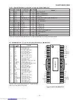
CD-BP1200W/1250W
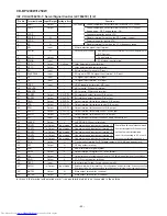
54
P120
T2 PLAY SW_B
Input
PLAY switch for T2
55
P119
FPA
Input
Tape 2 A–Side full proof
56
P118
FPB
Input
Tape 2 B_Side full proof
57
P117
MIC IN
Input
MIC switch
58*
P116
KARAOKE LATCH
Output
Karaoke latch (When not used. Connect to 0V)
59
P115
DISTOUT/SW OUT
Output
Destination output
60
FIP39
SPN
Input
Tuner span change
61*-62*
FIP38-FIP37
NO USE
Input
Open
63*-66*
FIP36-FIP33
P22-P19
Output
FL display driver
67*-70*
FIP32-FIP29
P18-P15
Output
FL display driver
(68*,69)
P103-P100
DIST3-DIST0
Input
Destination input
71-78
FIP28-FIP21
P9-P15
Output
FL display driver
79
VLOAD
VLOAD
––
FL driver (–) power supply.–30V
80-85
FIP20-FIP15
P3-P8
Output
FL display segment
86-89
FIP14-FIP11
P19,12,1,2
Input
Open
90-100
FIP30-FIP0
G9-G1,P17,P18
Output
FL display segment driver
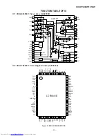
IC701 RH-iX0337AWZZ: System Microcomputer (IX0337AW) (2/2)
Port Name
Terminal Name
Pin No.
Input/Output
In this unit, the terminal with asterisk mark (*) is open terminal which is not connected to the outside.
Function
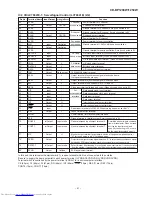
1
TO
CH2 inverted input.
2
FD
CH1 inverted input.
3
FO
CH1 output offset control.
4
FO+
CH1 inverted output.
5
FO-
CH1 non-inverted output.
6
TR+
CH2 inverted output.
7
TR-
CH2 non-inverted output.
8-14
GND
GND
15
SL-
CH3 non-inverted output.
16
SL+
CH3 inverted output.
17
SLDO
CH3 inverted input.
18
VCC1
Power supply 1 (CH1, CH2, CH3)
19
STANDBY
STANDBY signal input.
20
VRFE
CH1-CH4 Reference voltage input.
21
MUTE
Mute signal input (CH6).
22
IN5-
CH5 inverted input.
23
IN5+
CH5 non-inverted input.
24
VCC2
Power supply 2 (CH4).
25
SPO SPDO
CH4 inverted input.
26
SP+
CH4 inverted output.
27
SP-
CH4 non-inverted output.
28
VCC3
Power supply 3 (CH5).
29-35
GND
GND
36*
OUT5+
CH5 non-inverted output.
37*
OUT5-
CH5 inverted output.
38
LOADING M- CH6 non-inverted output.
39
LOADING M+
CH6 inverted output.
40
VCC4
Power supply 4 (CH6).
41
LD_M-
CH6 inverted input.
42
LD_M+
CH6 non-inverted input.
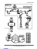
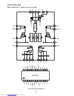
IC3 VHiM63001FP-1: Focus/Tracking/Spin/Sled Driver (M63001FP)
Pin No.
Terminal
Name
Function
1
2
3
4
5
6
7
8
9
10
11
12
13
14
15
16
17
18
19
20
21
28
29
30
31
32
33
34
35
36
37
38
39
40
41
42
27
26
25
24
23
22
TO
FD
FO
FO+
FO–
TR+
TR–
SL–
SL+
SLDO
VCC1
STANDBY
VTEF
MUTE
GND
GND
VCC3
SP–
SP+
SPO SPDO
VCC2(SPN)
IN5+
IN5–
LD_M+
LD_M–
VCC4
LOADING M+
LOADING M–
OUT5–
OUT5+
M63001FP
Figure 43 BLOCK DIAGRAM OF IC
In this unit, the terminal with asterisk mark (*) is open terminal
which is not connected to the outside.
Summary of Contents for CD-BP1200W
Page 46: ...CD BP1200W 1250W 46 M E M O ...
Page 58: ...CD BP1200W 1250W 11 M E M O ...
Page 59: ...CD BP1200W 1250W 12 M E M O ...