– 1 –
CD-BP1450V
No. S7058CDBP145V
CONTENTS
Page
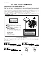
SAFETY PRECAUTION FOR SERVICE MANUAL ........................................................................................................... 2
VOLTAGE SELECTION ..................................................................................................................................................... 2
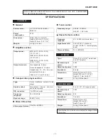
SPECIFICATIONS ............................................................................................................................................................. 3
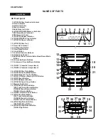
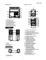
NAMES OF PARTS ........................................................................................................................................................... 4
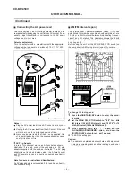
OPERATION MANUAL ...................................................................................................................................................... 6
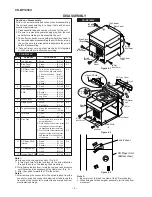
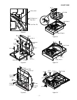
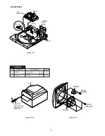
DISASSEMBLY .................................................................................................................................................................. 8
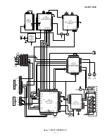
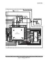
BLOCK DIAGRAM ........................................................................................................................................................... 11
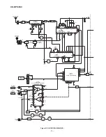
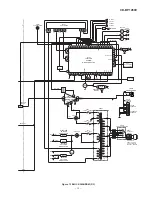
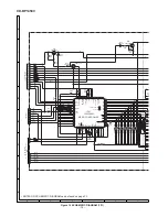
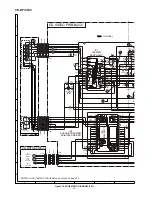
SCHEMATIC DIAGRAM .................................................................................................................................................. 14
WIRING SIDE OF P.W.BOARD ....................................................................................................................................... 25
NOTES ON SCHEMATIC DIAGRAM .............................................................................................................................. 32
TYPES OF TRANSISTOR AND LED ................................................................................................................................ 32
WAVEFORMS OF CD CIRCUIT ...................................................................................................................................... 33
VOLTAGE ........................................................................................................................................................................ 34
REPLACEMENT PARTS LIST/EXPLODED VIEW
• In the interests of user-safety the set should be restored to its
original condition and only parts identical to those specified be
used.
SERVICE MANUAL
This document has been published to be used
for after sales service only.
The contents are subject to change without notice.
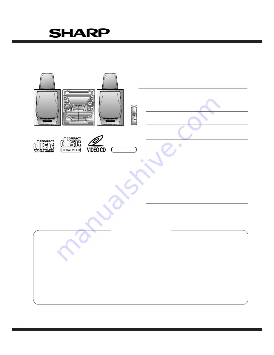
CD-BP1450V Video CD Mini System consisting of
CD-BP1450V (main unit), CP-BK1450 (front speakers)
and GBOXS0043AWM1 (surround speakers).
SHARP CORPORATION
MODEL
CD-BP1450V
VIDEO CD MINI SYSTEM
NTSC/PAL
This Service Manual is for the CD-BP1450V, which is a minor-
modification model of the CD-BP1300V. This manual, therefore,
describes only the changed points from the service manual. Please
refer to the CD-BP1300V service manual (No.S7057CDBP130V)
together with this manual.
CD-BP1300V
Page
REMOVING AND REINSTALLING THE MAIN PARTS .. 11
ADJUSTMENT ................................................................ 12
TROUBLESHOOTING (CD SECTION) .......................... 38
FUNCTION TABLE OF IC .............................................. 42
FL DISPLAY .................................................................... 53
Summary of Contents for CD-BP1450V
Page 47: ...CD BP1450V 12 MEMO ...


