background image

CD-C471 


 M) 

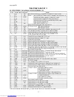
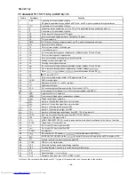
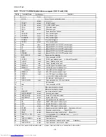
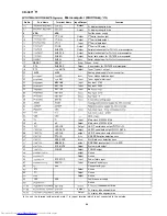
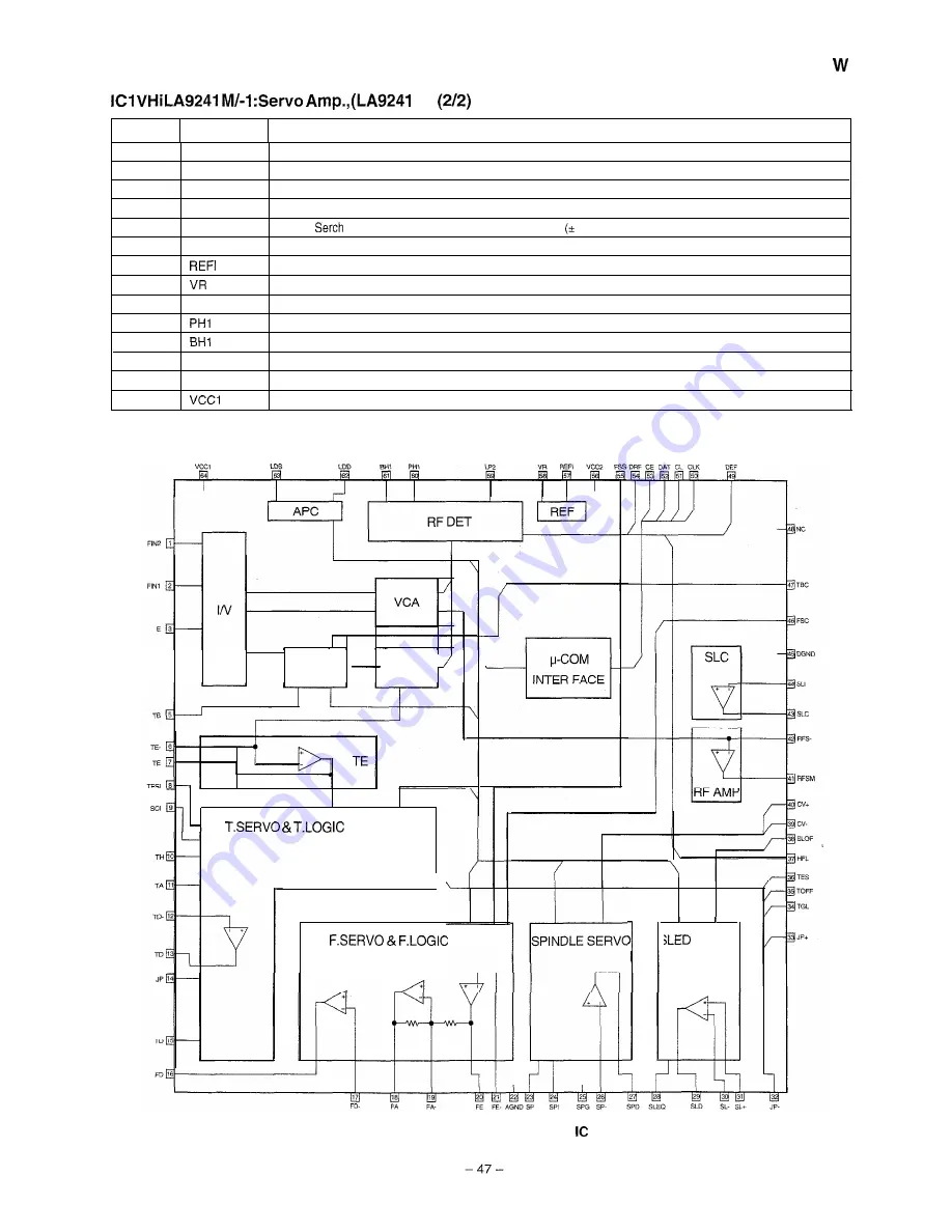
Pin No.

Port Name

Function

51

C L

52

DAT

53

CE

54

DRF

55

FSS

56

vcc2

57

58

59

LF2

60

61

62

LDD

63

LDS

64

Micro computer command clock input pin.

Micro computer command data input pin.

Micro computer command chip enable input pin.

(DETECT RF) RF level detection output.

(Focus 

 Select) Pin to switch focus search mode.    search for reference voltage)

VCC pin for servo system and digital system.

Pin to connect pass control for reference voltage.

Reference voltage output pin.

Pin to set defect detection time constant of disk.

Pin to connect capacitor for peak hold of RF signal.

Pin to connect capacitor for bottom hold of RF signal.

APC circuit output pin.

APC circuit output pin.

RF system VCC pin.

F

E

-

BAL 

 VCA 


SPINDLE SERVC

 SERVC

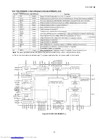
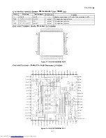
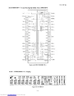
Figure 47 BLOCK DIAGRAM OF 

Summary of Contents for CD-C471 W

Page 1: ...tored to its original condition and only parts identical to those specified be used CONTENTS Page SAFETY PRECAUTION FOR SERVICE MANUAL 2 VOLTAGE SELECTION 2 SPECIFICATIONS 3 NAMES OF PARTS 4 OPERATION MANUAL 6 DISASSEMBLY 7 REMOVING AND REINSTALLING THE MAIN PARTS IO ADJUSTMENT 11 NOTES ON SCHEMATIC DIAGRAM 14 TYPE QF TRANSISTOR AND LED 14 BLOCK DIAGRAM 15 SCHEMATIC DIAGRAM WIRING SIDE OF P W BOAR...

Page 2: ...AUTION Use of controls or adjustments or performance of procedures other than those specified herein may result in hazardous radiation exposure Laser Dkode Properties Material GaAlAs Wavelength 780 nm Emission Duration continuous Laser Output max 0 6 mW CAUTION 0 This Mini Component System is classified as a CLASS 1 LASER product 0 The CLASS 1 LASER PRODUCT label is located on the rear cover l Use...

Page 3: ...D A converter 20 20 000 Hz 90 dB 1 kHz FM 88 108 MHz AM 531 1 602 kHz l Cassette deck section Type Compact cassette tape Frequency response 50 14 000 Hz Normal tape Motor DC motor with electronic governor x 1 Signal noise ratio 55 dB TAPE 1 playback 50 dB TAPE 2 recording playback Bias and erasure system Tape speed Wow and flutter Heads AC 4 76 cmlsec l 718 ips 0 15 WRMS TAPE l Playback x 1 TAPE 2...

Page 4: ...Mode Buttons NORMAL PHANTOM 23 Extra Bass Button X BASS 24 Volume Up Down Buttons 1 7 25 Function Selector Buttons 26 Headphone Socket 27 Clock Button 28 Timer Sleep Button 29 TAPES Record Pause Button l 11 30 CD TAPE Stop Button n 31 Equalizer Selector Demo Mode Button 32 CD Edit Button 33 Tape 1 Edit Button 34 Tuning and Time Up Down Buttons 35 Memory Set Button 36 CD Track Down Review Button u ...

Page 5: ...olby Pro Logic Button 5 Center Mode Button 6 Test Tone Button 7 Balance Control Buttons 0 Tuner control section 8 Preset Up Down Button jA l CD Control section 9 Disc Skip Button 10 Play Repeat Button 4 11 Memory Button 12 Clear Button 13 Pause Button 11 14 Track Down Review Button q f 15 Track Up Cue Button H 16 Stop Button q 17 Random Button 4 I6 llilllllflillillflil llilllilllllllliliil l l 1 I...

Page 6: ...the clock time To change the clock time When the unit is in the stand by mode l When the unit is in the demonstration mode press the DEMO button to enter the clock mode a Press the MEMORY SET button Q Perform steps 6 9 above When the unit is on Press the CLOCK button Q Within 5 seconds press the MEMORY SET button 0 Perlorm steps 6 9 above To see the time display Press the CLOCK button l The time d...

Page 7: ...1 2 Socket D2 xl 1 Screw El xl 8 l 2 Socet E2 xl 1 Screw Fl xl a 2 2 Socket F2 x2 3 Flat Wire F3 x2 4 Tip Wire F4 xl 5 Socket F5 xl 1 Screw Gl x2 8 2 2 Hook G2 x2 1 Screw Hl x12 a 3 1 Open the cassette holder 2 Screw Jl x5 1 Screw Kl x4 2 Socket K2 x2 3 Push Rivet K3 x4 1 Screw Ll xl 2 Cover L2 x4 1 Screw Ml xl 2 Cover M2 xl 1 Screw Nl x2 2 Guide N2 x2 1 Screw Pl x4 a 3 8 4 8 5 8 6 8 6 8 7 1 Screw...

Page 8: ...gure 8 3 Power Kl x4 03 xl 2mm Li xl 03 xlOmm CD Servo PWB Loading Chassis Figure 8 5 M2 xl Washer I Turntable 03 xl Omm Figure 8 6 Qi xl 02 6 xl Omm Be careful when installing the CD changer mechanism Install the CD changer mechanism on the CD player base after the shift lever has been set in the highest position PWB Figure 8 4 Figure 8 7 8 ...

Page 9: ... A5 x2 Tweeter A Front Panel W l Note The center and SURROUND speakers can be easily disas sembled Therefore the disassembling method is not discribed For details refer to the disassembling drawing in the Parts Guide cl Woofer Screwdriver Figure 9 1 Super Tweeter A4 x4 64 xi 4mm AXI I Woofer Figure 9 2 9 ...

Page 10: ...p Down M How to remove the turntable up down motor See Fig IO I 1 Remove the screws Al x 2 PCS to remove the turntable up down motor 02 x5mm Figure 10 l How to remove the pickup See Fig 10 2 1 Remove the screws Bl x 2 PCS to remove the shaft B2 x l pc 2 Remove the stop washer B3 x 1 PC to remove the gear B4 x 1 pc 3 Remove the pickup B2 xl Gear B4 xl Figure 10 2 lO ...

Page 11: ...Setting Instrument Display Adjusting Connection Parts IF 450 kHz 1 602 kHz T351 1 AM Band 531 kHz fL T306 2 Coverage 1 1 0 1 v AM 990 kHz 990kHz fL T302 1 Tracking l Input Antenna Output TP302 2 Input Antenna Output TP301 Notes 1 Description of the FM IF Adjustment is not carried on this Manual It is because the IF coil in the FM front end section has been best adjusted in the factory so that its ...

Page 12: ...he pickup with the or q key VOL Last memory BAL CENTER R GEQ FLAT X BAS OFF Canceling method POWER OFF CD SECTION Figure 12 1 I Since this CD system incorporates the following automatic adjustment function when the pickup is replaced it is not necessary to readjust it Since this CD unit does not need adjustment the combination of PWB and laser pickup unit is not restricted l Automatic adjustment i...

Page 13: ...h The test tone noise is repeatedly output for output period 2 set In this case the following indication appears repeatedly TEST L ch Gch T L S ch t R ch l Pro Logic ON Phantom mode Press the remote control TEST TONE button Output of only L ch tOutput of only R ch I 1 t Output of only S ch The test tone noise is repeatedly output for output period 2 set In this case the following indication appear...

Page 14: ...W SW71 1 TAPE SW712 VIDEO AUX SW718 CENTER MODE PHANTOM SW719 CENTER MODE NORMAL SW721 DOLBY PRO LOGIC BYPASS SW723 REC PAUSE ON E ON E ON m ON E ON CJj J ON m l The indicated voltage in each section is the one measured by Digital Multimeter between such a section and the chas sis with no signal given 1 In the tuner section indicates AM 2 In the main section a tape is being played back 3 in the de...

Page 15: ...NIT ry i t FOCUS COIL TRACKING COIL SKI D MOTOR MOTOR t t t t I PICKUP IN SW4 SLt SL DRF b Bl CNP99 DIGITAL OUT CNPI 1 FM0 SERVO SIGNAL FMIN RES CQCK COIN SQOUT RWC WRQ DAT SELIAL CONTROUCE t OPEN CLOSE CNPIP n ...

Page 16: ... I I Ill I i c r __ __ I Figure 16 BLOCK DIAGRAM 2 3 16 ...

Page 17: ...CD C471 W w UTER lC56115621563 N5M4558L lC562 1 2 Figure 17 BLOCK DIAGRAM 3 3 17 ...

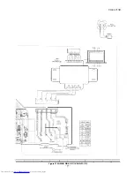
Page 18: ...D PD VR I PICKUP UNIT 0 0 0 2 2 25 2 25 4 7 07 _ I 1 WOTOR PWB3 L CNKq l The numbers 0 to are waveform numbers shown in page 39 l NOTES ON SCHEMATIC DIAGRAM can be found on page 14 1 I 2 I 3 I 4 I 5 I b I Figure 18 SCHEMATIC DIAGRAM l 13 18 ...

Page 19: ...CD C471 W H CD SIGNAL CD DIGITAL OUT 1 JACK PWB A4 L H CD SIGNAL i_cD SERVO PWB C Lj __ _ 7 a 9 10 Figure 19 SCHEMATIC DIAGRAM Z l 3 19 11 12 I ...

Page 20: ...CD C471 W l NOTES ON SCHEMATIC DIAGRAM can be found on page 14 1 2 3 4 5 6 Figure 20 SCHEMATIC DIAGRAM 3 13 20 ...

Page 21: ...CD C471 W L MAIN PWB A1 1 2 w FM SIGNAL _ PLAYBACK SIGNAL RECORD SIGNAL s E H CD SIGNAL cmc 155133 R463 HEADPHONE AMP 9 10 Figure 21 SCHEMATIC DIAGRAM 4 13 2l 11 12 I ...

Page 22: ... c RECRVS v _ A 1 LLL J 1 1 L CH TAPE1 PLAYBACK HEAD I I I RI36 Ic136 1 i 8K 470 106 II 2SC1845 F Q10 5 2SC1845F RECIP 6 RI91 ill I I I h l i l NOTES ON SCHEMATIC DIAGRAM can be found on page 14 1 2 3 4 5 6 Figure 22 SCHEMATIC DIAGRAM 5 l 3 22 ...

Page 23: ...CD C471 W _ r FIN PWB A1 2 I T E 1i i 5 T 18 B KRC104 M SWITCHING 158 Q124 cF KTA1266 GR B SWITCHING R166 RI67 PLAYBACK SIGNAL RECORD SIGNAL 7 8 9 10 11 12 1 Figure 23 SCHEMATIC DIAGRAM 6 13 23 ...

Page 24: ...I1IIIlI I I I II L L I I II I II I I E l I I I I I I I lXOl70AW SYSTEM MICROCOMPUTER C D F I FM SIGNAL I G JK700 HEADPHONES H l NOTES ON SCHEMATIC DIAGRAM can be found on page 14 1 2 3 4 5 6 Figure 24 SCHEMATIC DIAGRAM 7 l 3 24 ...

Page 25: ..._ _ I IT2 R749 IOK I R779 IOK R780 1 AK 4 R761 I 10K I I hhhhhhhhh 18 17 16 15 14 13 1 1 10 EM GZ paggaassa IC702 z lt9g BU2092F OOJOOOOD INPUT OUTPUT EXPANDER R741 IK u LED705 333GTH2 REV I R740 IK LED704 333GTH2 REW R739 1K tu LED703 333GTHP STOP R736 K LED702 333GTH2 FF I R737 1K LED701 T333GTH2 PLAY I 4 FLAT CABLE 263 7 8 9 10 Figure 25 SCHEMATIC DIAGRAM 8 13 25 11 12 I ...

Page 26: ... G H I 901 R905 f I I w o1 I I I I 1 L OF I 8 c 9 KT IIDRR GR r REAR A_GND CENTE CHASSIS GND I c910 b 2200150 I B I i F2 WER PWB B 1 w P p p CHASSIS GND l NOTES ON SCHEMATIC DIAGRAM can be found on page 14 1 2 3 4 5 6 Figure 26 SCHEMATIC DIAGRAM 9 I 3 26 ...

Page 27: ...OTOR 901 EAKER iRMlNAL L W s 1 R CH MIN CENTER 4 OHMS MIN J i I h 0903 IC951 LA4450 POWER AMP HCJN LOFF r f C938 A c941 E 47135 T 0 022 ML C960 I T I CH I 1 FRONT 6 OHMS R CH MIN z w 6 1 2 3 4 5 I a 9 10 11 12 1 Figure 27 SCHEMATIC DIAGRAM 10113 27 ...

Page 28: ... GND FM 750hms VD301 2 KVI 236223F C336 X47OP R324 SE CHASSIS GND CHASSIS GND FE301 FM FRONTEND I I II I I I I I FM SIGNAL 0 AM SIGNAL I B I m w NOTES ON SCHEMATIC DIAGRAM can be found on page 14 1 I 2 3 I 4 I 5 I D I Figure 28 SCHEMATIC DIAGRAM 1 l 13 28 ...

Page 29: ...R354 3 9K t I a I 1 3ov ZD352 R387 3 3 4 MTZJ3 9B 22K KTAI 266 GR Cl361 KRC107 M MPX PHASE D351 n lSS133 ZD351 MTZJ5 1 f m s _ _ B I I n I I I I I II II II II II II II II II I II II L 7 a 9 10 11 12 I Figure 29 SCHEMATIC DIAGRAM 12 13 29 ...

Page 30: ...CD C471 W CD NORMAL REC OTHERCD NORMAL PLAY I 2 I 3 I 4 5 6 Figure 30 SCHEMATIC DIAGRAM 13 l 3 30 ...

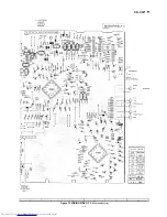
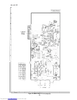
Page 31: ...CD C471 W 1 SWICH PWB A3 1 DISPLAY PWB A2 1 7 8 9 10 11 12 I Figure 31 WIRING SIDE OF P W BOARD l E 3 1 ...

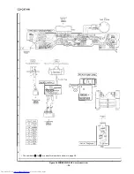
Page 32: ...CD C471 W FLAT CABLE 263 1 24 c CNS12 FWMI 1 MECHANISM P34 1 E TO HEAD PWB P34 2 F G I CNSI 1 E F H TO TUNER PWB P38 2 c 1 2 3 4 5 6 Figure 32 WIRING SIDE OF P W BOARD 2 8 32 ...

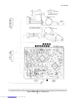
Page 33: ...50 9 FM AM KHz 1100 i 0 SW201 SPAN SELECTOR JK451 Q SUB WOOFER JK452 L CH VIDEO AUX 2 R CH L CH VIDEO AUX 1 R CH 1 WH W 1 WHITE 1 1 BK I BLACK I PK 1 PINK 1 3 TUNER PWB P38 2 c 7 8 9 10 11 12 1 Figure 33 WIRING SIDE OF P W BOARD 3 8 3 3 ...

Page 34: ...9 RECOADiPLAYBACWERACE HEAD 254 8 1 PICKUP UNlT 306 FLAXIBLE PWB HEAD PWB G NSlB CNSlA L CNSPB CNSPA CD DIGITAL OUT r c I _ _ _ JACK PWB A4 1 l The numbers to are waveform numbers shown in page 39 I I 2 I 3 I 4 I 5 I 6 1 Figure 34 WIRING SIDE OF P W BOARD 4 8 34 ...

Page 35: ...CD C471 W CNSIA TTT UP DOWN LOADING CD MOTOR PWB D 1 CNSBA CNSBB DISC MOTOR __ LCNsrli 123 H B TO MAIN PWB P32 1 G x Ei2 7 a 9 10 11 12 1 Figure 35 WIRING SIDE OF P W BOARD 5 8 35 ...

Page 36: ... POWER PWB B 1 MAII IUPWB P33 7 A 1 2 3 4 5 6 Figure 36 WIRING SIDE OF P W BOARD 6 8 36 ...

Page 37: ...CD C471 W TEOl POWER TRANSFORMER M901 FAN MOTOR t I CNS804 I 7 a 9 10 11 12 I Figure 37 WIRING SIDE OF P W BOARD 7 8 37 ...

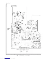
Page 38: ...CD C471 W 1 TUNER PW B H 1 TO pM3A N WB ICNS303j CHASSIE GND FM75 OHMS GND i ANTENNA 2 3 4 5 6 Figure 38 WIRING SIDE OF P W BOARD 8 8 38 ...

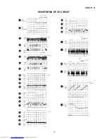
Page 39: ...s 5 0 v TES CUE JP 50ms 10 0 v JP 50ms 0 50 v JP 0 5ms 10 0 JP 0 5ms 10 0 v JP 50ms 10 0 v JP 50lll T 10 0 v JP 50ms 0 50 v JP 50ms 1 00 v TE REVIEW CD C471 W PLAY 20llE l OOV SPO NORMAL DISC TNO Ol cLv 2Oms 2 00 v 6D 50ms 0 1 00 SPO 5Oms 2 00 v CLV 5s IOOmV SLD 0 5s loom SLD I I I i I I I I PLAY TCD 712 140mm TNO Ol 1 i I I i PLAY TCD 712 39 ...

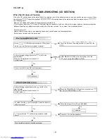
Page 40: ... hand Is from yJ 5 V till OV down pulse approx 300 ms input v Check the SW3 and the wiring from the IC201 pin 54 to the sw3 into the IC201 pin 54 when the turntable is rotating I Yes Is there following voltage input on the IC201 pin 54 in the specific state When the CD mechanism is moved up OV In other states 5V b Check the SW2 MECHA UP SW and the wiring from the No IC201 pin 21 to the SW2 MECHA U...

Page 41: ... pins 3 and 7 during operation stated above No Check the periphery of IC81 OK Yes Check the loading motor M3 and the loading mechanism The CD operating kevs don t work 1 Yes Check the CD DSP power supply and 16 93 MHz clock and reset terminal See if the pick up is in the PICKUP IN SW position 1 Yes If the items mentioned above are OK check the main microcomputer IC701 I Check the Focus HF system P...

Page 42: ...system H i I OV DIV 0 5usec DIV DC When playing back the disc Waveform is unstable Yes Check the spin system 0 5s 1 00 v ICI FD Waveform in case of normal play back 0 55 10 0 v 10 0 v ICI DRF 0 5s 2 00 v ICl TE Figure 42 1 Figure 42 2 l Checkth tiacking system 2 Check waveform of ICl pin 7 TE Check the periphery of lC1 pins 41 and 42 The waveform shown in Fig 42 3 appears and no disc Tracking serv...

Page 43: ...y operation is performed when disc exits Although HF waveform is n Yes Check PDO waveform Fig 43 I Abnormal Check the ICl pins 43 and 44 IC2 pins 3 5 7 10 and 11 1 oo v lC2 PDO 0 5s l OOV IC2 FD j stop Play As VCO freque ncy is locked at ill I I I I I 4 32 M Hz voltage of PDO rises and stabilizes Figure 43 Check IC 2 pin 48 EFLG Usually the number of pulses of flawless disc is 100 pulsesisec or le...

Page 44: ...ection H is output when synchronous signal detected by EFM signal matches synchronous signal internally generated 23 VDD Power terminal of diaital svstem 24 CONTl 25 CONT2 26 CONTB 27 28 29 30 CONT4 CONTS EMPH C2F Input Output General purpose input output terminal 1 Controlled with serial data command input Output General purpose input output terminal 2 from micro computer Input Output General pur...

Page 45: ...inal with asterisk mark is pen terminal which is not connected to the outside 1 Ry M 1 g e n e r a t o r 1 1 1 RAM address FSEQIH Sync detectlon EFM demodulation Interpolation mute Bilingual i I I I I i 4 Digital OUT b DOUT Flag processing of Cl C2 error detection and correction SBE SBSY SFSY CS WRQ SQOUT CQCK 1 bitDAC i_ L P F 57 C2F NC Figure 45 BLOCK DIAGRAM OF IC 45 ...

Page 46: ...al Single end output for CV and CV pin input Spindle amplifier input Pin to connect aain settina resistor in the 12cm mode of soindje I Pin to connect soindte phase comoensation constant toaether with SPD oin I 27 1 SPD I Spindle control sianal output pin I 28 SLEQ I Pin to connect thread phase compensation constant Thread control signal output pin Input pin of thread feed signal from micro comput...

Page 47: ...cus Serch Select Pin to switch focus search mode rt search search for reference voltage VCC pin for servo system and digital system Pin to connect pass control for reference voltage Reference voltage output pin Pin to set defect detection time constant of disk Pin to connect capacitor for peak hold of RF signal Pin to connect capacitor for bottom hold of RF signal APC circuit output pin APC circui...

Page 48: ...AS InDut I 1 kHz BPF soectrum analvzer inout I 27 SPEANA 2 28 SPEANA 1 29 AVDD 30 AVREF 31 TAPE CUM SW 32 ___ 33 vss Input Input Input 4kHz BPF spectrum analyzer input 16kHz BPF spectrum analyzer input A D converter analog positive power A D converter reference power Tape mechanism cam SW input terminal No connected To be connected to GND 34 I Xl I 1 Main clock terminal not used I 35 I x2 I I Main...

Page 49: ...crocomputer IX01 71 AW 2 2 79 TAPE PB EQ output Tape circuit playback Eq selection 80 TAPE REC MUT output Tape circuit record muting output In this unit the terminal with asterisk mark is open terminal which is not connected to the outside 49 ...

Page 50: ...ply for A D converter Tuner station detection input Tuner signal meter input Key input 37 45 Key input 28 36 Kev inout 19 27 1 34 Xl 35 x2 36 P37 37 P36IBUZ 38 P35IPCL 39 P34KI2 Xi x2 LED LCK LED DATA LED CLK RDS ID Input Output Output Output output lnout Main clock 4 194304 MHz Main clock 4 194304 MHz LED IC serial clock output BU2092 LCK LED IC serial data output BU2092 DATA LED IC serial clock ...

Page 51: ...O0 77 PlOO FIPlO GlO 78 80 P97 FIP9 P95 FIP7 G09 GO7 output output output FL display tube segment drive FL display tube grid drive FL display tube grid drive IC601 VHiLC75396N 1 Audio Processor LC75396N Figure 51 I BLOCK DIAGRAM OF IC IC501 VHiLV1035Mkl Dolby Pro Logic Decoder LV1035M LmBPF3 DC OUT3 R_RECT DC OUT4 VLR_TH VCSTH L R_RECT DCOUTP L R RECT D A DC OUT DC OUT L OUT S OUT D GND DET Figure...

Page 52: ...nal to connect capacitor of filter configuration for equalizer F5 band LF2C3 LF2Cl Terminal to connect capacitor of filter configuration for equalizer F2 band In this unit the terminal with asterisk mark is open terminal which is not connected to the outside 52 ...

Page 53: ...GND Standby Gain4 Gain fl Gain1 TX VM4 3 VM4 VM4 3 VM4 GND GND vcc Regbase RegSV 18 19 Reg5V Regbase Figure 54 1 BLOCK DIAGRAM OF IC FL701 VVKBJ549GKb1 FL Display RDS EON Iwl WL Ifi1 L l mUPRO LOGIC S T 4 SP S L E E P CD SRS a kHz ksmss MHz MEMORY d CZ REC q l I q G E3 I q 4k Figure 54 2 FL DISPLAY 53 ...

Page 54: ...CD C471 W MEMO 54 ...

Page 55: ...without lead wire VC l l CY ___ Square type without lead wire VC l l CZ Square type without lead wire VC l l l l l l l l l J The 13th character represents capacity difference J r5 K I O M 20 N 30 2 0 25 pF D 20 5 pF Z 80 20 Resistors VRD _ Carbon film type VRS _ Carbon film type VRN _ _ Metal film type VR l l MF Cylindrical type without lead wire VR l l MN _ Cylindrical type without lead wire VR l...

Page 56: ...ai NPN KRC107 M J AC Silicon NPN KTC3203 Y J AC Silicon PNP KTA1271 Y J AC Digital NPN KRC102 M J AC Silicon NPN 2SC1845 F J AB Silicon NPN KTCSiSS GR J AB Silicon PNP KTA1266 GR J AC Digital NPN KRC104 M J AE Silicon NPN 2SC2878 A J AB Silicon NPN KTC3199 GR J AB Silicon PNP KTAl266 GR J AC Digital NPN KRC104 M J AB Silicon NPN ZSC2236 Y J AC Digital NPN KRC104 M J AB Silicon NPN KTC3199 GR J AB ...

Page 57: ...27 pF 16V AB 2 2 pF 5OV AA 27 pF 5OV AA 0 033 pF 16V AA 0 001 uF 5OV AB 0 1 uF 16V AB 4 7 uF 50V Electrolytic AB 0 1 uF 50V Electrolvtic AA AA AA AA AA AA AA AA AA AA AC AA AA AA A0 AB AA A0 AA AC AA AA A0 AB AA AB AC AA AA AA AA AA AA A0 AA AB AB AB AA AB AA AB AA AB AB AB A0 AC AC AB 0 022 pF 25V 18 pF UJ 5OV 16 pF CH 50V 470 pF SOV 0 022 pF 25V 0 001 pF 5OV 0 022 pF 25V 33 pF 5OV 0 022 pF 25V 0...

Page 58: ... 22 F 50V Electrol ic 22 yF 25V Electrolytic 390 pF SOV 0 022 pF 25V 330 pF lGV Eiectrolytic 0 022 pF 25V 0 001 pF 5OV 0 047 pF 50V Mylar 47 F lGV Electrolytic 220 pF SOV 47 pF 25V Electrolytic 100 pF 5OV 47 pF 25V Electrolytic 0 022 uF 25V 0 001 F 5OV 47 uF 25V Electrolytic 0 022 pF 25V 220 pF lOV Electrolytic 15 pF 5OV 18 DF 5OV o oi F I V 3 3 pF ijOV Electrolvtic VCTYBTlEF223Z J A A 0 022 pF 25...

Page 59: ... J A A 1 kohm l EW J A A 1 kohm ll6W J A A 1 kohm l EW J A A 1 kohm l EW J A A 1 kohm lWW NO R234 235 R237 R238 R240 R241 R242 244 R245 247 R252 R253 254 R256 258 R259 261 R262 R263 R264 R265 R266 R271 R272 R274 R276 R279 R280 R319 R323 R324 R336 R344 R345 R350 R351 R352 R353 R354 R355 R356 R357 R358 R359 R360 R361 362 R363 364 R365 366 R367 R368 R369 R371 374 R376 R377 R378 R379 R380 R381 R382 R3...

Page 60: ...ms l 8W J AA 330 ohms l 6W J AA 33 kohms ll6W J AA 2 2 kohms l 8W J AA 2 2 kohms l bW J J A A a2 ohms l 8W AA 10 kohm l 8W AA 10 kohm l 6W AA 1 kohm l 8W AA 100 ohm l BW AA 1 kohm l 8W AA 100 ohm l GW AA 150 ohms l 8W VRD ST2CDl04J VRD MN2BD104J VRD ST2CD104J VRD ST2CD331 J VRD MN2BD102J VRD ST2CD331 J VRD MN2BDl02J VRD MN2BD102J VRD STZCD102J VRD ST2CD102J VRD MN2BD102J VRD ST2CD333J VRD MN2BDlO2...

Page 61: ...NlZOOAWZZ J AD Connector Ass v ZPin 92LFUSET312E J A D Fuse TS 15A L i5OV 92LFUSE T402 E J A D Fuse TS l5A L 250V 92LFUSE T162 E J A D Fuse T1 6A L 250V 92LFUSE T501 E J A D Fuse T500mA L 2 5 0 V 6 NO PARTS CODE PRICE RANK DESCRIPTION 4 F901 902 FE301 FL701 FW701 FWMI FWM2 JK451 JK452 JK700 Ml M2 M3 92LFUSE T402 E J A D Fuse TS l5A L 2 5 0 V RTUNS0008AWZZ J AN FM Front End VVKBJ549GW 1 J A X F L D...

Page 62: ...ERATION B ButtonOPERATION C CushionLeg NO PARTS CODE y DESCRIPTION 2442 16 HDECQ0369AWSA J AG Display Panel 244 17 JKNBZ0475AWSB J AF Button X Bass 245 QCNWN0769AWZ Z J AD Wire Lug 246 QLUGPOOOlAWZZ J A C L u g 247 QLUGP0002AWZZ J A B LuaTerminal ILua 11 248 QFSHDOOO AWZZ J AB Hoider Fuse 249 92LCAB2781 BSl J AP Side Panel Ass y Left 249 1 Side Panel Left 249 2 Not Replacement Item PCUSG0022AWZZ J...

Page 63: ...cking Add Front Center and Surround Speaker AL Packing Add Rear Center and Surround Speaker AC Polyethylene BagSurround Speaker AB Polyethylene Bag Center Speaker 92L61 OOC471 WOO J Label Feature 92L70032001600 J AC Polyethylene BagFront Speaker 92L71525003200 J AC Sheet Front Speaker 92L72OBPC46200 J AM Packing Add Bottom Front Speaker 92L720TPC46200 92L74231121000 J AM Packing Add Top Front Spea...

Page 64: ...CD C471 w 1 A B C D E F G H I I I I I I I I I I I I I I I I I c 306 I I 306 I I 303 I L I 301 I 1 2 3 4 5 6 CD MECHANISM EXPLODED VIEW 9 ...

Page 65: ...71 W A B C D E F G H __ _ I I I rl 604x37 IlLih 244 244 2w I Y 244 5 ig 267 254 1 254 2 254 3 254 4 254 5 254 6 240 254 7 TAPE MECHANISM 6O x4 616x2 JPWB B 11 _ 619x2 1 2 3 4 5 6 CABINET EXPLODED VIEW l 2 lO ...

Page 66: ...CD C471 W 620 12 614x2 hy2 x b16 226 L 235 234 609x2 611 236 SOLM2 1 2 3 4 5 6 CABINET EXPLODED VIEW 2 2 ll ...

Page 67: ...CD C471 W I WJ 901 I 903x2 I C i I I I 910 I 1 I II JJ 0 ________j__ _ E 907x2 A D F 906x4 4 a 900 G SUPER TWEETER SP5 L CH rn E l 908 H 1 2 3 4 5 6 SPEAKER EXPLODED VIEW l 2 12 ...

Page 68: ...CD C471 W CD C471 W B WOOFER WOOFER SPI SPI 1 1 2 2 3 3 4 4 5 5 6 6 SPEAKER EXPLODED VIEW 2 2 SPEAKER EXPLODED VIEW 2 2 J J 13 13 ...

Page 69: ...CD C471 W WOOFER SPI L CH SP2 R CH SPI 2 904 1 I 2 I 3 I 4 I 5 I 6 SPEAKER EXPLODED VIEW 2 2 14 ...

Page 70: ......

Page 71: ...CD C471 W MEMO ...

Page 72: ...ieval system or transmitted in any form or by any means electronic mechanical photocopying recording or otherwise without prior written permission of the publisher SHARP CORPORATION Communication Systems Group Quality Reliability Control Center Higashihiroshima Hiroshima 739 0192 Japan Printed in Japan A9807 1941SSCS M SA l SZ l EX STL ...

Reviews: