background image


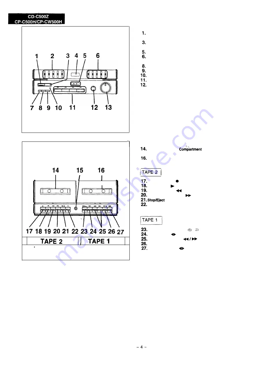
Amplifier section

 Power Switch

2. Graphic Equalizer Controls (LEFT)

 Remote Control Sensor

4. Extra Bass Indicator: X-BASS

 TAPE 1) Direction Indicators

 Graphic Equalizer Controls (RIGHT)

7. Dolby NR Switch

 Tape Selector Switch
 Dubbing Speed Switch

 Power On/Stand-By Indicator
 Function Selector Buttons and Indicators

 Balance Control

1 3. 

Volume Control

Tape control section

 TAPE 2) Cassette 

15. Headphones Socket

 TAPE 1) Cassette Compartment

Record Button:

 Play Button: 
 Rewind Button: 
 Fast Forward Button: 


 Button: 

/r

 Pause Button: II

Reverse Mode Switch: 

Play Button: 
Fast Wind Buttons: 


 Stop/Eject Button: 

,&

Direction Switch: 

Summary of Contents for CD-C500Z

Page 1: ...o those specified be used 1 i INDEX TO CONTENTS Page SPECIFICATIONS 2 NAMESOFPARTS 3 6 VOLTAGE SEl CTION OPERATION MANUAL 6 DISASSEMBLY 2 REMOVING AND REINSTALLING THE MAIN PARTS 13115 CHANGER MECHANISM OPERATION 16 17 ADJUSTMENT 18 21 TROUBLESHOOTING CD SECTION 22 26 FUNCTION TABLE OF IC BLOCK DIAGRAM OF IC 27 33 BLOCKDIAGRAM 34 36 SCHEMATIC DIAGRAM WIRING SIDE OF P W BOARD 37 57 NOTES ON SCHEMAT...

Page 2: ...ntact 3 beam semi conductor laser pickup 200 500 rpm CLV Approx CIRC Cross Interleave Reed Solomon Code 4 times oversampling digital filter and active filter 20 20 000 Hz 95 dB 1 kHz 90 cl6 1 kHz Unmeasurable less than 0 001 W peak Signal readout Rota al speed Error correction Filter Frequency response Signal noise ratio Dynamic range Wow and flutter 0 Cassette deck section Tape A Compact cassette...

Page 3: ...uning Up Down Buttons 13 Memory Button n CD control section 14 Pause Indicator II 15 Play indicator 1 6 Disc Number Indicators 17 Track Number Indicator 18 Minutes and Seconds IndicatoriProgramme Number Indicator 19 Repeat Indicator c 20 Music Schedule Over Indicator 21 Music Schedule Indicators 22 Programme Indicator 23 Random Play Indicator 24 Disc Number Select Buttons 25 Magazine Compartment 2...

Page 4: ... 8 Tape Selector Switch 9 Dubbing Speed Switch 10 Power On Stand By Indicator Il Function Selector Buttons and Indicators 12 Balance Control 1 3 Volume Control n Tape control section 14 TAPE 2 Cassette Co artment 15 Headphones Socket 16 TAPE 1 Cassette Compartment 17 Record Button 0 18 Play Button b 19 Rewind Button U 20 Fast Forward Button H 21 StoplEject Button n r 22 Pause Button II 23 Reverse ...

Page 5: ...om Play Sutton 1 9 Memory Button 20 Clear Button q Proper use of the remote control Aim the remote control at the remote control sensor with 60 with no obstacles and operate as shown Notes concsrnlng uss 0 Replace the batteries if control distance decreases or operation becomes erratic l Periodically clean the transmitter wlndow on the rsrnote control and the sensor on the main unit with a soft cl...

Page 6: ...m 3 1 2 n APSS Auto Program Search System 5 1 2 3 n APMS Automatic Programmable Music Selector ...

Page 7: ...P AY REPEPlT 1 ...

Page 8: ...e off nylon bands or wire holders where they need be removed when disassembling the unit After servicing the unit be sure to rearrange the leads where they were before disassembling 4 Takesufficientcareonstaticelectricityoftntegratedcircuits and other circuits when servicing Figure 12 1 msp ay PWS Figure 12 2 4 Back Board 1 screw Dl X 5 11 Z 5 CD Block 1 screw El x 4 11 3 2 Socket EP x 3 Figure 1 ...

Page 9: ...ove the drive belt 2 Remove the washers Cl C3 and the stop wasper C2 with a small precision screwdriver to extract the flywheel from the chassis How to remove the flywheel of tape 2 side See Fig 1 3 2 and 13 3 1 Remove the drive belt 2 Remove the screws 83 x 2 PCS and remove the motor fixture 3 Remove the stop washer C4 with a small precision screw driver to extract the flywheel from the chassis N...

Page 10: ... ascertain that it runs at DC 1 5V or less CD CHANGER MECHANISM SECTION Removing the CD changer motor See Figs 15 3 and 15 4 1 Before remowng the motor mounting chassis turn the load gear and lift gear in the direction of the arrow as far as it will go 2 Remove the 3 chassis screws Al which hold the loading motor and lift motor 3 Removethe other 2 screws A2 which hold the loading motor and remove ...

Page 11: ...________ ___ __ __ __ __ __ ____________________ __ _ _ Play hlOadln6 Loading StoP UnloadIns 4th DISC LoadIns Figure 17 l Time Chart Llft M o t o r U P D o w n DISC I SWSM Photo Jnterruptsr LoadIns h0TOR Close 7 la tv0TOR3 40mS UnloadIns ComPlsta Lift Motor Down Complete LoadlnG Complete UnloadInS ComPiete Lift Motor UP ComPlete Loading ComPiste Figure 17 2 17 ...

Page 12: ...en performing the high speed adjustment TAPE SECTION L Position of each switch or control Volume Max Graphic Equalizer Center Function Tape Dolby NR Off Beat cancel A Tape selector Normal Dubbing speed Normal l Bias Frequency Adjusting Specified Value Instrument Point Connection L411 100 kHz Q421 Emitter BEAT CANCEL Switch A l Bias Current 1 Adjusting Point Specified Value Instrument Connection L ...

Page 13: ...ut Antenna Output Pin 15 of IC202 Output Collector of Q216 3 input Antenna Output Collector of 0214 i l F M IF RF Signal generator 1 kHz 40 kHz dev FM modulated Test Stage Frequency Frequency Setting Instrument Display Adjusting Connection Point Band 67 5 MHz 1324 fL l l coverage 1 a5 v i 50 mV RF 98 00 MHz 98 00 MHz T321 ST322 l 2 1 O 30 dB IF 98 00 MHz 98 00 MHz 2 1 O 30 dB l Input Antenna 0utpu...

Page 14: ...djusting Adjusting Method Instrument Connection Point VR4 l 1 TPl TGl and GND 1 Short circuit the Pin 4 of IC4 and GND Adjust so as to obtain symmetric waveform Figure 20 2 when DC is 0 V l Focus Gain 2 Apply sine wave Oscillation Frequency 1 O kHz 1 O Vrms as shown in Figure 20 3 l Tracking Gain Adjusting Adjusting Method Instrument Connection Point VR5 Adjust so that the TPl TGl TG2 voltage of C...

Page 15: ... GENERATOR I I 470 i TRACKING GAIN ADJ JIG i I I I I I 0 11 1 Figure 21 1 TRACKING GAIN Figure 21 2 HF OUTPUT ICI 1 I 3 7 TGI TG2 HF FG2 FGI GND PI VRI EEl JjL GE VR2 t 1 65 2 IV P P 25 IEF I i I Figure 21 3 ADJUSTMENT POINTS 21 ...

Page 16: ...ircuit voltage I I i 1 i Is the oscillating circuit XL801 of the control microcomputer IC801 operating normally Yes Check the XL801 and peripheral circuits and replace No faulty parts Check to see that the reset circuit of the control microcomputer IC801 is operating normally Normal 1 Defectivec Check the reset circuit lC802 and peripheral circuits and I replace faulty parts I Is the drive signal ...

Page 17: ...fn to the power supply is damaged control microcomputer IC801 The disc 1 switch is defective Replace it Is the photo interrupter signal H being input to pin 47 of p Replace the photo interrupter the control microcomputer IC801 No Yes Is the motor drive output being output from pins 43 and 45 of the control microcomputer IC801 No The control microcomputer IC801 is defective Replace it Yes Is the mo...

Page 18: ...gram Is the tracking error signal pin 2 of IC2 being output ____ No No m Is the tracking signal being output I I I from the oickuo main unit I I I Yes Yes rF lace the 1 In the stop mode is the tracking coil drive output pin 4 of 7 Incorrect adjustment 1 CNPP 0 SOmV In the stop mode adjust the tracking offset to 0 I 50mV j Yes Is the tracking coil drive output being output from the tracking driver ...

Page 19: ...a high level I i Yes Is the high low level repetition output for leading the focus servo yICl is defective No Yes Yes No i Yes Is the output of pin 31 of IC2 as shown below _ _ Pin 69 of ICI FRF Pin 31 of IC2 FE Yes Is the high low repetition output Check to see thit the focus circuit is normal and check being output from pin 8 of IC4 the distribution connector 1 The pickup is defective Replace it...

Page 20: ...f the slide motor driver IC5 Normal The slide motor driver lC5 is defective Repace it Check if there is voltage at CNP3 CNSS and Ml Is there audio output No Is there audio output from both L and R channels Yes e l Check the muting Transistor Q6 and Q8 and replace No l Check the sound coupling capacitors Cl5 L CH andClG R CH 1 Is there 5V at IC9 Yes hi Check power circuits ICI2 and IC13 N o r Is pi...

Page 21: ...L3 56 VL2 57 VLl 56 61 COMO 3 62 80 SEGO 18 operation is confirmed when disc Input Detects whether a magazine is locked or not With magazine locked L Input The voltage of VL3 are applied to the LCD Input The voltage of VL2 are applied to the LCD Input The voltage of VLl are applied to the LCD Output LCD common output terminal Output LCD segment output terminal In this unit the terminal with asteri...

Page 22: ...pply Output Crystal clock synchronizing signal 30 DROM detection flag CD ROM terminal al obcillation clock 6 4672 Input for applying the trackin In this unit the terminal with asterisked mark is open terminal which is not connected to the outside 28 ...

Page 23: ...P KP HF TEF SVOF TRBI FEM Z DATA DS I TO TQ SDO SD 2 DTFL SD1 r r I NTERFACE CLOCK CIRCUIT EFM DEMODULATOR SiGNAL BUFFER b 4 DET CORRECT 16K RAM r c I 4 DATA CONTROL DIGITAL FILTER D A L UUIWI 1 1 CDROM I 8 DGL DGR LJR WDCK t DFOO t DFOI DEP Figure 29 BLOCK DIAGRAM OF IC 29 ...

Page 24: ...Non connection 6 1 SEG8 6 2 SEG9 6 3 SEGlO 6 4 SEGll 65 SEG12 output LCD segment output terminal output LCD segment output terminal output LCD segment output terminal output LCD segment output terminal output LCD segment output terminal 6 6 SEGl3 O u t p u t 67 SEG14 Output LCD segment output terminal LCD segment output terminal In this unit the terminal with asterisked mark open terminal which is...

Page 25: ...1846AFZZ lX1846AF POWER VDI VS VLC LCD DRIL POWER HOLD INPUl RESET I NPUl TESl XIN XOUl r LCD CONTROL DRIVER TIMING GENERATOR TIMER a HIGHT 4 CLOCK WATCH w LOW GENERATOR DOG TIMER Figure 31 BLOCK DIAGRAM OF IC 31 ...

Page 26: ...IC805 92LiC ix1874 RH IXl874AF 71 i onnect the ceramic Tuner preset down In this unit the terminal with asterisked mark is open terminal which is not connected to the outside 32 ...

Page 27: ...IC2 VHiLA9200Mbl LA9200M i v 6ZK II I 5 1 2vcc i L FIV2 wcJ FOCS VEE VRI VR2 rc l t o 6V I I EO y TES TOFF JP Figure 33 BLOCK DIAGRAM OF IC 33 ...

Page 28: ...7 3 I I rt Figure 34 BLOCK DIAGRAM l 2 34 ...

Page 29: ... L ...

Page 30: ...I ...

Page 31: ......

Page 32: ...x iii S I 1 ...

Page 33: ...A B C D E F G H I ...

Page 34: ... IL ...

Page 35: ......

Page 36: ...I e I I ...

Page 37: ...I 5 Y i Y b I a I m 0 I I 1 cl w Y I3 I ...

Page 38: ... I ...

Page 39: ... a m I 0 I a w u cl I I ...

Page 40: ... a symbol P is used this sym bol P means micro micro farad and the unit of the capacitor without such a symbol is microfarad As to electrolytic capa citor the expression capacitance withstand voltage is used CH TH RH UJ Temperature compensation ML Mylar type P P Polypropylene type The indicated voltage in each section is the one measured by Digital Multimeter betweensuchasectionandthechassis with ...

Page 41: ... 2SB562 C 2SA970 BL 92LCZRD 1318B D S G 2SK544 F B C E 2SD 1764 B C E 2SD2061 E 2SB1185 E 258 1287 KV1236Z23F SLR34YC3F SLR54W3F RD52 4A Figure 59 1 TYPES OF TRANSISTOR AND LED 92LCtIRD 1393A 92LCsRD 1387A 9ZLPLUG155A Figure 59 2 AC POWER SUPPLY CORD AND AC PLUG ADAPTOR 59 92LPLUG027 1 T 2 r 3 I 4 1 5 16 Figure 60 TAPE MECHANISM EXPLODED VIEW 60 ...

Page 42: ...3 0 2 I 1 1 2 r I 3 4 r Figure 61 CD MECHANISM 5 EXPLODED 6 VIEW I 61 G 62 ...

Page 43: ...A B C D E F G H 3 4 Figure 63 CABINET EXPLODED VIEW 112 63 64 ...

Page 44: ...8 ...

Page 45: ...6 Q957 Q95B 4959 Q960 Q981 Q982 Q983 Q984 Q985 Q986 Dl 6 D13 16 D204 0205 0206 207 D208 D209 D210 D211 D213 D214 D215 216 D217 220 D221 D222 D401 405 D406 412 0415 423 0425 430 D431 D432 433 D591 594 D595 596 D599 D601 602 D603 604 0752 DBOl 808 D809 D811 0817 820 D822 826 D901 902 0903 D951 PART NO DESCRIPTION VSDTCl14YS 1 J Digital NPN DTClld YS VSDTAll4YS 1 J Di l PNP DTA114 YS VSDTAlI4ES 1 J D...

Page 46: ...IHHZPQJ J 22 pF CH SOV RCmGZAIQ4AFIH J 0 1 F SOV Electrolybc RC GZAIQ7AFlC J 100 F l6V Electrolytic VCFYSAlJA104J J 0 1 flF SOV Thm Film VCCSMNIHL68QJ J 68 pF SOV VCCSMNlHL2703 J 27 pF SOV VCFYSAlJAlQlJ J 0 1 pF 63V Thin Film RC GZA227AFOJ J 220 pF 6 3V Electrolytic RC GZA225AFIH J 2 2 pF SOV Electrolytic VCKYMNLHBLQZK J 0 001 F SOV VCTYPAlCX104J J 0 1 pF 16V VCTYMNlCY123M J 0 012 pF 16V RC GZA335...

Page 47: ... A A A B A A A A A A A B A B A B A A A B A B A B A B A B A B A B A A A A A A A B A A A A A A A B A A A B A B A A A B A B A B A A A A A B A A A B A B A A A B A A c703 704 C705 706 C707 708 c709 c710 C711 712 c713 714 C715 716 C717 JB c719 720 C721 722 C723 724 C725 726 C727 728 c729 730 C731 732 c751 C752 c753 c754 c755 C756 757 caoi 804 cao7 C809 810 cai3 cai4 ca15 C816 cai9 821 ca23 a27 ca29 830 ...

Page 48: ...A A A A A A A A A A A A A A A A A A A A A A A A A A A A A A A A A A A A A A A A A A A A A A A A A A A A A A A A A A A A A A REF NO PART NO R77 R78 R79 R80 81 R82 R83 R84 R85 R86 R87 R88 R89 R90 92 R93 R94 R96 100 RlOl 103 R104 R105 R106 R107 R108 R109 llO Rlll R112 R113 R114 R115 R117 R118 R119 R121 R122 RI23 R124 R125 126 R127 RI28 R129 R130 R131 R132 R133 R134 R135 R136 R137 R138 R139 140 R141 R...

Page 49: ... A A A A A A A A A A A A A A A A A A A A A A A A A A A A A A A A A A A A A A A A A A A A A A R307 R308 R309 R310 R321 R322 R323 R324 R325 R326 R327 R328 R329 R330 R331 R332 R333 R334 R335 R336 R401 R402 R403 R404 R405 R406 R407 R408 409 R410 R411 R412 R413 R414 R415 416 R418 R419 R420 R421 R422 R423 424 R425 426 R427 R428 R429 430 R431 432 R433 434 R435 436 R437 438 R439 R443 446 R447 449 R450 R45...

Page 50: ... A A A A A A A A A A A A A A A A A A A A A A A A A A A A A A A A A A A A A A A A A A A A A A A A A A A A A A A A A A A A A A A A A R679 680 R687 688 R693 R695 R696 R697 R698 R699 R701 702 R703 704 R705 706 R707 708 R709 710 R711 712 R713 714 R715 716 R717 718 R719 720 R721 722 R723 724 R725 726 R727 728 R729 730 R731 732 R733 734 R735 736 R737 738 R739 740 R751 752 R753 R755 756 R771 772 R773 774 ...

Page 51: ...A A A A A A A A A A A A A A A A A A A B A C A B A A A B A C 7 5 CNP6 CNP8 CNP201 CNP401 CNP402 CNP403 CNP404 CNP451 CNP452 CNP501 CNP601 CNP651 CNP701 CNP751 CNP801 CNP901 CNP902 CNP903 CNP951 CNP972 CNSlA B CNSPA B CNS3 Bl3 CNS4 CNS8 Bl8 CNS9 Bl9 CNSPOl CNS401 CNS402 CNS403 CNS404 CNS451 CNS501 Bl501 CNS601 CNS751 51751 CNS801 CNS803A B CNS901 Bl901A B CNS902 Bl902 CNS903 Bl903 CNS951 Bl951 CNS97...

Page 52: ...4R19211423 6 94R19211424 7 94R19211425 8 94R19211466 9 94R19211461 10 94R19211413A 11 94R19211455 12 94R19211412 13 94R19211411 14 94R19211414 15 94R192101501 16 94R19211416 17 94R19211417 18 94R19210204 19 94R19211464 20 94R19211420 21 94R19211421 22 94R19211415 25 94R19210314 27 94R19210306 28 94R18210308 29 94R19210303 30 94R19211418A 34 94R18210307 35 94R192104312 37 94R19212604A 38 94R1921073...

Page 53: ... U A L A A A H A C A A A E A E A C A C A C A C A A A A A A A H A D A A A B A H A A A A A G A A A G A N A N A B A C A C A C A D A A A 0 A C A A A C A A A C A P A A A D A F A A A D A F A C A A A B A F A H e e e 395 398 393 400 401 402 404 405 415 416 417 418 419 421 423 424 425 426 427 428 429 430 431 432 433 434 435 436 437 438 CNS401 M401 M402 SW451 94R185110501 94R18213107 94R18293103 94Rl8513101...

Page 54: ...A A A A A A A A A A A A A B A C A D A C A F A C A A A A A A A A A A A A A A A A A A A P A P A Z A D A H A C A C A A A B A B A B A E A E A D A A REF NO 407 PART NO DESCRIPTION CODE LBSHC0004AGZZ J Bushing AC Power Supply A B Cord 408 92LCCoV1587ASl J Tl Cassette Cover Ass y A K 1408 l Cassette Cover Not 408 2 409 Replacement Item 92LPANEL1587B J PaneLCassette C o v e r A C 92LCCoV1587BSl J T2 Casse...

Page 55: ...sher 4mm 92L3BTSt12BZ J Screw d3X 12mm ACCESSORIES PACKING PARTS GCASPO 118AFSA J Magazine Unit JHNDP 1114AFZZ J Handle Carton QANTL AFZZ J Loop Antenna 92LBAG1460B J Polyethylene Bag Accessories 92LBAG1585A J Polyethylene BagUnit 92LBAG760C J Polyethylene Bag AC Plug Adaptor For Saudi Arabia 92LF ANT1533A J FM Antenna 92LG CARD1266A J Warranty Card For Australia and New Zealand 92LiNST1586A J Ope...

Page 56: ...50C500 J PadCenter 92L1024cw500 J Polyethylene BagSpeaker A C A X A C A D A D A G A A A A A B A B A C B A A R A R A F A H A F A C A F REF NO PART NO t DESCRIPTION 901 902 903 904 905 906 907 908 909 910 911 912 913 SP10 1 92L1001cw500 92L1002CW500H 92L1008CS 500H 92L1009cw500 92L10100v500 92L1011Cw500 9211012C 500H 9211014cw500 92L1015CvV500H 92L1017CvV500 92LOO602CP x9 92L1018cW500 9211019cw500 1...

Reviews: