– 61 –
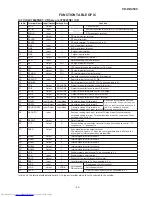
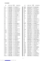
CD-DD4500
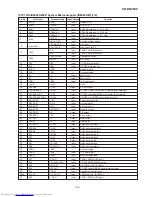
1
SDOS
Input
SDTO source select pin. (Note 1)
“L”: internal ADC output, “H”: I2C DAUX input
2
I2C
Input
Serial control mode select pin. “L”: 3-wire serial, “H”: I2C bus
3
SMUTE
Input
Software mute pin. (Note 1)
Software mute is started with “H” and canceled with “L”.
4
BICK
Input
Audio serial data clock pin.
5
LRCK
Input
Input channel clock pin.
6
SDTI1
Input
DAC1 audio serial data input pin.
7
SDTI2
Input
DAC2 audio serial data input pin.
8
SDTI3
Input
DAC3 audio serial data input pin.
9
SDTO
Output
Audio serial data output pin.
10
DAUX
Input
Auxiliary audio serial data input pin.
11
DFS
Input
Double-speed sampling mode pin. (Note 1)
“L”: normal speed, “H”: double speed
12*
N.C.
—
Not connect.
13
DZFE
Input
Zero input detection function enable pin.
“L”: mode 7 (disable) in parallel mode, selectable with DZFM2-0 bit in serial mode.
“H”: mode 0 (output from DZF1 with AND of 6 ch)
14
TVDD
Input
Power supply pin for output buffer, 2.7 V - 5.5 V.
15
DVDD
Input
Digital power supply pin, 4.5 V - 5.5 V.
16
DVSS
—
Digital ground pin, 0 V.
17
PDN
Input
Power down & reset pin. When this pin is switched to “L”, it enters the power down state
and the register is initialized. Reset it with the PDN pin if P/S and CAD0-1 are changed.
18
TST
Input
Test pin. Connect it to DVSS.
19*
N.C.
—
Not connect.
20
ADIF
Input
Analog input type select pin. “H”: differential input, “L”: single end input
21
CAD1
Input
Chip address 1 pin.
22
CAD0
Input
Chip address 0 pin.
23
LOUT3
Output
DAC3 L channel analog output pin.
24
ROUT3
Output
DAC3 R channel analog output pin.
25
LOUT2
Output
DAC2 L channel analog output pin.
26
ROUT2
Output
DAC2 R channel analog output pin.
27
LOUT1
Output
DAC1 L channel analog output pin.
28
ROUT1
Output
DAC1 R channel analog output pin.
29
LIN-
Input
L channel analog inversion input pin.
30
LIN+
Input
L channel analog non-inversion pin.
31
RIN-
Input
R channel analog inversion input pin.
32
RIN+
Input
R channel analog non-inversion pin.
33*
DZF2
Output
Zero input detection 2 pin. (Note 2)
If the group 2 input data has been “0” for 8,192 consecutive times or the RSTN bit is “0”, it
changes to “H”.
OVF
Output
Analog input overflow detection pin. (Note 3)
It changes to “H” when the analog input to L-ch or R-ch overflows.
34
VCOM
Output
Common voltage output pin, AVDD/2
Mount a capacitor of large capacity (approx. 2.2
µ
F) to remove power source noise.
35
VREFH
Input
Reference voltage input pin, AVDD.
36
AVDD
Input
Analog power supply pin, 4.5 V - 5.5 V.
37
AVSS
—
Analog ground pin, 0 V.
38*
DZF1
Output
Zero input detection 1 pin. (Note 2)
If the group 1 input data has been “0” for 8,192 consecutive times or the RSTN bit is “0”, it
changes to “H”.
39*
MCLK
Input
Master clock input pin.
40
P/S
Input
Parallel/serial select pin.
“L”: serial control mode, “H”: parallel control mode
IC505 RH-iX0454AWZZ: 6-CH CODEC IC (AK4527BVQ) (1/2)
Terminal Name
Pin No.
Input/Output
Function
In this unit, the terminal with asterisk mark (*) is (open) terminal which is not connected to the outside.
Summary of Contents for CD-DD4500
Page 70: ...CD DD4500 70 MEMO ...
Page 87: ...CD DD4500 16 MEMO ...

