CD-G10000/CP-G10000S
8 – 9
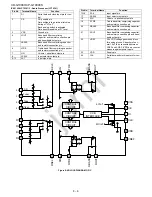
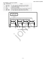
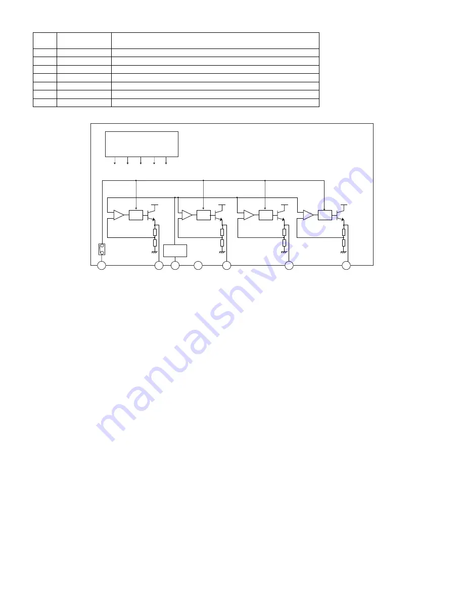
IC851 VHIAN80T53/-1: Multi Regulator (AN80T53)
Pin
No.
Terminal Name
Function
1
REG4 Output
5.1 V power supply with a minimum peak out current of 1200 mA.
2
REG3 Output
13 V power supply with a minimum peak out current of 1350 mA.
3
VCC
Connected to Power supplies.
4
GND
Connected to the IC substrate.
5
MODE 1
REG1, REG2,REG3 and REG4 outputs are turned ON when this pin is 5 V.
6
REG2 Output
10 V power supply with a minimum peak out current of 800 mA.
7
REG1 Output
8.5 V power supply with a minimum peak out current of 700 mA.
5
2
3
4
1
7
6
Peak Current Protection,
Thermal Protection,
Load Short Protection.
Out puts
-
+
-
+
Prc
Drive
-
+
Prc
Drive
-
+
Prc
Drive
Prc
Drive
Reference
Voltage
MODE1
REG3
13V
REG4
5.1V
REG1
8.5V
REG2
10.0V
VCC
GND
Figure 8-9 BLOCK DIAGRAM OF IC
jomi
Summary of Contents for CD-G10000
Page 16: ...CD G10000 CP G10000S 2 11 CHANGE COLOR TO BLACK 150 151 148 7 j o m i ...
Page 19: ...CD G10000 CP G10000S 2 14 10 148 147 146 145 j o m i ...
Page 29: ...CD G10000 CP G10000S 2 24 BIG SLOT FACING OUT 110 20 j o m i ...
Page 33: ...CD G10000 CP G10000S 2 28 804 24 SCREW TORQUE 3 kgf cm 0 5 0 j o m i ...
Page 41: ...CD G10000 CP G10000S 2 36 NO GAP HAVE GAP O K N G 32 j o m i ...
Page 49: ...CD G10000 CP G10000S 3 8 MEMO j o m i ...
Page 59: ...CD G10000 CP G10000S 5 4 M E M O j o m i ...
Page 126: ...CD G10000 CP G10000S 30 j o m i ...
Page 137: ...CD G10000 CP G10000S MEMO 11 j o m i ...

