background image

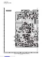
CD-SW440N

6 – 25

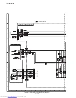
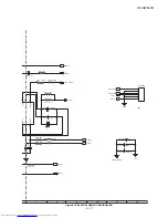
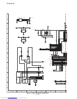
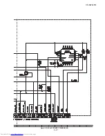
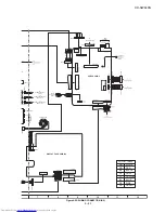
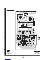
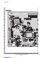
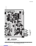
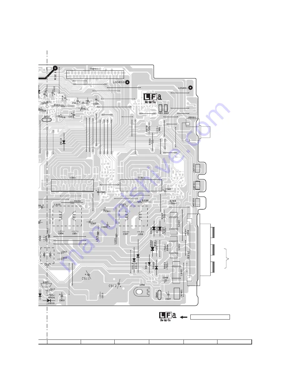
Figure 6-24: WIRING SIDE OF MAIN PWB (TOP VIEW) (2/2)

B

C

E

EC

B

2

4

6

8

10

12

14

16

1

3

5

7

9

11

13

15

18

20

22

24

17

19

21

23

26

28

30

25

27

29

32

31

33

VIDEO OUT

SUBWOOFER LIGHT-UP

FRONT SPEAKER LIGHT-UP (R-CH)

FRONT SPEAKER LIGHT-UP (L-CH)

SUBWOOFER OUTPUT

1

2

1

2

1

2

1 3 5 7 9 11 13 15 17 19 21 23

2 4 6 8 10 12 14 16 18 22

1 3 5 7 9 11 13 15 17 19 21 23

2 4 6 8 10 12 14 16 18 22

2

1

R-CH

FRONT SPEAKERS

TERMINAL

L-CH

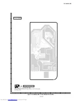
Lead-free solder indication

Lead-free solder is used in the MAIN PWB.
Refer to "Precautions for handling lead-free solder" for instructions 
and precautions.

7

8

9

10

11

12

Summary of Contents for CD-SW440N

Page 1: ...rts Of Connecting Wires 6 22 5 Wiring Side Of PWB 6 24 CHAPTER 7 FLOWCHART 1 Troubleshooting 7 1 CHAPTER 8 OTHERS 1 Function Table Of IC 8 1 2 FL Display 8 9 PARTS GUIDE MINI COMPONENT SYSTEM CD SW440N MODEL CD SW440N Mini Component System consisting of CD SW440N main unit CP S440N speaker system and CP SW440N subwoofer CONTENTS SHARP CORPORATION Parts marked with are important for maintaining the...

Page 2: ...d free solder Sn Ag Cu is about 220 C which is higher than the conventional lead solder by 40 C and as it has poor solder wettability you may be apt to keep the soldering bit in contact with the PWB for extended period of time However since the land may be peeled of for the maximum heat resistance temperature of parts may be exceeded remove the bit from the PWB as soon as you confirm the steady so...

Page 3: ...URER UNE LONGUE PROTECTION CONTRE UN INCENDIE REMPLACER SEULEMENT PAR UN FUSIBLE DE F801 F802 6A 125V F803 F804 2A 125V F805 5A 125V F808 1 6A 125V FUSES Before returning the audio product to the user perform the following safety checks 1 Inspect all lead dress to make certain that leads are not pinched or that hardware is not lodged between the chassis and other metal parts in the audio product 2...

Page 4: ...ck Frequency response 50 14 000 Hz normal tape Signal noise ratio 50 dB playback Wow and flutter 0 35 WRMS USB USB host interface Complies with USB 1 1 Full Speed 2 0 Mass Storage Class Support Bulk only and CBI protocol Support file MPEG 1 Layer 3 WMA Non DRM Bitrate support MP3 32 320 kbps WMA 64 160 kbps Other Maximum total number of MP3 WMA files is 1024 Maximum total number of folders is 255 ...

Page 5: ... WMA Total Indicator 8 Daily Timer Play Indicator 9 FM Stereo Mode Indicator 10 FM Stereo Receiving Indicator 11 Tape play Indicator 12 Memory Indicator 13 Extra Bass Indicator 14 Disc USB Repeat Play Indicator 15 Disc USB Pause Indicator 16 Disc USB Play Indicator FUNCTION FUNCTION AUDIOIN AUDIOIN PHONES PHONES VOL VOL POWER POWER ON STAND BY ON STAND BY MINI COMPONENT SYSTEM CD DH790 PUSH PUSH O...

Page 6: ...uning Down iPod Cursor Down Button 17 Demo Button 18 iPod Button 19 Disc Button 20 USB Button 21 Audio In Button 22 Open Close Button 23 iPod Menu Button 24 iPod Play Pause Button 25 Disc USB Play Pause Button 26 X Bass Button 27 Equaliser Mode Button 28 Clock Timer Button 29 Sleep Button 30 Tuner Preset Up Button 31 CD Track Up or Fast Forward Time Up Button 32 Tuner Preset Down Button 33 Tape Bu...

Page 7: ...er Specified Value Play TW 2111 Tape 1 Over 90 g Torque Meter Specified Value Play TW 2111 29 to 75 g cm Fast Forward TW 2231 55 to 170 g cm Rewind TW 2231 55 to 170 g cm Test Tape Adjusting Point Specified Value Instrument Connection Normal speed MTT 111 Variable Resistor in motor 3 000 90 Hz Speaker Speaker Terminal Load resistance 6 ohms Tape Motor Variable Resistor in motor TAPE MECHANISM ...

Page 8: ... PWB E2 x 1 D2 x 2 G2 x 1 Front Panel Hook E1 x 1 Hook E1 x 1 G3 x 1 F1 x 9 M3 x 10mm B1 x 2 M3 x 10mm B1 x 2 M3 x 10mm B1 x 2 M3 x 10mm A1 x 1 M3 x 12mm A1 x 2 M3 x 12mm B1 x 2 M3 x 10mm A1 x 2 M3 x 12mm Side Panel Left Side Panel Right H1 x 1 Special Screw H1 x 1 Special Screw PULL PULL Power PWB Rear Panel Front Panel Top Cabinet Rear Panel Fan Motor Main PWB Lug wire A2 x 1 iPod PWB STEP REMOV...

Page 9: ...mm M4 x 4 M2 6 x 10mm H1 x 2 M3 x 6mm G3 x 1 G3 x 2 G2 x 1 Front Panel Front Panel Front Panel Audio In PWB L1 x 1 Special Screw Q1 x 4 Special P2 x 1 Display PWB Tape Mechanism Lug wire Display PWB Hook G4 x 1 Hook G4 x 1 PULL PULL Figure 4 Figure 5 Figure 6 Figure 9 Figure 8 Figure 7 CD Mechanism Changer Mechanism Unit Changer Mechanism Unit Changer Mechanism Unit ...

Page 10: ...ter TO LED PWB Speaker Box Woofer LED PWB E R U G I F P E T S Front Panel Assy 1 1 A1 X1 10 2 Socket A2 X1 3 Screw A3 X2 2 Woofer 1 Screw B1 X4 10 3 Tweeter 1 Screw C1 X2 10 PROCEDURE CP S440N LED PWB REMOVAL CAUTION TO REMOVE SPEAKER UNIT PRESS THESE LOCKING TABS TO RELEASE SPEAKER WIRES SPEAKER UNIT LOCKING TAB LOCKING TAB SPEAKER WIRE ...

Page 11: ...ubwoofer Speaker Box TO LED PWB Screwdriver E R U G I F P E T S 1 LED PWB 1 Front Panel Assy A1 X1 11 2 Socket A2 X1 3 Screw A3 X2 2 Woofer 1 Screw B1 X4 11 PROCEDURE REMOVAL CP SW440N CAUTION TO REMOVE SPEAKER UNIT PRESS THESE LOCKING TABS TO RELEASE SPEAKER WIRES SPEAKER UNIT LOCKING TAB LOCKING TAB SPEAKER WIRE ...

Page 12: ... 4 DIAGRAMS 1 Main Block Diagram L927 R L R L 6A 125V 6A 125V 2A 125V 2A 125V 1 6A 125 2 2 13V B3 SYS_PROTECT Q852 Q905 Q901 5 8 B3 1 2 3 5 6 IC503 8 7 16 11 13 23 10 4 L_OUT R_OUT 2 19 21 Figure 4 1 MAIN BLOCK DIAGRAM 1 2 ...

Page 13: ...CD SW440N 4 2 R L 6A 125V 6A 125V 2A 125V 2A 125V 1 6A 125V 14 12 17 15 8 9 10 11 3 7 2 5A 125V 120V 60Hz L844 ZA016AW Q503 CNP300N302 SPEAKER LED Q906 M FAN MOTOR B3 Figure 4 2 MAIN BLOCK DIAGRAM 1 2 ...

Page 14: ... Of Servo Circuit U10 U10 U10 U10 U10 Figure 1 Figure 2 U10 U10 U10 U10 Figure 3 Figure 4 U10 U10 U10 U10 Figure 5 Figure 6 1 126 2 RFO 9 10 5 1 3 6 7 1 4 FOO TRO 127 1 126 13 14 4 FOO FE TE TE FOO 126 14 126 123 FOO DMO LINEOUTL LINEOUTR 33 36 DM DP 52 53 ...

Page 15: ...5 09 21 29 10 53 29 10 1 5 12 8 10 04 22 26 90 54 29 10 2 5 12 23 15 26 55 29 10 3 3 29 24 29 25 56 29 10 4 1 92 IC603 25 29 10 57 26 68 5 0 00 26 29 10 58 26 68 6 0 00 27 19 75 59 26 68 7 0 00 1 2 02 28 29 10 60 26 68 8 0 00 2 2 02 29 19 70 61 26 68 3 2 02 30 21 84 62 26 68 4 0 00 31 19 55 63 26 68 IC902 5 2 02 32 15 23 64 26 68 6 2 02 7 2 04 1 0 00 8 5 12 2 5 12 IC901 3 2 52 IC855 4 2 57 5 2 42 ...

Page 16: ...00 54 3 34 86 0 72 118 NC 23 3 33 55 0 00 87 NC 119 NC 24 1 78 56 0 00 88 NC 120 1 58 25 3 34 57 3 34 89 NC 121 1 57 26 1 27 58 0 00 90 NC 122 3 34 27 0 72 59 2 19 91 NC 123 1 57 28 0 00 60 0 00 92 1 30 124 0 00 29 1 77 61 0 41 93 1 13 125 NC 30 0 00 62 3 34 94 0 71 126 1 57 31 1 53 63 3 34 95 0 71 127 1 57 32 1 53 64 1 22 96 NC 128 233m IC401 IC503 1 0 00 9 0 00 17 25 80m 2 0 00 10 200 10m 18 0 0...

Page 17: ... without prior notice The indicated voltage in each section is the one measured by Digi tal Multimeter between such a section and the chassis with no sig nal given 1 In the tuner section indicates AM indicates FM stereo 2 In the main section a tape is being playback 3 In the power section a tape is being playback 4 In the CD section the CD is stopped taining the safety of the set Be sure to replac...

Page 18: ...3 Schematic Diagram Figure 6 1 MAIN SCHEMATIC DIAGRAM 1 6 FM SIGNAL CD SIGNAL AUDIO SIGNAL iPod SIGNAL MAIN PWB A HEADPHONES IN TO SERVO PWB USB IN TO SERVO PWB JP24 0 1 LUG1 C875 0 1 LUG1 A B C D E F G H 1 2 3 4 5 6 ...

Page 19: ...CD SW440N 6 3 Figure 6 2 MAIN SCHEMATIC DIAGRAM 2 6 7 8 9 10 11 12 ...

Page 20: ...CD SW440N 6 4 Figure 6 3 MAIN SCHEMATIC DIAGRAM 3 6 FAN MOTOR TO SPEAKER SYSTEM 13 14 15 16 17 18 ...

Page 21: ...CD SW440N 6 5 Figure 6 4 MAIN SCHEMATIC DIAGRAM 4 6 USB IN TO SERVO PWB A B C D E F G H 1 2 3 4 5 6 ...

Page 22: ...CD SW440N 6 6 Figure 6 5 MAIN SCHEMATIC DIAGRAM 5 6 TO SERVO PWB 7 8 9 10 11 12 ...

Page 23: ...CD SW440N 6 7 Figure 6 6 MAIN SCHEMATIC DIAGRAM 6 6 L CH R CH 13 14 15 16 17 18 ...

Page 24: ...CD SW440N 6 8 Figure 6 7 POWER SCHEMATIC DIAGRAM 1 2 POWER PWB B1 25V A B C D E F G H 1 2 3 4 5 6 ...

Page 25: ...CD SW440N 6 9 Figure 6 8 POWER SCHEMATIC DIAGRAM 2 2 AC POWER SUPPLY CORD AC 120V 60Hz 7 8 9 10 11 12 ...

Page 26: ...CD SW440N 6 10 Figure 6 9 DISPLAY TAPE SCHEMATIC DIAGRAM 1 2 DISPLAY TAPE PWB B2 FROM SERVO PWB A B C D E F G H 1 2 3 4 5 6 ...

Page 27: ...CD SW440N 6 11 Figure 6 10 DISPLAY TAPE SCHEMATIC DIAGRAM 2 2 7 8 9 10 11 12 ...

Page 28: ...CD SW440N 6 12 Figure 6 11 DISPLAY TAPE SCHEMATIC DIAGRAM 1 2 DISPLAY TAPE PWB B2 TO SERVO PWB TO SERVO PWB PLAYBACK SIGNAL A B C D E F G H 1 2 3 4 5 6 ...

Page 29: ...CD SW440N 6 13 Figure 6 12 DISPLAY TAPE SCHEMATIC DIAGRAM 2 2 7 8 9 10 11 12 ...

Page 30: ... 15 NC 16 NC 17 P3 18 P2 19 P1 20 NC 21 GND U6 SI4703 T1 AMT R11 10K R68 10K R181 10K NC R182 10K NC C47 30pF R62 10K NC R63 10K R64 10K NC EC4 220uF Y3 32 768K R61 10K R60 10K NC R59 10K NC C115 1000PF T RCLK T SDIO T RST T SEN FMI AMI GND GND GND T3V3 GND GND T3V3 GND XIN TUN RST CLOCK DATA R82 100k R166 100k C14 4 7uF 4 7uF GND GND TUNER R TUNER L R125 10K R133 10K C166 0 1uF L30 300RH L0603 C1...

Page 31: ... 5P 2mm FB86 300RH 0R D12 1N4148 D13 1N4148 D14 1N4148 D15 1N4148 AMI GND FMI GND GND 3 2 1 8 4 U8 A NJM4558 U8 B NJM4558 R82 100k R130 1K R140 5 1k R141 31k R131 10k R148 100k R155 5 1K R138 10k R136 31k R166 100k R137 1K R139 100k EC5 100uF C58 4 7uF C113 4 7uF C41 1000pF C59 1000pF C112 0 1uF C48 82pF C56 82pF C144 4 7uF C57 4 7uF GND GND GND GND GND VER GND TUN L A9V TUN R GND GND VER 7 8 9 10...

Page 32: ...NE DBB 22 SRB 21 OUTB 20 VREF 19 V D 18 V A 17 LATCH U3 NJU7391 C15 1 C34 10uF R22 2 7K C12 1uF C14 1uF C16 1uF C20 1uF C23 1uF C25 1uF C27 1uF C29 1uF C33 1uF C37 1uF EC2 4 7uF C21 1uF C26 1uF C46 1000pF C60 6800pF C61 1000pF NC C18 0 15uF C19 0 18uF C55 1000pF NC C62 1000pF NC C107 1000pF NC C108 6800pF C109 1000pF NC C110 1000pF C111 1000pF NC C22 4700pF C36 33pF C32 4 7uF C17 4 7uF C13 2700pF ...

Page 33: ...4 100 FB77 300RH FB78 300RH FB79 300RH ZD1 9V1 GND_A 15 DATA 16 CLOCK 9 V D 18 V A 17 LATCH C15 10uF EC3 100uF C24 0 1uF C36 33pF C35 33pF L OUT R OUT REC R REC L CLOCK DATA GND VOL_LATCH 10V 1 2 3 4 5 6 CNP603A D10 1N4148 D11 1N4148 C200 0 01uF R OUT L OUT AUDIO R AUDIO L GND GND CHASIS_GND 7 8 9 10 11 12 ...

Page 34: ... NC R142 10K R151 10K R156 10K NC C6 0 1uF Q711 S8550 Q709 S8550 R76 2K2 R132 1K D5 1N4148 R75 1K R78 10K R135 680R D6 1N4148 R80 10K Q13 krc104s Q11 krc104s CNP402A 7P Q3 krc104s Q4 krc104s EC75 47uF R49 1K NC F1 2200uF 10V C2 0 1uF C5 0 1uF C4 0 1uF C3 0 1uF D1 1N4148 D4 1N4148 E2 10uF E1 100uF R53 10K NC R54 10K NC D7 1N4148 D8 1N4148 T_SOL MUTE MCU MCU3_3V SI4731 DATA SI4371 SCL GND GND X_IN X...

Page 35: ... P6_4 41 P6_3 42 P3_1 43 P3_0 44 P3_6 45 P3_2 46 P1_3 47 P1_2 48 P1_1 50 P0_0 49 P1_0 51 P0_1 52 P0_2 57 P0 5 56 P6 1 55 P6 2 54 P0_4 61 VREF 60 P0_7 59 VSS AVSS 58 P0 6 53 P0_3 64 P3_5 63 P3_7 62 VCC AVCC R8C2A EC1 10uF R144 100R R145 NC 1 1 2 2 3 3 4 4 CNP407 4P 4x1 ᠕ᑇ㒓 1 1 2 2 3 3 4 4 5 5 6 6 7 7 8 8 9 9 CNP401 9IN R81 33R R149 33R R161 33R R168 10K 3 3K R2 10K R175 10K R65 10K 3 3K R67 10K 3 3...

Page 36: ...CD SW440N 6 20 Figure 6 19 iPod SCHEMATIC DIAGRAM 1 2 iPod PWB D iPod SIGNAL 367 A B C D E F G H 1 2 3 4 5 6 ...

Page 37: ...CD SW440N 6 21 Figure 6 20 iPod SCHEMATIC DIAGRAM 2 2 7 8 9 10 11 12 ...

Page 38: ...02 CNS707 CNS707 1 2 BK RD MAIN PWB A POWER PWB B1 iPod PWB D For iPod External Device 1 2 3 4 BK GY WH PK BK WH PK TO TAPE RECORD PLAYBACK HEAD SUBWOOFER FRONT SPEAKERS TERMINAL L CH R CH TO SERVO PWB C CNP602 CNS902 WH AC POWER SUPPLY CORD AC 120 V 60Hz LUG851 CNS901 Bi603 RD BL WH BL WH BL WH BL WH BL WH BL CNS805 BL A B C D E F G H 1 2 3 4 5 6 ...

Page 39: ... WH GR WH RD WH GR WH CNS502 TO SUBWOOFER LED PWB F TO FRONT SPEAKER LED PWB E R ch TO FRONT SPEAKER LED PWB E L ch CNS707 CNS707 1 2 BK RD DISPLAY TAPE PWB B2 SERVO PWB C FFC701 1 16 COOLING FAN FROM MAIN PWB A Bi602 GY CNS402 1 2 3 4 5 BK GY WH PK BK WH PK TO CD PICK UP PWB FROM ANTENNA SUBWOOFER FRONT SPEAKERS TERMINAL L CH R CH CNS404 CNS103 CNS404A CNS404B CNS406A CNS406B J1 CNS901 7 8 9 10 1...

Page 40: ... 6 23 WIRING SIDE OF MAIN PWB TOP VIEW 1 2 B C E B C E E C B E C B E C B B C E 2 4 6 8 10 12 14 16 1 3 BI603 5 7 9 11 13 15 3 4 5 6 7 2 1 AUDIO IN PHONES USB IN 3 2 1 4 5 4 5 6 7 8 9 10 11 12 13 3 2 1 1 2 A B C D E F G H 1 2 3 4 5 6 MAIN PWB A ...

Page 41: ...T SPEAKER LIGHT UP R CH FRONT SPEAKER LIGHT UP L CH SUBWOOFER OUTPUT 1 2 1 2 1 2 1 3 5 7 9 11 13 15 17 19 21 23 2 4 6 8 10 12 14 16 18 22 1 3 5 7 9 11 13 15 17 19 21 23 2 4 6 8 10 12 14 16 18 22 2 1 R CH FRONT SPEAKERS TERMINAL L CH Lead free solder indication Lead free solder is used in the MAIN PWB Refer to Precautions for handling lead free solder for instructions and precautions 7 8 9 10 11 12...

Page 42: ...IRING SIDE OF MAIN PWB BOTTOM VIEW 1 2 Lead free solder indication Lead free solder is used in the MAIN PWB Refer to Precautions for handling lead free solder for instructions and precautions A B C D E F G H 1 2 3 4 5 6 MAIN PWB A ...

Page 43: ...CD SW440N 6 27 Figure 6 26 WIRING SIDE OF MAIN PWB BOTTOM VIEW 2 2 JP24 7 8 9 10 11 12 ...

Page 44: ...1 2 3 4 5 6 7 8 9 1011 12 RL841 1 2 4 3 SCREW TO CHASSIS GND WH COLOR TABLE WH WHITE Lead free solder indication Lead free solder is used in the POWER PWB Refer to Precautions for handling lead free solder for instructions and precautions A B C D E F G H 1 2 3 4 5 6 POWER PWB B1 1 TF801 2 3 4 5 6 7 17 16 15 14 13 12 11 10 9 8 PRIMARY SECTION ...

Page 45: ...CD SW440N 6 29 MEMO ...

Page 46: ...IEW 1 2 5 4 3 2 1 E C B E C B E C B E C B B C E 1 2 3 4 5 Lead free solder indication Lead free solder is used in the DISPLAY TAPE PWB Refer to Precautions for handling lead free solder for instructions and precautions A B C D E F G H 1 2 3 4 5 6 DISPLAY TAPE PWB B2 ...

Page 47: ...CD SW440N 6 31 Figure 6 29 WIRING SIDE OF DISPLAY TAPE PWB TOP VIEW 2 2 1 2 3 4 5 6 7 E C B C 1 3 5 7 9 11 13 15 17 2 4 6 8 10 12 14 16 18 7 8 9 10 11 12 ...

Page 48: ... DISPLAY TAPE PWB BOTTOM VIEW 1 2 Lead free solder indication Lead free solder is used in the DISPLAY TAPE PWB Refer to Precautions for handling lead free solder for instructions and precautions A B C D E F G H 1 2 3 4 5 6 DISPLAY TAPE PWB B2 ...

Page 49: ...CD SW440N 6 33 Figure 6 31 WIRING SIDE OF DISPLAY TAPE PWB BOTTOM VIEW 2 2 7 8 9 10 11 12 ...

Page 50: ...17 4 6 8 10 12 14 16 18 2 E C B E C B E C B E C B 4 3 2 1 1 2 3 4 1 2 3 4 5 1 2 3 4 5 6 10 12 14 16 18 20 22 24 26 28 30 32 9 11 13 15 17 19 21 23 25 27 29 31 33 A B C D E F G H 1 2 3 4 5 6 SERVO PWB C Figure 6 32 WIRING SIDE OF SERVO PWB 1 2 ...

Page 51: ...4 6 8 10 12 14 6 3 5 7 9 11 13 15 3 1 4 2 1 1 2 3 4 5 6 7 8 9 2 3 3 7 9 4 6 8 10 12 11 14 16 13 15 FM GND ANTENNA AM Lead free solder indication Lead free solder is used in the SERVO PWB Refer to Precautions for handling lead free solder for instructions and precautions 7 8 9 10 11 12 ...
Page 52: ...R131 R110 R113 C104 R119 R107 R115 JP102 R118 R121 C112 C110 R120 D105 D104 R122 R123 C113 R135 CNP102 C118 WIRE JP104 IC101 CNP101 SCREW TO CHASSIS GND BL COLOR TABLE BL BLUE Lead free solder indication Lead free solder is used in the iPod PWB Refer to Precautions for handling lead free solder for instructions and precautions A B C D E F G H 1 2 3 4 5 6 iPod PWB D ...

Page 53: ... WIRING SIDE OF iPod PWB BOTTOM VIEW Lead free solder indication Lead free solder is used in the iPod PWB Refer to Precautions for handling lead free solder for instructions and precautions A B C D E F G H 1 2 3 4 5 6 iPod PWB D ...

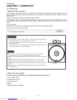
Page 54: ...ystem check 4 Others 5 USB system check_USB play Parts code 1 CD optical pickup Lens cleaner disc UDSKA0004AFZZ HOW TO USE CAUTION Cleaning fluid Cleaner disc Using the brush in the cleaner cap apply 1 or 2 drops of the cleaning fluid to the brush on the CD cleaner disc which has the mark next to it Place the CD cleaner disc onto the CD disc tray with the brush side down then press the play button...

Page 55: ... DISC is displayed 1 Focus system check Press the Tray1 CD Eject Button without inserting a disc and try starting the playback operation Figure 1 126 127 1 2 U10 U10 FOO TRO 1 Does the pickup move No Sled motor Yes 2 Does the focus lens move up and down Waveform drawing Figure 1 No Check the focus peripheral circuit Yes 3 Is the laser lit No Check the laser diode driver Q5 peripheral circuit Yes 4...

Page 56: ...ut play is not possible Yes A normal jump operation cannot be completed or the beginning of the track cannot be found Check the around pin 127 on U10 U10 U10 126 14 4 1 FOO TEI Figure 3 3 Spin system check Press the OPEN CLOSE switch without inserting a disc and then try starting the play operation 1 The turntable rotates a little Waveform drawing Figure 4 Yes The spin driver circuit is OK No 2 Th...

Page 57: ...uits Yes If OK Check the unit U10 U10 6 7 LINEOUTL LINEOUTR 33 36 Figure 5 5 USB system check_USB play Press USB function insert the USB memory device into the USB 1 Does the device information can display No Check around pin 52 and 53 on U10 Figure 6 2 The waveform and the time is displayed normal but no sound is produced No Check the audio out peripheral circuits Figure 6 U10 U10 DP DM 52 53 10 ...

Page 58: ...UT RCLK SCLK SDIO DFS GPO3 DCLK GPO2 INT GPO1 NC NC 1 6 2 3 4 5 16 17 18 19 20 11 10 9 8 7 15 14 13 12 DOUT LOUT ROUT GND VDD FMI RFGND GND PAD AMI RST RST SEN AMI FMI VDD 2 7 5 5 V GND RFGND AM ANT FM ANT DFS GPO DCLK ROUT LOUT VIO 1 5 3 6 V LNA LNA LDO AGC AGC AFC ADC ADC DSP LOW IF RDS Si4731 DIGITAL AUDIO Si4731 CONTROL INTERFACE DAC DAC SEN SCLK RCLK VIO SDIO ...

Page 59: ...erial data input output 9 RCLK External reference oscillator input 10 V10 I O supply voltage 11 VDD Supply voltage May be connected directly to battery 12 GND PAD GND Ground Connect to ground plane on PCB 13 ROUT Right audio line output in analog output mode 14 LOUT Left audio line output in analog output mode 15 DOUT Digital output data in digital output mode 16 DFS Digital frame synchronization ...

Page 60: ...oost MIC in MUX DAC CD servo controller decoder FM in MUX L R Line Out Line in CD ECC System buffer Motor driver Pickup Head Micro Controller Cache Serial Flash USB host Controller USB transceiver USB device GPIO SD MMC card MS MS pro card Interface control logic Crystal 16 9344MHz Linear regulator 3 3V 1 8V Figure 8 2 BLOCK DIAGRAM OF IC ...

Page 61: ...DATA0 GPIOG4 USI_CLK GPIOG3 USI_DI GPIOG2 USI_DO VDD_PAD GND_PAD GPIOF3 SD_MS_DET GPIOF2 SD_MS_PWR GPIOF1 SD_MS_CLK GPIOF0 SDCMD MSBS GPIOE7 SDD3 GPIOE6 SDD2 GPIOE5 SDD1 GPIOE4 SDD0 GPIOE3 SD_MS_WP GPIOE2 DOCD_CLK GPIOE1 DOCD_DATI GPIOE0 DOCD_DATO GPIOD7 SPDIF GPIOD6 12S_WCLK GPIOD5 12S_DI GPIOD4 12S_DO GPIOD3 12S_REFCLK GPIOD2 12S SCLK GPIOD1 12CM_DAT 39 40 41 42 43 44 45 46 47 48 49 50 51 52 53 ...

Page 62: ...Multiplexer output 2 for Analog Signal Monitoring 15 MPXOUT3 O A Multiplexer output 3 for Analog Signal Monitoring 16 COSP O A External Capacitor Connection of Offset Cancellation Loop for VGA in EQRF Block Positive 17 COSN O A External Capacitor Connection of Offset Cancellation Loop for VGA in EQRF Block Negative 18 AVDD33_3 P PRML ADC Power 19 VTB B O PRML ADC Voltage Control connect to Capacit...

Page 63: ...ference 49 VREF O A Internal resistor string provide Vref 50 SFGP I A DISC stop pos input GPIO 51 SFGN I A DISC stop neg input GPIO 52 DM USB D 53 DP USB D 54 VDD_CORE P Digital Core power 55 GND_CORE G Digital Core ground 56 GND_PAD G Digital PAD Ground 57 VDD_PAD P Digital PAD power 58 GPIOB6 SFDO B D GPIOB6 Seriel flash data input 59 GPIOB7 SFDI B D GPIOB7 Seriel flash data output 60 GPIOC0 SFC...

Page 64: ...B D GPIOG3 88 GPIOG4 B D GPIOG4 89 GPIOG5 LCDDB0 B D GPIOG5 LCD data0 90 GPIOG6 LCDDB1 B D GPIOG6 LCD data1 91 GPIOG7 LCDDB2 B D GPIOG7 LCD data2 92 GPIOH0 LCDDB3 B D GPIOH0 LCD data3 93 GPIOH1 LCDDB4 B D GPIOH1 LCD data4 94 GPIOH2 LCDDB5 B D GPIOH2 LCD data5 95 GPIOH3 LCDDB6 B D GPIOH3 LCD data6 96 GPIOH4 LCDDB7 B D GPIOH4 LCD data7 97 GPIOH5 LCDRS B D GPIOH5 LCD status command 98 GPIOH6 LCDCSJ B...

Page 65: ... ground 115 VDD_CORE P Digital Core power 116 AVDD_D33 P 3 3V for digital circuit in analog 117 BTN_ADIN1 I A Bottom check input connect to servo ADC 118 BTN_ADIN2 I A Bottom check input connect to servo ADC 119 BTN_ADIN3 I A Bottom check input connect to servo ADC 120 VREF16 O A SERVO DAC common mode voltage 121 FMO O A Focus servo output 3 level PWM output 122 AVDD33_1 P Servo Analog Power 123 D...

Page 66: ... 1g 1p 1e 1n 1r 1c 2a 2b 1b 2j 2k 2h 2f 2m 2d 2g 2p 2e 2n 2r 2c 1a 1j 1k 1h 1f 1m 1d 1g 1p 1e 1n 1r 1c 2a 2b 1b 2j 2k 2h 2f 2m 2d 2g 2p 2e 2n 2r 2c 1a 1j 1k 1h 1f 1m 1d 1g 1p 1e 1n 1r 1c 2a 2b 1b 2j 2k 2h 2f 2m 2d 2g 2p 2e 2n 2r 2c 1a 1j 1k 1h 1f 1m 1d 1g 1p 1e 1n 1r 1c 2a 2b 1b 2j 2k 2h 2f 2m 2d 2g 2p 2e 2n 2r 2c 1a 1j 1k 1h 1f 1m 1d 1g 1p 1e 1n 1r 1c 2a 2b 1b 2j 2k 2h 2f 2m 2d 2g 2p 2e 2n 2r 2c ...

Page 67: ...ir Component parts no supply S X Category Repair and Replacement PWB can repair and replace KG Category Revolve repair by Business Center Return to Business Center and repair by manufacturer Component parts no supply Explanation of capacitors resistors parts codes Capacitors VCC Ceramic type VCK Ceramic type VCT Semiconductor type VC MF Cylindrical type without lead wire VC MN Cylindrical type wit...

Page 68: ...GR 1 AB Silicon NPN KTC3875 GR Q503 VSKTC3205Y 1 AD Silicon NPN KTC3205 Y Q504 VSKTC3875GR 1 AB Silicon NPN KTC3875 GR Q506 VSKTC3203Y 1 AC Silicon NPN KTC3203 Y Q507 VSKRC104S 1 AC Digital NPN KRC104 S Q601 VSKRA102S 1 AB Digital PNP KRA102 S Q602 VSKTC3875GR 1 AB Silicon NPN KTC3875 GR Q603 VSKTC3875GR 1 AB Silicon NPN KTC3875 GR Q604 VSKTC3875GR 1 AB Silicon NPN KTC3875 GR Q605 VSKTC3875GR 1 AB...

Page 69: ...con 1N4004S D815 VHD1N4004S 1 AB Silicon 1N4004S D842 VHD1N4004S 1 AB Silicon 1N4004S D843 VHD1N4004S 1 AB Silicon 1N4004S D844 VHD1N4004S 1 AB Silicon 1N4004S D845 VHD1N4004S 1 AB Silicon 1N4004S D846 VHD1N4004S 1 AB Silicon 1N4004S D851 VHDMA111G 1 AB Silicon MA111 D852 VHDHSS4148 1 AA Silicon HSS4148 D853 VHD1N4004S 1 AB Silicon 1N4004S D854 VHDHSS4148 1 AA Silicon HSS4148 D855 VHDMA111G 1 AB S...

Page 70: ...mpedence 300 FB63 92L10606030008 AA Impedence 300 FB64 92L10606030008 AA Impedence 300 FB65 92L10606030008 AA Impedence 300 FB66 92L10606030008 AA Impedence 300 FB67 92L10606030008 AA Impedence 300 FB68 92L10606030008 AA Impedence 300 FB69 92L10606030008 AA Impedence 300 FB70 92L10606030008 AA Impedence 300 FB71 92L10606030008 AA Impedence 300 FB72 92L10606030008 AA Impedence 300 FB73 92L106060300...

Page 71: ...9 92L104184K0601 0 18 µF 50V C20 92L104105M0606 1 µF 50V Electrolytic C21 92L104105M0601 AA 1 µF 50V C22 92L104472K0601 4700 pF 50V C23 92L104105M0606 1 µF 50V Electrolytic C24 92L104104Z0601 AA 0 1 µF 50V C25 92L104105M0606 1 µF 50V Electrolytic C26 92L104105M0601 AA 1 µF 50V C27 92L104105M0606 1 µF 50V Electrolytic C28 92L104472K0601 4700 pF 50V C29 92L104105M0606 1 µF 50V Electrolytic C30 92L10...

Page 72: ...02K0601 1000 pF 50V Use in Servo PWB B C110 VCKYCY1HB102K AA 0 001 µF 50V Use in iPOD PWB C C111 VCCCCY1HH101J AA 100 pF CH 50V C112 92L104104Z0601 AA 0 1 µF 50V Use in Servo PWB B C112 VCKYCY1HB102K AA 0 001 µF 50V Use in iPOD PWB C C113 92L104475M0601 4 7 µF 50V Electrolytic Use in Servo PWB B C113 VCKYCY1EF104Z AA 0 1 µF 25V Use in iPOD PWB C C114 92L104107M0406 100 µF 25V Electrolytic Use in S...

Page 73: ...1EW476M AB 47 µF 25V Electrolytic C517 VCEAZA1HW106M AB 10 µF 50V Electrolytic C518 VCEAZA1CW477M AC 470 µF 16V Electrolytic C519 VCEAZA1HW475M AB 4 7 µF 50V Electrolytic C520 VCCCCY1HH101J AA 100 pF CH 50V C523 VCEAZA1HW105M AB 1 µF 50V Electrolytic C528 VCEAZA1EW476M AB 47 µF 25V Electrolytic C530 VCKYTV1HB334K AC 0 33 µF 50V C531 VCKYCY1HB102K AA 1000 pF 50V C532 VCKYCY1CB823K AB 0 082 µF 16V C...

Page 74: ...µF 50V Electrolytic C822 VCEAZA1HW477M AD 470 µF 50V Electrolytic C841 VCEAZA1CW108M AE 1000 µF 16V Electrolytic C842 VCEAZA1VW477M AD 470 µF 35V Electrolytic C843 VCFYFA1HA473J AB 0 047 µF 50V Thin Film C844 RC KZ002LAWZZ AC 0 047 µF 250V Ceramic C851 VCEAZA1EW227M AC 220 µF 25V Electrolytic C852 VCEAZA1HW106M AB 10 µF 50V Electrolytic C853 VCEAZW1EW688M AL 6800µF 25V Electrolytic C854 VCEAZA1HW2...

Page 75: ...5 VCKYCY1HB473K AB 0 047 µF 50V C986 VCEAZA1VW477M AD 470 µF 35V Electrolytic C987 VCEAZA1VW477M AD 470 µF 35V Electrolytic C988 VCKYCY1EF104Z AA 0 1 µF 25V C989 VCKYCY1EF104Z AA 0 1 µF 25V C992 VCKYPA1HB101K AA 100 pF 50V C993 VCKYCY1HB104K AD 0 1 µF 50V E1 92L104107M0201 100 µF 10V Electrolytic E2 92L104106M0407 10 µF 25V Electrolytic E3 92L104107M0406 100 µF 25V Electrolytic E4 92L104476M0401 A...

Page 76: ...s 1 10W R10 92L1011004J021 AA 1 Mohms 1 10W R11 92L1014702J021 AA 47 kohms 1 10W R12 92L1013301J021 AA 3 3 kohms 1 10W R13 92L1011201J021 1 2 kohms 1 10W R14 92L1011002J021 AA 10 kohms 1 10W R15 92L1018201J021 8 2 kohms 1 10W R17 92L1011003J021 AA 100 kohms 1 10W R18 92L1011002J021 AA 10 kohms 1 10W R19 92L1011000J021 AA 100 ohms 1 10W R20 92L1015601J021 AA 5 6 kohms 1 10W R22 92L1012701J021 2 7 k...

Page 77: ...R121 VRS CY1JB104J AA 100 kohms 1 16W Use in iPOD PWB C R122 92L1011002J021 AA 10 kohms 1 10W Use in Servo PWB B R122 VRS CY1JB104D AA 100 kohms 1 16W Use in iPOD PWB C R123 92L1010000J021 AA 0 ohms 1 10W Use in Servo PWB B R123 VRS CY1JB104D AA 100 kohms 1 16W Use in iPOD PWB C R124 92L1010000J021 AA 0 ohms 1 10W R125 92L1011002J021 AA 10 kohms 1 10W R126 92L1011002J021 AA 10 kohms 1 10W R127 92L...

Page 78: ...S CY1JB332J AA 3 3 kohms 1 16W R415 VRS CY1JB330J AA 33 ohms 1 16W R416 VRS CY1JB330J AA 33 ohms 1 16W R417 VRS CY1JB104J AA 100 kohms 1 16W R418 VRS CY1JB104J AA 100 kohms 1 16W R419 VRS CY1JB392J AA 3 9 kohms 1 16W R420 VRS CY1JB392J AA 3 9 kohms 1 16W R421 VRS CY1JB333J AA 33 kohms 1 16W R422 VRS CY1JB333J AA 33 kohms 1 16W R423 VRS CY1JB102J AA 1 kohms 1 16W R424 VRS CY1JB102J AA 1 kohms 1 16W...

Page 79: ...VRS CY1JB102J AA 1 kohms 1 16W R706 VRS CY1JB102J AA 1 kohms 1 16W R707 VRS CY1JB102J AA 1 kohms 1 16W R708 VRS CY1JB102J AA 1 kohms 1 16W R712 VRS CY1JB223J AA 22 kohms 1 16W R752 VRD ST2EE181J AA 180 ohms 1 4W R765 VRD ST2EE1R5J AA 1 5 ohms 1 4W R766 VRD ST2EE1R5J AA 1 5 ohms 1 4W R767 VRS CY1JB272J AA 2 7 kohms 1 16W R768 VRS CY1JB272J AA 2 7 kohms 1 16W R769 VRS CY1JB101J AA 100 ohms 1 16W R77...

Page 80: ...606 Bi902 QCNWNB338AWPZ Connector Ass y 13 12 Pin with CNS801 CNP101 QCNCWA046AW30 AQ Connector 30 Pin CNP102 QCNCWXC16AFZZ AF Connector 16 Pin CNP102A QCNCWYH16AWZZ AD Connector 16 Pin CNP300 QCNCM704BAFZZ AA Connector 2 Pin CNP301 QCNCM704BAFZZ AA Connector 2 Pin CNP302 QCNCM704BAFZZ AA Connector 2 Pin CNP401 92L1200TJH39A1 Connector 9 Pin CNP402 QCNCM704CAFZZ AB Connector 3 Pin CNP402A 92L1200T...

Page 81: ...g Terminal LUG5 QCNWN1860AWZZ AC Lug Wire LUG7 QCNWNA673AWPZ AD Lug Wire LUG802 QLUGP0002AWZZ AB Lug LUG803 QCNWNA980AWPZ AD Lug Wire LUG851 QCNWNB368AWPZ Lug Wire RL841 RRLYDA002AWZZ AF Relay RX701 VHLK2013TH2E1 AG Remote Sensor SO901 QTANAA021AWZZ AD Terminal Speaker SW701 92LSWICHT1663T AC Switch Key Type POWER ON STAND BY SW702 92LSWICHT1663T AC Switch Key Type FUNCTION SW703 92LSWICHT1663T AC...

Page 82: ...x 2 PWB D Q905 608 603 x 3 210 602 x 2 610 x 3 PWB A6 215 221 x 2 214 229 602 601 FROM POWER PWB PWB A5 606 x 2 201 232 231 230 209 204 205 213 221 x 2 613 x 2 201 4 201 5 201 1 201 2 201 8 201 6 201 6 201 3 201 11 201 9 201 12 201 10 201 7 PWB B1 608 x 4 211 203 301 302 x 4 303 x 4 304 x 4 216 220 227 614 x 2 608 609 x 2 608 x 4 PWB C 612 x 2 IC901 IC301 212 x 2 226 228 614 x 4 224 228 606 606 PW...

Page 83: ...nger Unit 217 LHLDZA047AWZZ AC Holder LED 218 LHLDZA199AWZZ AD Holder FL Display 219 LHLDZA243AWSA AD Holder PWB 220 LX LZ0002AW00 AC Rivet 221 PCUSGA133AWZZ AB Cushion Leg 222 PFLT A138AWZZ AB Felt 223 PRDARA197AWFW AL Heat Sink IC 224 PRDARA198AWFW AK Heat Sink Amp 225 PRDARA202AWFW AH Heat Sink IC 226 PRDARA203AWFW AF Heat Sink IC 227 PSHEPA125AWZZ AD Sheet 228 PSHEZA149AWZZ AG Sheet Heat Trans...

Page 84: ...KER LED PWB E FRONT SPEAKER LED PWB E 2 1 2 1 2 1 SDPB40F2A 2 1 2 1 2 1 LED703 R CH 7A 70 CNP CH L CNP708A R CH R752B R CH BK GY BK GY LED702 L CH R752A L CH R752A for L CH LED702 L CH CNP707A for L CH R752B for R CH LED703 R CH CNP708A for R CH COLOR TABLE GY GRAY BLACK BK Lead free solder indication Lead free solder is used in the FRONT SPEAKER LED PWB Refer to Precautions for handling lead free...

Page 85: ...ront Panel Ass y 902 GBOXSA224AW01 Wooden Box Ass y 903 PCUSGA020AWZZ AB Cushion Leg 904 PFLT A012AWZZ AC Felt 905 TSPC B324AWZZ Label Specification 906 XEBY730P10000 AA Screw M3 x 10mm 907 XEPY740P16000 AB Screw M4 x 16mm 908 XESY730P10000 AA Screw M3 x 10mm SP1 2 RSP ZA323AWZZ Woofer SP3 4 RSP ZA321AWZZ AT Tweeter ...

Page 86: ...K SUBWOOFER LED PWB F COLOR TABLE GY GRAY BLACK BK R550 R550 LED504 LED504 CNS502A CNS502B TO MAIN PWB A CNP302 TO MAIN PWB A CNP302 SUBWOOFER LED PWB F BLACK SP1 SUBWOOFER SP1 SUBWOOFER 901 909 905 x 4 904 902 908 x 4 903 SP1 907 x 2 FROM BOX ASSY 906 x 2 907 x 2 PWB F ...

Page 87: ...Case 8 SPAKP0032AWZZ AF Polyethylene Bag Unit 9 SSAKAA011AWZZ AB Polyethylene Bag Accessories 10 SSAKHA170AWZZ AE Polyethylene Bag Subwoofer 11 SSAKHA077AWZZ AD Polyethylene Bag Front Speaker 12 TCAUZA160AWZZ AC Special Notes 13 TiNSZA536AWZZ AD Operation Manual For Central South America 13 TiNSZA625AWZZ Operation Manual For U S A 14 TLABZB040AWZZ Label Pop For U S A 14 TLABZB050AWZZ AD Label Pop ...

Page 88: ... No part of this publication may be reproduced stored in a retrieval system or transmitted in any form or by any means electronic mechanical photocopying recording or otherwise without prior written permission of the publisher S O Electronics Malaysia Sdn Bhd Sungai Petani Kedah Malaysia SHARP CORPORATION ...

Reviews: