DV-L70S
DV-L70BL
DV-L70W
34
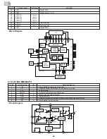
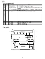
9-12. IC702 BA5933FP-1
Pin No.
Terminal name
Operation function
Pin No. Terminal name
Operation function
1
STBY
Stand-by mode selector switch
13
OP_OUT
Operation amplifier output
2
OUT+
CH1 positive output terminal
14
OP_IN(-)
Operation amplifier negative input
3
OUT-
CH1 negative output terminal
15
OP_IN(+)
Operation amplifier positive input
4
GND
GND
16
IN2'
CH2 gain adjustment input terminal
5
VCC
VCC
17
IN2
CH2 gain fixed input terminal
6
MUTE
Mute terminal
18
IN3'
CH3 gain adjustment input terminal
7
GND
Substrate GND
19
IN3
CH3 gain fixed input terminal
8
REG_OUT
Constant voltage output
20
VCC
VCC
(collector of external Tr)
21
GND
GND
9
REG_B
Connected to the base of external Tr
22
OUT3-
CH3 negative output terminal
10
BIAS
Bias input terminal
23
OUT3+
CH3 positive output terminal
11
IN1'
CH1 gain adjustment input terminal
24
OUT2-
CH2 negative output terminal
12
IN1
CH1 gain fixed input terminal
25
OUT2+
CH2 positive output terminal
* The negative/positive pole of the output terminal is the polarity against the input.
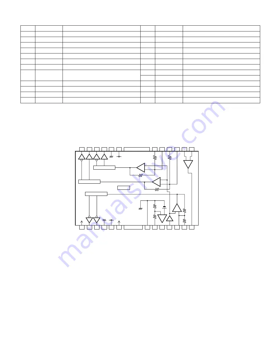
• Block Diagram
LEVEL SHIFT
LEVEL SHIFT
LEVEL SHIFT
T.S.D.
x2
x2
x2
x2
x2
x2
+ -
+ -
+ -
+ -
+ -
25
24
23
22
21
20
19
18
17
16
15
14
1
2
3
4
5
6
8
9
7
10
11
12
13
STBY
MUTE
8.3K
Ω
8.3K
Ω
8.3K
Ω
8.3K
Ω
8.3K
Ω
10K
Ω
10K
Ω
8.3K
Ω
REGULATOR
OP-AMP
T.S.D ; Thermal shutdown
Unit of resistance is [
Ω
].
Summary of Contents for DV-L70BL
Page 2: ...DV L70S DV L70BL DV L70W 2 1 IMPORTANT SAFEGUARDS AND PRECAUTIONS ...
Page 6: ...DV L70S DV L70BL DV L70W 6 For details on the use of each control 4 PART NAMES ...
Page 53: ...53 DV L70S DV L70BL DV L70W 11 WIRING DIAGRAM ...
Page 82: ...Ref No Part No Description Code Ref No Part No Description Code 95 DV L70S DV L70BL DV L70W ...


