background image

Ref. No.

Part No.

Description

Code

Ref. No.

Part No.

Description

Code

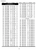
131

DV-NC55U/C/M

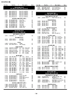
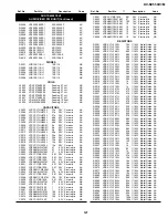
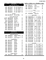
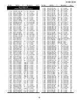
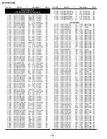
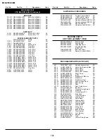
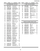
C1507

VCKYCY1CF104Z

0.1

16V Ceramic

AA

C1508

VCEA9M1HW475M

4.7

50V Electrolytic

AB

C1509

VCKYCY1HF103Z

0.01

50V Ceramic

AA

C1512

VCKYCY1HF103Z

0.01

50V Ceramic

AA

C1513

VCKYCY1HF103Z

0.01

50V Ceramic

AA

C1514

VCKYCY1HF103Z

0.01

50V Ceramic

AA

C1515

VCKYCY1HB331K

330p 50V Ceramic

AA

C1517

VCEA9M1HW335M

3.3

50V Electrolytic

AB

C1518

VCKYCY1CB333K

0.033 16V Ceramic

AA

C1521

VCCCCY1HH5R0C

5p

50V Ceramic

AA

C1523

VCKYCY1HF103Z

0.01

50V Ceramic

AA

C1524

VCKYCY1HF103Z

0.01

50V Ceramic

AA

C1601

VCEA9M0JW107M

100

6.3V Electrolytic

AB

C1602

VCKYCY1EB103K

0.01

25V Ceramic

AA

C1603

VCEA9M1CW106M

10

16V Electrolytic

AB

C1604

VCKYCY1HB821K

820p 50V Ceramic

AA

C1605

VCEA9M1HW475M

4.7

50V Electrolytic

AB

C1606

VCEA9M1HW475M

4.7

50V Electrolytic

AB

C1607

VCEA9M1HW475M

4.7

50V Electrolytic

AB

C1608

VCEA9M0JW226M

22

6.3V Electrolytic

AB

C1609

VCEA9M1HW475M

4.7

50V Electrolytic

AB

C1611

VCKYCY1CF104Z

0.1

16V Ceramic

AA

C1614

VCKYCY1HB222K

2200p 50V Ceramic

AA

C1617

VCEA9M1CW476M

47

16V Electrolytic

AB

C1618

VCKYCY1EB103K

0.01

25V Ceramic

AA

C1619

VCKYCY1EB103K

0.01

25V Ceramic

AA

C1620

VCEA9M1CW106M

10

16V Electrolytic

AB

C1621

VCQPYA2AA562J

5600p 100V Film Condenser AC

C1622

VCKYCY1HB222K

2200p 50V Ceramic

AA

C1623

VCQYTA1HM183J

0.018 50V Mylar

AB

C1624

VCQYTA1HM562J

5600p 50V Mylar

AA

C1625

VCQYTA1HM183J

0.018 50V Mylar

AB

C1630

VCKYCY0JF105Z

1

6.3V Ceramic

AB

C1651

VCEA9M1HW475M

4.7

50V Electrolytic

AB

C1652

VCEA9M0JW336M

33

6.3V Electrolytic

AB

C1653

VCEA9M1CW106M

10

16V Electrolytic

AB

C1654

VCEA9M1CW106M

10

16V Electrolytic

AB

C1655

VCEA9M1CW106M

10

16V Electrolytic

AB

C1657

VCKYCY1EB153K

0.015 25V Ceramic

AA

C1661

VCEA9M1HW475M

4.7

50V Electrolytic

AB

C1662

VCEA9M0JW336M

33

6.3V Electrolytic

AB

C1663

VCEA9M1CW106M

10

16V Electrolytic

AB

C1664

VCEA9M1CW106M

10

16V Electrolytic

AB

C1665

VCEA9M1CW106M

10

16V Electrolytic

AB

C1667

VCKYCY1EB153K

0.015 25V Ceramic

AA

C1670

VCEA9M0JW107M

100

6.3V Electrolytic

AB

C1671

VCEA9M1CW107M

100

16V Electrolytic

AB

C1672

VCKYCY1CF224Z

0.22

16V Ceramic

AA

C1673

VCEA9M0JW226M

22

6.3V Electrolytic

AB

C1674

VCKYCY1CF224Z

0.22

16V Ceramic

AA

C1675

VCKYCY1CF104Z

0.1

16V Ceramic

AA

C1677

VCEA9M1CW106M

10

16V Electrolytic

AB

C1678

VCKYCY1HF103Z

0.01

50V Ceramic

AA

C1679

VCKYCY1CF224Z

0.22

16V Ceramic

AA

C1680

VCKYCY0JF105Z

1

6.3V Ceramic

AB

C1681

VCKYCY1HF103Z

0.01

50V Ceramic

AA

C1682

VCKYCY0JF105Z

1

6.3V Ceramic

AB

C1684

VCCCCY1HH560J

56p

50V Ceramic

AA

C1685

VCCCCY1HH560J

56p

50V Ceramic

AA

C1686

VCKYCY1CF104Z

0.1

16V Ceramic

AA

C1687

VCEA9M1CW107M

100

16V Electrolytic

AB

C1688

VCEA9M1CW476M

47

16V Electrolytic

AB

C1689

VCEA9M1CW106M

10

16V Electrolytic

AB

C1690

VCEA9M1CW106M

10

16V Electrolytic

AB

C1691

VCEA9M1CW106M

10

16V Electrolytic

AB

C1692

VCEA9M1CW106M

10

16V Electrolytic

AB

C1693

VCEA9M1CW106M

10

16V Electrolytic

AB

C1694

VCEA9M1CW106M

10

16V Electrolytic

AB

C1701

VCKYCY1HF103Z

0.01

50V Ceramic

AA

C1702

VCKYCY1HF103Z

0.01

50V Ceramic

AA

C1703

VCEA9M1HW105M

1

50V Electrolytic

AB

C1704

VCKYCY0JF105Z

1

6.3V Ceramic

AB

C1705

VCKYCY1EB103K

0.01

25V Ceramic

AA

C1706

VCKYCY1EB103K

0.01

25V Ceramic

AA

C1707

VCCCCY1HH150J

15p

50V Ceramic

AA

C1160

VCEA9M1HW225M

2.2

50V Electrolytic

AB

C1161

VCKYCY1CB104K

0.1

16V Ceramic

AB

C1162

VCKYCY1CB104K

0.1

16V Ceramic

AB

C1163

VCEA9M1CW106M

10

16V Electrolytic

AB

C1164

VCKYCY1CB104K

0.1

16V Ceramic

AB

C1165

VCKYCY1CB104K

0.1

16V Ceramic

AB

C1166

VCKYCY1EB223K

0.022 25V Ceramic

AA

C1167

VCKYCY1CB104K

0.1

16V Ceramic

AB

C1168

VCEA9M1CW106M

10

16V Electrolytic

AB

C1169

VCEA9M1HW105M

1

50V Electrolytic

AB

C1201

VCEA9M0JW107M

100

6.3V Electrolytic

AB

C1202

VCKYCY0JF105Z

1

6.3V Ceramic

AB

C1203

VCCCCY1HH151J

150p

50V Ceramic

AA

C1204

VCKYCY1CF104Z

0.1

16V Ceramic

AA

C1205

VCCCCY1HH470J

47p

50V Ceramic

AA

C1206

VCKYCY1CF104Z

0.1

16V Ceramic

AA

C1207

VCKYCY1CF104Z

0.1

16V Ceramic

AA

C1208

VCEA9M1CW106M

10

16V Electrolytic

AB

C1209

VCKYCY1CF104Z

0.1

16V Ceramic

AA

C1210

VCKYCY1CB104K

0.1

16V Ceramic

AB

C1211

VCEA9M1HW335M

3.3

50V Electrolytic

AB

C1212

VCEA9M1CW106M

10

16V Electrolytic

AB

C1213

VCEA9M1HW225M

2.2

50V Electrolytic

AB

C1214

VCKYCY0JF105Z

1

6.3V Ceramic

AB

C1215

VCKYCY0JF105Z

1

6.3V Ceramic

AB

C1216

VCKYCY0JF105Z

1

6.3V Ceramic

AB

C1217

VCEA9M0JW107M

100

6.3V Electrolytic

AB

C1218

VCKYCY0JF105Z

1

6.3V Ceramic

AB

C1219

VCKYCY1CF104Z

0.1

16V Ceramic

AA

C1220

VCKYCY1CF104Z

0.1

16V Ceramic

AA

C1221

VCEA9M1CW106M

10

16V Electrolytic

AB

C1223

VCKYCY1CF104Z

0.1

16V Ceramic

AA

C1226

VCEA9M0JW107M

100

6.3V Electrolytic

AB

C1227

VCKYCY0JF105Z

1

6.3V Ceramic

AB

C1228

VCEA9M0JW107M

100

6.3V Electrolytic

AB

C1251

VCEA9A1CW476M

47

16V Electrolytic

AB

C1256

VCKYCY1CF104Z

0.1

16V Ceramic

AA

C1257

VCKYCY1CF104Z

0.1

16V Ceramic

AA

C1258

VCEA9M0JW476M

47

6.3V Electrolytic

AB

C1259

VCKYCY0JF105Z

1

6.3V Ceramic

AB

C1260

VCKYCY1CF104Z

0.1

16V Ceramic

AA

C1261

VCKYCY1HF103Z

0.01

50V Ceramic

AA

C1262

VCEA9M0JW476M

47

6.3V Electrolytic

AB

C1301

VCEA9M0JW107M

100

6.3V Electrolytic

AB

C1302

VCKYCY0JF105Z

1

6.3V Ceramic

AB

C1303

VCKYCY1HB102K

1000p 50V Ceramic

AA

C1304

VCKYCY1HB102K

1000p 50V Ceramic

AA

C1305

VCKYCY1HB102K

1000p 50V Ceramic

AA

C1306

VCKYCY1HB102K

1000p 50V Ceramic

AA

C1307

VCKYCY1HB102K

1000p 50V Ceramic

AA

C1308

VCKYCY1HB102K

1000p 50V Ceramic

AA

C1309

VCKYCY1HB102K

1000p 50V Ceramic

AA

C1310

VCKYCY1HB102K

1000p 50V Ceramic

AA

C1311

VCKYCY1HF103Z

0.01

50V Ceramic

AA

C1312

VCKYCY1HF103Z

0.01

50V Ceramic

AA

C1319

VCCCCY1HH100D

10p

50V Ceramic

AA

C1320

VCCCCY1HH100D

10p

50V Ceramic

AA

C1327

VCKYCY1HB102K

1000p 50V Ceramic

AA

C1329

VCKYCY1HF103Z

0.01

50V Ceramic

AA

C1351

VCEA9M0JW107M

100

6.3V Electrolytic

AB

C1352

VCKYCY0JF105Z

1

6.3V Ceramic

AB

C1353

VCKYCY1HF103Z

0.01

50V Ceramic

AA

C1354

VCKYCY1HF103Z

0.01

50V Ceramic

AA

C1356

VCCCCY1HH101J

100p

50V Ceramic

AA

C1357

VCKYCY1CB104K

0.1

16V Ceramic

AB

C1358

VCKYCY1CB104K

0.1

16V Ceramic

AB

C1501

VCEA9M0JW107M

100

6.3V Electrolytic

AB

C1502

VCKYCY0JF105Z

1

6.3V Ceramic

AB

C1503

VCKYCY1HB472K

4700p 50V Ceramic

AA

C1504

VCEA9M1HW225M

2.2

50V Electrolytic

AB

C1505

VCKYCY1EB223K

0.022 25V Ceramic

AA

C1506

VCEA9M1HW474M

0.47

50V Electrolytic

AB

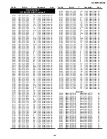
DUNTK6068TEV2

VTR MAIN PWB UNIT(Continued)

Summary of Contents for DV-NC55C

Page 1: ... REPLACEMENT PARTS LIST 123 16 PACKING OF THE SET 142 CONTENTS In the interests of user safety Required by safety regula tions in some countries the set should be restored to its original condition and only parts identical to those specified be used MODELS DV NC55U DV NC55C DV NC55M SERVICE MANUAL VCR DVD COMBINATION MODEL MODELS DV NC55U C M VCR DVD COMBINATION MODEL This document has been publis...

Page 2: ...llic control knobs insulation materials cabinet backs adjustment and compartment covers or shields isola tion resistor capacitor networks mechanical insula tors etc 3 To be sure that no shock hazard exists check for current in the following manner Plug the AC line cord directly into a 120 volt AC outlet Do not use an isolation transformer for this test Using two clip leads connect a 1 5k ohm 10 wa...

Page 3: ...les couvercles de compartiment et ajustement ou les boucliers les réseaux de résistance condensateur d isolement Ies isolateurs mécaniques etc 3 Pour être sûr qu il n y a aucun risque de choc électrique vérifier le courant de fuite de la maniére suivante Brancher le cordon d alimentation secteur directement dans une prise de courant de 120 volts Ne pas utiliser de transformateur d isolement pour c...

Page 4: ...SURROUNDTM is a trademark of QSound Labs Inc 2 Manufactured under license from Dolby Laboratories Dolby Pro Logic and the double D symbol are trademarks of Dolby Laboratories 3 DTS and DTS Digital Surround are trademarks of Digital Theater Systems Inc 3 SPECIFICATIONS Signal System NTSC INPUT OUTPUT JACKS DVD VCR shared output jacks VIDEO jack RCA Pin jack AUDIO jack RCA Pin jack DVD output jacks ...

Page 5: ...udio signal frequency characteristics For DVD linear PCM playback 4 Hz to 22 kHz 48 kHz sampling 4 Hz to 44 kHz 96 kHz sampling CD playback 4 Hz to 20 kHz JEITA S N ratio CD 100 dB 1 kHz EIAJ Dynamic range DVD linear PCM 96 dB CD 96 dB JEITA Total harmonic distortion ratio CD 0 006 JEITA Pickup Wave length 650 nm Laser output Max 0 7 mW Operating temperature 5 C to 35 C 41 F to 95 F Storage temper...

Page 6: ...Indicator Operation status Indicator Cassette compartment VCR Front Panel Display DVD Main Unit Front DVD Front Panel Display REW PLAY STANDBY CH TRACKING POWER EJECT STOP PLAY STOP OPEN CLOSE VCR DVD AV 1 L MONO AUDIO R AV 2 IN VDEO Disc tray OPEN CLOSE POWER TITLE indicator Operation status Time indicator TRACK indicator CHAPTER indicator Disc operation buttons PLAY STOP PROGRAM indicator REPEAT...

Page 7: ...e battery cover by lowering the lid in the direction of the arrow Do not subject the remote control unit to shock water or excessive humidity The remote control unit may not function if the Unit sensor is in direct sunlight or any other strong light Incorrect use of batteries may cause them to leak or burst Read the battery warnings and use the batteries properly Do not mix old and new batteries o...

Page 8: ...TAL AUDIO AUDIO R L S VIDEO DVD VCR AV 1 OUT AUDIO R L VIDEO VCR AV 1 IN AUDIO R VIDEO IN FROM ANTENNA UHF VHF CATV OUT TO T V OUTPUT CHANNEL 3 4 L MONO VCR AUDIO input jacks ANTENA IN antena or cable input VCR VIDEO input jack ANTENA OUT 3 4 OUTPUT CHANNEL select DVD VCR shared AUDIO output jacks DVD Coaxial DIGITAL output jack DVD S VIDEO output jack DVD AUDIO output jacks DVD VCR shared VIDEO o...

Page 9: ...easily damaged by electrostatic charges When handling the pickup take care so that the electrostatic charge is not generated 3 The semiconductor laser may be easily damaged by overcurrent Use the power supply unit which does not give any spike current when the power is turned on and off 4 Carefully remove the dust and dirt from the objective lens with the lens blower When handling the objective le...

Page 10: ...t the PWB toward you to remove it 4 Removing the DVD mechanism 1 Remove the six screws 9 2 Remove the DVD REINF angle 0 3 Remove the connector q 4 Remove the two FFCs w 2 1 1 3 7 6 4 5 6 8 Shild Plate 9 9 10 12 12 11 12 22 21 20 15 16 14 17 16 18 19 23 24 5 Peel the FFC w off the DVD mechanism 6 Remove the FFC r 7 Remove the shield lower t 8 Remove the two FFCs y and at two connectors u and at fou...

Page 11: ... Removing the cassette housing control VTR mechanism 1 Remove the two screws k 2 Remove the two screws l 3 Remove the one screw 4 Remove the H A shield case upper 6 Removing the terminal plate VTR main PWB 1 Remove the four screws 2 Remove the one screw 7 Removing the bottom plate 1 Remove the six screws 31 32 33 34 ...

Page 12: ...in 500mm DVD main CN201 power P9001 QCNW 8601AJZZ AE Extension cable FFC 23pin I F CN8203 DVD display CN5001 QCNW 8605AJZZ AE Extension cable FFC 9pin DVD main CN802 AV CN2005 Power PWB P9001 CN2005 Audio Video PWB Tuner CN8202 CN201 CN802 CN801 CN5001 CN8203 Interface PWB DVD main PWB DVD Mechanism VTR Display PWB DVD Display PWB VTR Mechanism VTR Main PWB QCNW 8571GEZZ 9pin QCNW 8570GEZZ 29pin Q...

Page 13: ...sm chassis to the angle state ground it to prevent the electrostatic discharge damage of the pickup 2 Remove S and the DVD shield lower 56 refer to the illustration on page 140 3 Remove P Q Z and R 83 from the DVD main PWB unit 68 and loosen the 4 screws 45 to remove the DVD main PWB unit 68 Pickup relay FFC 74 isn t removed refer to the illustration on page 140 4 Remove screws fixing the base cha...

Page 14: ...ser light even if the flowing current is slightly varied the projection light is detected with the monitor diode to control the laser light to be equally output Since the current varies on the monitor diode according to the intensity of the received light of the laser diode the drive current of the laser diode is reduced if the current of the monitor diode increases On the contrary the drive curre...

Page 15: ...re used for checking and adjusting the reel disk height When fixing any part to the threaded hole using resin with screw use the jig Specified torque 5 kg This cassette torque meter is used for check ing and adjusting the torque of take up for measuring tape back tension These Jigs are used for checking and adjusting the torque of take up and supply reel disks Master Plane Jig and Reel Disk Height...

Page 16: ...tape contact part with the specified cleaning liquid Clean tape contact area with the specified cleaning liquid Clean rubber and rubber contact area with the specified cleaning liquid Replace the roller of the cleaner when it wears down Just change the AHC roller assembly for new one Screen swaying Cassette not loaded or unloaded No tape running tape slack Tape slack AHC Automatic head cleaner Vid...

Page 17: ...pole base ass y 3 Tension arm 4 Idler wheel ass y 5 Pinch drive lever ass y 6 Supply reel disk 7 Supply main brake 8 Take up main brake 9 Pinch drive cam 10 A C head ass y 11 Reverse guide lever ass y 12 Casecon drive gear 13 Take up reel disk 14 Pinch roller lever ass y 17 15 10 11 5 9 14 12 8 16 13 4 6 2 7 3 1 18 ...

Page 18: ...W No Function No Function 15 Upper and lower drum ass y 16 Loading motor 17 Drum drive motor 18 Take up pole base ass y 19 Slow brake lever 20 Master cam 21 Capstan D D motor 22 Reel belt 23 Clutch lever 24 Limiter pulley ass y 26 Shifter 26 24 21 22 19 20 12 23 ...

Page 19: ...echanism from the main PWB Remove the PWB bottom plate 1 screw 1 Remove the FFC cable AA AD AH 2 which connect ing the PWB and the mechanism Take out vertically the mechanism so that it does not damage the adjacent parts 2 Removing the mechanism and cassette housing Remove 2 screws 3 fixing the cassette housing to the mechanism and remove the cassette housing ...

Page 20: ...al set position 1 install the cassette housing in the specified position This method is applied only for the mechanism INSTALLING THE MECHANISM ON PWB Lower vertically the mechanism paying attention to the mechanism edge and install the mechanism with due care so that the parts are not damaged So as to fix the mecha nism to the main PWB install 1 screw 1 For other fix the vicinity of loading motor...

Page 21: ...using control and tool do not contact the guide pin or drum 5 After installing the cassette housing control once per form cassette loading operation 8 7 TORUNATAPEWITHOUTTHECASSETTE HOUSING CONTROL ASSEMBLY 1 Remove the full surface panel 2 Short circuit between TP5102 and TP5103 3 Plug in the power cord 4 Turn off the power switch The pole bases move into U L position 5 Open the lid of a cassette...

Page 22: ...check the video search rewind back tension see 8 13 and check the brake torque see 8 17 Height checking and adjustment Note 1 Set the master plane with due care so that it does not contact the drum 2 When putting the master plane shift the reverse guide a little in the loading direction Care must be taken since excessive shift results in damage Figure 8 6 Note 1 Check that the reel disk is lower t...

Page 23: ...circuiting between TP5102 and TP5103 provided goes left at VTR display PWB plug in the power cord Setting 1 Set a torque gauge to zero on the scale Place it on the take up reel disk 2 Press the FF button 3 To calculate the remaining capacity of the play back mode slowly rotate the supply reel disk and then shift it into the forward mode Checking 1 Turn the torque gauge slowly one rotation every 2 ...

Page 24: ... disk and turn it counterclockwise very slowly one rotation every 1 to 2 seconds and check that the torque is within the set value 14 0 3 9mN m 144 40gf cm Set value EP6 9 2 5mN m 70 25gf cm 500g Cassette torque meter Figure 8 10 Checking 1 Make sure that value is within the setting 6 9 2 5mN m 70 25gf cm 2 The winding up torque fluctuates due to variation of rotation torque of limiter pulley ass ...

Page 25: ...ent with the beginning of a T 120 tape 8 13 CHECKING THE VIDEO SEARCH REWIND BACK TENSION Remove the cassette housing control assembly After short circuiting between TP5102 and TP5103 provided goes left at VTR display PWB plug in the power cord Checking 1 After pressing the play button press the rewind button and set the video search rewind mode 2 Place the torque gauge on the take up reel disk an...

Page 26: ... of tension pole adjuster is within 90 range left right 8 16 CHECKING AND ADJUSTMENT OF RECORD PLAYBACK BACK TENSION Remove the cassette housing control assembly After short circuiting between TP5102 and TP5103 provided goes left at VTR display PWB plug in the power cord Turn off the power switch Setting 1 Open the torque cassette meter and fix with tape 2 Set the cassette tape in loading state 3 ...

Page 27: ...torque at the supply side and the take up side Unless the supply side brake torque or take up side brake torque is within the setting clean the felt surface of reel disk supply take up brake lever check again the brake torque If value cannot be set within the setting yet replace the main brake ass y or main brake spring Figure 8 20 8 17 CHECKING THE BRAKE TORQUE Checking the brake torque at the su...

Page 28: ...ate unplug the power cord Removal 1 Remove the screws 123 Azimuth screw Tilt screw 2 Unsolder the PWB fitted to the A C head Notes 1 When replacing never touch the head If you touched clean with the cleaning liquid 2 When removing the screw 3 take care so that the spring may out New A C head ass y A C head PWB 2 Spring 1 Solder Never touch the head 10 8mm 10 8mm Azimuth screw Height screw Tilt scr...

Page 29: ...ssis to the reverse guide lower flange to 13 38 mm using the reverse guide height adjustment jig in tape loading state Refer to Figure 8 28 a b Figure 8 29 3 Set the tape and check for tape crease near the reverse guide in the playback mode If crease is found turn the reverse guide adjustment nut to remove crease As for crease check refer to Figure 8 30 a b Figure 8 28 2 Rotate counterclockwise th...

Page 30: ...ockwise so that tape crease appears once at the flange and then return the tilt screw so that the crease disappears 2 If there is tape crease Turn counterclockwise the tilt screw so that the tape crease disappears Reference If the tilt screw is turned clockwise crease appears at the lower flange Guide roller Weight of 500g Cassette Tape 2 Adjustment of A C head height and azimuth 1 Perform the ini...

Page 31: ...ustment method 6 Playback the self picture recorded tape and check the flatness of ATR signal waveform and sound Notes When the A C head X value adjustment is performed be sure to perform at first X value rough adjustment refer to 8 21 3 2 PB CHROMA Signal Head switching pulse Figure 8 34 4 A C head X value adjustment 1 Tentatively fix A C head arm screws 1 and 2 by the method described in 8 18 Re...

Page 32: ...er to 8 4 item 1 When removing the mechanism from the main PWB Removal Follow the order of indicated numbers 1 Remove the reel belt 1 2 Remove the slow brake lever 2 3 Remove the three screws 3 Reassembly 1 Taking care so that the capstan shaft does not contact the mechanism chassis set its position on the mecha nism chassis and then install with the three screws 3 2 Install the slow brake lever 2...

Page 33: ...PER AND LOWER DRUM ASSEMBLY Replacement Perform in the numerical order 1 Remove the motor as stated in 8 23 D D motor replace ment 2 Remove the drum earth brush ass y 2 3 Remove the drum base 3 from the upper and lower drum assembly 1 Cares when replacing the drum 1 Be careful so that the drum earth brush is not lost 2 Do not touch directly the drum surface 3 Fit gently the screwdriver to the scre...

Page 34: ...ss y 3Insert Open Lever Insert reverse guide lever ass y Align here 2 Insert pinch drive cam Pinch drive lever ass y Fit the pinch drive cam so that the notch of pinch drive cam aligns with the dent of pinch drive lever assembly Fit the pinch drive cam so that the notch of pinch drive lever assembly aligns with the half round notch of chassis Turn the reverse guide lever assembly counterclockwise ...

Page 35: ...the phase matching at the insert point 1 see the Phase Matching point 2 as shown below 4 Finally fix the inserts 1 and 4 Capstan D D motor Drum Reel pulley Bottom side of mechanism chassis Sifter Phase Matching point 2 Insert point 1 Half round notch Shaft 1 Round mark Loading gear T Insert point 3 Insert point 4 Insert point 5 Release point 3 Phase matching point 1 Shaft 1 Shaft 1 Shaft 4 Insert ...

Page 36: ...emove the loading motor and install the replacement loading motor as shown below Figure 8 47 Figure 8 45 2 When installing the master cam align the casecon drive gear round mark with the half round notch of master cam The loading motor pressing in must be less than 14 7 N 1 500 gf Adjust the distance between motor and pulley to 10 2 mm E ring XRESJ30 06000 Master cam Fully turn clockwise Fully tur...

Page 37: ...ve Gear R 8 29 ASSEMBLY OF CASSETTE HOUSING 1 Drive Gear and R Drive angle ass y Figure 8 48 MSPRT0381AJFJ Apply grease Apply grease Apply grease LANGF9592AJFW Top surface should be free from scratches or soil Drive angle Drive gear R Frame Figure 8 49 ...

Page 38: ...o the test mode initial image plane The playback key of the remote controller is pushed The playback key of the remote controller is pushed There is no copy guard signal As for the symptom when it was dubbed in the video tape recorder Color bar display 00002 FIP The playback key of the remote controller is pushed The playback key of the remote controller is pushed AGC only As for the symptom when ...

Page 39: ...cus on STEP TEST 30000201 00000000 Playback Key input RF gain adjustment Track on STEP TEST 30000202 00000000 Playback Key input Focus gain adjustment STEP TEST 30000203 00000000 Playback Key input Track gain adjustment STEP TEST 30000204 00000000 Laser test mode STEP TEST 30000001 00000000 2 Key input Step execution mode To 2 STEP TEST 30000205 00000000 Focus balance adjustment STEP TEST DD000211...

Page 40: ...in the section ROM RENEWAL MODE 1 A DVD itself and a personal computer are articulated as the right figure Software for the renewal is started more 2 A power source is put with pushing a DVD s own playback key and a halt key at the same time It keeps pushing it for about three seconds 3 When Y is inputted in accordance with the personal computer display and data transfer indication is shown and re...

Page 41: ...ol receiver and the pin 10 of IC8201 Is the L pulse sent out pin 1 terminal of receiver when the infrared remote control is activated Is pulse signal supplied to the pin 10 of IC8201 Check the line between the remote control receiver and the pin 32 of IC504 Replace IC504 Replace IC8201 Is pulse signal supplied to the pin 32 of IC504 No No No No Yes No Yes Yes Yes Yes No operation is possible from ...

Page 42: ...ot light Both picture and sound do not operate normally 1 Note Since the laser diode is very susceptible to static electricity be careful of static electricity or electricity leak from the measuring equipment when confirming the voltage FLOW CHART NO 9 Check the PC 5V line Set the disc on the disc tray Are the video signals outputted to the pins of main unit connector CN802 CN802 1PIN CVBS Y CN802...

Page 43: ...UT Yes Are the system control interface signals inputted to the pins of IC6001 IC6001 26PIN ADAC DA IC6001 27PIN ADAC CK IC6001 28PIN ADAC L IC6001 22PIN RSTO I 1 2 3 Check the DVD H line and Q6010 No Replace IC6010 Yes Is 9V applied to the pin 16 of IC6010 Are the audio interface signals outputted to the pins of IC6010 IC6010 15PIN L OUT IC6010 14PIN R OUT No No Are the pins 9 10 and 11 of IC6010...

Page 44: ...ontrol transmitter if necessary Is inputted L pulse to pin 5 of IC1701 Check line between at remote control receiver thru to pin 5 of IC1701 Replace IC1701 NO NO NO YES YES YES YES No operation is possible from the infrared remote control FLOW CHART NO 5 Does the start sensor pulse at pin 79 of IC1701 change from L to H level when the cassette tape is loaded Check line start sensor and all the way...

Page 45: ...in 4 of IC1701 change from L to H level Check IC1701 Does the base of Q1951 change from about 5 0V to 4 5V Check the pin 4 of IC1701 and all the way up thru to Q1952 Is 5V sent out of the collector of Q1951 Check Q1951 and the STBY 5V line NO NO NO YES YES No power is turned on FLOW CHART NO 9 Is the voltage more than about 2 6V DC given out of pin 46 of IC1701 Check IC1701 Is the supply voltage o...

Page 46: ... CTL signal output at pins 75 and 74 of IC1701 Is the V SYNC signal reference at pin 50 of IC1701 Check peripheral circuit of C1770 1 and R1770 Is there capstan AFC and APC at pins 31 and 33 of IC1701 Capstan servo does not function FLOW CHART NO 14 NO YES YES NO YES NO YES NO YES NO NO NO NO YES YES Is picture signal input into pins 30 28 and 31 of IC1201 Is picture signal output to the pin 52 of...

Page 47: ... between the pins 58 and 35 of IC1201 Check R1505 C1515 Check whether the pins 71 and 73 of IC1201 oscillate 3 58 MHz Check between the pins 60 and 46 of IC1201 Check C1512 Is chroma signal approx 143 mVp p Burst input into the pin 46 of IC1201 Is chroma signal approx 180 mVp p Burst input into the pin 58 of IC1201 Check between the pins 21 and 42 of IC1201 Check C1208 Check between the pins 39 an...

Page 48: ... of IC1201 Check C1212 Is luminance signal approx 0 5 Vp p input to the pin 39 of IC1201 Is voltage 5V applied to the CCD section power terminal pin 36 of IC1201 Is control voltage approx 5V applied normally to the pin 37 from the pin 57 of IC1201 Is CCD clock signal approx 7 16 MHz 0 5 Vp p applied to the pin 44 from the pin 69 of IC1201 Check between the pins 24 and 23 of IC1201 Check C1210 Repl...

Page 49: ...and pin 45 of IC1651 YES Check the line between the pin 59 of IC1651 and the pin 2 of the tuner TU1101 RF output terminal connection Is the audio signal output to the pin 59 of IC1651 Is there SIF signal from pin 22 of Tuner No Hi Fi E E sound heard FLOW CHART NO 18 NO YES NO YES NO YES NO Is terminal voltage REC AGC ADJ pin 37 of IC1651 normal Is record FM signal output to the pins 21 to 24 ch 1 ...

Page 50: ...for short circuiting of circuit and rectifying diode of each rectifying circuit of secondary circuit and check for failure of shunt regulator circuit D9001 D9003 5 D9010 11 D9006 C9009 10 When the output voltage varies When buzz is heard from the vicinity of power circuit NO NO NO NO NO NO NO NO FLOW CHART NO 5 Does the change from STANDBY LED indicate turn off Check the AT 5V line YES Is the supp...

Page 51: ... pin 9 of IC8201 Replace IC8201 Check or replace D9091 8 NO NO NO YES YES YES YES YES NO PC 5V is not output FLOW CHART NO 9 Is 19V voltage supplied at emitter of Q8202 Check the AT 19V line Is voltage of 19V sent out from the collector of Q8202 Check for load circuit short circuiting or leak Check the Q8202 periphery circuit Are the H pulse inputted into the pin 32 of IC8201 Does the P CON switch...

Page 52: ...t Mute 23 VccS Power terminal servo 24 NC Used in the open state 25 RPZ O RF ripple output 2 VrD 26 RPO O RF ripple output 1 VrD 2 27 RPB RF ripple bottom 28 RPP RF ripple peak 29 RFOn O Equivalent RF output 1 65 V DC voltage varies by RFS Differential output 30 RFOp O Equivalent RF output 1 65 V DC voltage varies by RFS Differential output 31 VccR Power terminal RF 32 RFS I RF slice level adjustm...

Page 53: ... TE sel DPD sel LVL mode TE F gain Adjust DPDB TEB FEB TEB TCC1 VrA tcc1 BUS TE gain Adjust FE gain Adjust DC FB Pin No Terminal name I O Operation function Terminal DC Voltage TYP Remarks 44 EQF I Frequency adjustment VrD When EQF is raised shift to the high frequency side occurs Adjusting range GND Vdd 45 MDI1 I Monitor input 1 46 LDO1 O Drive output 1 47 P1TN I TE input DVD VrA 48 P1TP I TE inp...

Page 54: ...Input case of fluctuation it is kept at Low so as to protect data from noise When RP is in Low state the device is in deep power down state 480 ns is required to recover from the deep power down state If the RP pin becomes Low the whole chip operation is interrupted and reset After recovery the device is set to array read state 28 OE Input Output enable When OE is set to Low data is output from th...

Page 55: ...erator Data I O Bus Column decoders Sense amplifiers Refresh counter Address buffers and predecoders Row decoders Memory array OE clock generator I O1 I O2 I O3 I O4 I O5 I O6 I O7 I O8 I O9 I O10 I O11 I O12 I O13 I O14 I O15 I O16 I O Buffer 9 Y0 Y8 X0 X8 512 512 16 OE WE UCAS LCAS RAS VCC VSS A0 A1 A7 A8 11 3 IC502 IX1765GE 4M EDO DRAM Terminal Terminal name Function 16 19 22 26 A0 A8 Address i...

Page 56: ...IOCA1 P1 5 PO13 TIOCB1 TCLKC P1 6 PO14 TIOCA2 P1 7 PO15 TIOCB2 TCLKD P2 0 PO0 TIOCA3 P2 1 PO1 TIOCB3 P2 2 PO2 TIOCC3 P2 3 PO3 TIOCD3 P2 4 PO4 TIOCA4 P2 5 PO5 TIOCB4 P2 6 PO6 TIOCA5 P2 7 PO7 TIOCB5 P4 7 AN7 DA1 P4 6 AN6 DA0 P4 5 AN5 P4 4 AN4 P4 3 AN3 P4 2 AN2 P4 1 AN1 P4 0 AN0 V ref AV cc AV ss PA5 A21 IRQ5 PA4 A20 IRQ4 PA3 A19 PA2 A18 PA1 A17 PA0 A16 PB7 A15 PB6 A14 PB5 A13 PB4 A12 PB3 A11 PB2 A10...

Page 57: ...24 HCS2 Input CPU chip select signal 2 bus Voltage Transfer 25 VSS Supply Digital GND 26 VDD1 Supply Digital power supply 3 3V 27 HWAIT Output CPU wait signal Open drain 28 HINT Output CPU interrupt signal Open drain 29 VSS Supply Digital GND 30 PDO 0 Output Output DVD CDdata 31 PDO 1 Output Output DVD CDdata 32 PDO 2 Output Output DVD CDdata 33 PDO 3 Output Output DVD CDdata 34 PDO 4 Output Outpu...

Page 58: ...onnect 74 NC Not Connect 75 VSS Supply Digital GND 76 VDD1 Supply Digital power supply 3 3V 77 5VBUFO B Output 5V buffer output B 78 5VBUFI B Output 5V buffer input B 3 3V input 79 5VBUFO A Output 5V buffer output A 80 5VBUFI A Output 5V buffer input A 3 3V input 81 GPO 3 Output General purpose output terminal CPU control 82 GPO 2 Output General purpose output terminal CPU control 83 GPO 1 Output ...

Page 59: ... 20 21 22 23 24 25 76 77 78 79 80 81 82 83 84 85 86 87 88 89 90 91 92 93 94 95 96 97 98 99 100 VDD1 5VBUFO B 5VBUFI B 5VBUFO A 5VBUFI A GPO 3 GPO 2 GPO 1 GPO 0 VSS VDD1 LI 1 LI 2 BUFO C BUFI C BUFO B BUFI B BUFO A BUFI A TEST0 TEST1 TEST2 NC MRST VSS 75 74 73 72 71 70 69 68 67 66 65 64 63 62 61 60 59 58 57 56 55 54 53 52 51 VSS NC NC 5VBUS 0 5VBUS 1 5VBUS 2 5VBUS 3 5VBUS 4 5VBUS 5 5VBUS 6 5VBUS 7 ...

Page 60: ... at the low level GNDP and B type at the high level VDDP HD 7 0 I O 8 I s of the host data bus When HWID input is connected to GNDP only this signal HD 7 4 r t is defined as the host data signal When HWID is connected to VDDP it is used as HD 3 p u an 8 I s line of 16 bit data bus HD 2 1 r t HD 0 p u HD 11 8 I O When HWID is connected to VDDP it is used as a data line 11 8 of the 16 bit host HD 11...

Page 61: ...GPSO O p d General purpose output controlled by the DVP micro code After resetting output from this pin is switched to Low PLL signal 5 pin GCLK ID 27 000 MHz clock or crystal input for main processor GCLK1 ID 27 000 MHz master clock input for audio Normally this must be connected to GCLK XO AO Output to crystal connected to GCLK If the crystal is not used for GCLK nothing must be connected to XO ...

Page 62: ...DVDERR I DVD DSP error input Polarity programmable SDRAM interface 35 pin RAMDAT 15 0 I O r t SDRAM bidirectional data bus RAMADD 11 0 O p d SDRAM address bus output RAMRAS O p u SDRAM row selection active Low output RAMCAS O p u SDRAM column selection active Low output PCLK O p d SDRAM clock output same as the internal processing clock RAMDQM O p d SDRAM data masking active High output RAMCS0 O p...

Page 63: ...C HRD HDS GNDC HRDY HIRQ VDDP HACK GNDP GNDP RAMDAT4 RAMDAT11 VDDP RAMDAT5 RAMDAT10 RAMDAT6 GNDC RAMDAT9 VDDP RAMDAT7 GNDP RAMDAT8 VDDP PCLK GNDP RAMDQM VDDC RAMWE RAMCAS RAMRAS RAMCS1 VDDP RAMCS0 GNDP RAMADD11 RAMADD9 RAMADD10 VDDP RAMADD8 RAMADD0 GNDP RAMADD7 RAMADD1 RAMADD6 RAMADD2 VDDP RAMADD5 RAMADD3 RAMADD4 GCLK XO PLLCFG0 GCLK1 VDDC PLLCFG1 GNDC AIN ICEMODE VREF GNDDAC_S GNDDAC_P RESET GNDD...

Page 64: ...deactivated the SDRAM will be one of the states among power down suspend or self refresh 18 CS Chip Select Command input enable or mask except CLK CKE and DOM 19 BS Bank Address Select either one of banks during both RAS and CAS activity 20 24 A0 A10 Address Row Address RA0 RA10 Column Address CA0 CA7 27 32 17 16 15 RAS CAS WE Row Address Strobe RAS CAS and WE define the operation Column Address S...

Page 65: ...g output terminal comparative output 19 TEST0 Input Test mode terminal 3V system Connected to VDD3 20 VLPFI Input VCO system filter input for clock PLL 3V system Analog input terminal 21 VLPFO Output VCO system filter output for clock PLL 3V system Analog output terminal 22 VSS3 3 3V digital ground 23 MON0 24 MON1 25 MON2 26 MON3 27 MON4 Output Test monitor 3V system 28 MON5 29 MON6 30 MON7 31 MON...

Page 66: ... 5V system Connected to VSS5 76 DIGI Input 1 bit DAC digital IN input 5V system 77 TESM4 Test terminal 5V system Connected to VDD5 78 VDD3 3 3V digital power supply 79 BA0 80 BA1 Output External RAM address output 5V system 81 BA2 82 BA3 83 VSS5 5V ground supply 84 BA4 85 BA5 86 BA6 Output External RAM address output 5V system 87 BA7 88 BA8 89 VDD3 3 3V digital power supply 90 BOE Output External ...

Page 67: ...g input terminal 134 LPFO Output Data PLL low pass filter output 3V system Analog output terminal 135 PVREF Reference power supply for data PLL 3V system system only 136 VCOREF Input VCO reference 3V system Analog input terminal 137 VCOF Input VCO self adjusting filter output 3V system Analog input terminal 138 PVDD Power supply for 3 3V PLL system only 139 RFOn In Output Data slice 6 bit DAC outp...

Page 68: ...system Analog output terminal 163 DMO Output Disc EQ output 3V system Analog output terminal 164 TEBC Output Tracking balance control signal 3V system Analog output terminal 165 FEBC Output Focus balance control signal 3V system Analog output terminal 166 DPDC Output DPD error signal pit depth adjustment signal 3V system Analog output terminal 167 EQBC Output RF wide boost adjustment signal 3V sys...

Page 69: ... O15 I O16 I O Buffer 9 Y0 Y8 X0 X8 512 512 16 OE WE UCAS LCAS RAS VCC VSS A0 A1 A7 A8 11 9 IC702 IX3420CE 4M EDO DRAM Terminal Terminal name Function 16 19 22 26 A0 A8 Address inputs 14 RAS Row address strobe 28 UCAS Column address strobe upper byte control 29 LCAS Column address strobe lower byte control 13 WE Write enable 27 OE Output enable 2 5 7 10 DQ1 DQ16 Data inputs outputs 31 34 36 39 1 6...

Page 70: ... 6 DIN I Data input pin This pin inputs serial data at the rising edge of the shift clock starting from the lower bit 7 43 GND Ground pin 8 CLK I Clock input pin This pin reads serial data at the rising edge and outputs data at the falling edge 9 STB I Serial interface strobe pin The data input after the STB has fallen is processed as a command When this pin is HIGH CLK is ignored 10 13 K1 to K4 I...

Page 71: ...r supply 3 3V 8 TEST1 I Test pin 2 Open or ground 9 TEST2 I Test pin 2 Open or ground 10 VCCR Rch Analog power supply 5V 11 AGNDR Analog ground Rch 12 VCOMR Rch Analog output amp common 13 VOUTR O Rch Analog voltage output 14 AGND Analog ground 15 VCC Analog power supply 5V 16 VOUTL O Lch Analog voltage output 17 VCOML Lch Analog output amp common 18 AGNDL Analog ground Lch 19 VCCL Lch Analog powe...

Page 72: ...er nonreverse input terminal 19 GND Ground terminal 6 SP_IN CH2 Former stage amplifier reverse input terminal 20 BIAS Bias input terminal 7 SP_OUT CH2 Former stage amplifier output terminal 21 MUTE Mute control terminal 8 VCC Power terminal 22 FO_OUT CH3 Former stage amplifier output terminal 9 LD Loading driver Negative output 23 FO_IN CH3 Former stage amplifier reverse input terminal 10 LD Loadi...

Page 73: ...r ON OFF is not controlled 19 POWER MODE Input VTR POWER mode detection terminal When TIMER MODE L DVD is turned ON when the POWER MODE is activated and turned OFF when it is deactivated 20 REC MODE Input VTR REC mode detection terminal VTR DVD key is disabled at H input 21 31 NC No used 32 P CON L Output DVD P CON control terminal 33 SHORT DET L Input Short circuit detection terminal for DVD P CO...

Page 74: ...P00 STOP INTREQ TI0 TI1 RXD TXD UART 8bit TMR SCK SI SO ch 0 ch 1 ch 1 ch 0 INTERRUPT CONTROLLER STANDBY CONTROLLER fs fc CLK GEAR TBT OSC SYSCLK CPU WDT ETC0 SERIAL INTERFACE EA EXTERNAL BUS CONTROLLER TO0 TO1 RD WR ALE WAIT CLK AD0 7 A8 A15 16 bit Expansion Timer DVO ROM 16KB RAM 512B RESET XIN XOUT Block Diagram ...

Page 75: ...75 DV NC55U C M M E M O ...

Page 76: ...1 2 3 4 5 6 7 8 9 10 11 12 13 14 15 16 17 18 19 20 A B C D E F G H I J DV NC55U C M DV NC55U C M 12 BLOCK DIAGRAMS 12 1 MAIN BLOCK DIAGRAM 76 77 ...

Page 77: ...1 2 3 4 5 6 7 8 9 10 11 12 13 14 15 16 17 18 19 20 A B C D E F G H I J DV NC55U C M DV NC55U C M 12 2 VTR SIGNAL FLOW BLOCK DIAGRAM 78 79 ...

Page 78: ...1 2 3 4 5 6 7 8 9 10 11 12 13 14 15 16 17 18 19 20 A B C D E F G H I J DV NC55U C M DV NC55U C M 80 81 12 3 VTR SERVO BLOCK DIAGRAM ...

Page 79: ...1 2 3 4 5 6 7 8 9 10 11 12 13 14 15 16 17 18 19 20 A B C D E F G H I J DV NC55U C M DV NC55U C M 82 83 12 4 POWER BLOCK DIAGRAM ...

Page 80: ...1 2 3 4 5 6 7 8 9 10 11 12 13 14 15 16 17 18 19 20 A B C D E F G H I J DV NC55U C M DV NC55U C M 84 85 13 SCHEMATIC DIAGRAMS 13 1 DVD MAIN 1 CIRCUIT SCHEMATIC DIAGRAM ...

Page 81: ...1 2 3 4 5 6 7 8 9 10 11 12 13 14 15 16 17 18 19 20 A B C D E F G H I J DV NC55U C M DV NC55U C M 86 87 13 2 DVD MAIN 2 CIRCUIT SCHEMATIC DIAGRAM ...

Page 82: ...88 DV NC55U C M A B C D E F G H I J 1 2 3 4 5 6 7 8 9 10 13 3 VTR DISPLAY CIRCUIT SCHEMATIC DIAGRAM ...

Page 83: ...89 DV NC55U C M 10 11 12 13 14 15 16 17 18 19 A B C D E F G H I J 1 2 3 4 5 6 7 8 9 10 13 4 DVD DISPLAY CIRCUIT SCHEMATIC DIAGRAM ...

Page 84: ...1 2 3 4 5 6 7 8 9 10 11 12 13 14 15 16 17 18 19 20 A B C D E F G H I J DV NC55U C M DV NC55U C M 90 91 13 5 AUDIO VIDEO CIRCUIT SCHEMATIC DIAGRAM ...

Page 85: ...1 2 3 4 5 6 7 8 9 10 11 12 13 14 15 16 17 18 19 20 A B C D E F G H I J DV NC55U C M DV NC55U C M 92 93 13 6 POWER CIRCUIT SCHEMATIC DIAGRAM å AND SHADED COMPONENTS SAFETY RELATED PARTS ...

Page 86: ...1 2 3 4 5 6 7 8 9 10 11 12 13 14 15 16 17 18 19 20 A B C D E F G H I J DV NC55U C M DV NC55U C M 94 95 13 7 INTERFACE CIRCUIT SCHEMATIC DIAGRAM ...

Page 87: ...1 2 3 4 5 6 7 8 9 10 11 12 13 14 15 16 17 18 19 20 A B C D E F G H I J DV NC55U C M DV NC55U C M 96 97 13 8 VTR MAIN 1 CIRCUIT SCHEMATIC DIAGRAM ...

Page 88: ...1 2 3 4 5 6 7 8 9 10 11 12 13 14 15 16 17 18 19 20 A B C D E F G H I J DV NC55U C M DV NC55U C M 98 99 13 9 VTR MAIN 2 CIRCUIT SCHEMATIC DIAGRAM å å AND SHADED COMPONENTS SAFETY RELATED PARTS ...

Page 89: ...1 2 3 4 5 6 7 8 9 10 11 12 13 14 15 16 17 18 19 20 A B C D E F G H I J DV NC55U C M DV NC55U C M 100 101 13 10 VTR MAIN 3 CIRCUIT SCHEMATIC DIAGRAM ...

Page 90: ...2 R521 FL501 C507 R520 R518 R519 R517 R516 R514 R506 R513 C502 R505 L501 C511 C510 R507 R570 FB607 TP601 C509 Z3 CN601 TP603 TP602 R691 R7707 R7708 R7710 R7712 IC702 R7717 R7722 C7704 R7724 R7726 C7705 C752 R7730 R7732 C330 L301 C329 R343 C317 L302 R317 R344 C315 R316 R338 R339 C301 R337 TP301 TP303 TP305 TP307 TP309 R326 R325 TP302 TP304 TP306 TP308 CN301 TP310 TP312 TP314 TP316 TP319 TP321 TP323...

Page 91: ...103 DV NC55U C M 10 11 12 13 14 15 16 17 18 19 A B C D E F G H I J 1 2 3 4 5 6 7 8 9 10 Wiring Side SIDE A ...

Page 92: ...711 TP710 C751 TP709 TP708 IC507 C512 IC503 D501 R515 C312 R318 R319 R320 Q303 C311 TP702 R751 C749 TP703 C748 R760 FL701 TP704TP705 R758 R755 TP706 C742 C733 C732 R757 R754 TP707 R759 C746 C744 IC701 C747 R753 R750 C741 R746 R744 R747 R748 R752 R749 R745 R743 C745 C743 C740 R756 C703 R706 C704 R705 R704 CN703 IC705 C701 C702 R701 R702 R703 C739 C738 C737 C714 R741 R739 R737 R768 R707 R742 R740 R7...

Page 93: ...105 DV NC55U C M 10 11 12 13 14 15 16 17 18 19 A B C D E F G H I J 1 2 3 4 5 6 7 8 9 10 Wiring Side SIDE B ...

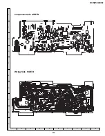
Page 94: ...106 DV NC55U C M A B C D E F G H I J 1 2 3 4 5 6 7 8 9 10 VTR DISPLAY PWB Component Side SIDE A Wiring Side SIDE A Component Side SIDE B Wiring Side SIDE B ...

Page 95: ...107 DV NC55U C M 10 11 12 13 14 15 16 17 18 19 A B C D E F G H I J 1 2 3 4 5 6 7 8 9 10 DVD DISPLAY PWB Component Side SIDE A Wiring Side SIDE A Component Side SIDE B Wiring Side SIDE B ...

Page 96: ...108 DV NC55U C M A B C D E F G H I J 1 2 3 4 5 6 7 8 9 10 AUDIO VIDEO PWB Component Side SIDE A Wiring Side SIDE A ...

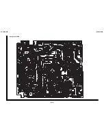
Page 97: ...109 DV NC55U C M 10 11 12 13 14 15 16 17 18 19 A B C D E F G H I J 1 2 3 4 5 6 7 8 9 10 Component Side SIDE B Wiring Side SIDE B ...

Page 98: ...110 DV NC55U C M A B C D E F G H I J 1 2 3 4 5 6 7 8 9 10 POWER PWB Component Side SIDE A Wiring Side SIDE A ...

Page 99: ...111 DV NC55U C M 10 11 12 13 14 15 16 17 18 19 A B C D E F G H I J 1 2 3 4 5 6 7 8 9 10 Component Side SIDE B Wiring Side SIDE B ...

Page 100: ...112 DV NC55U C M A B C D E F G H I J 1 2 3 4 5 6 7 8 9 10 INTERFACE PWB Component Side SIDE A Wiring Side SIDE A ...

Page 101: ...113 DV NC55U C M 10 11 12 13 14 15 16 17 18 19 A B C D E F G H I J 1 2 3 4 5 6 7 8 9 10 Component Side SIDE B Wiring Side SIDE B ...

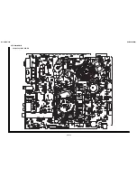
Page 102: ...1 2 3 4 5 6 7 8 9 10 11 12 13 14 15 16 17 18 19 20 A B C D E F G H I J DV NC55U C M DV NC55U C M 114 115 VTR MAIN PWB Component Side SIDE A ...

Page 103: ...1 2 3 4 5 6 7 8 9 10 11 12 13 14 15 16 17 18 19 20 A B C D E F G H I J DV NC55U C M DV NC55U C M 116 117 Wiring Side SIDE A ...

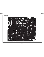
Page 104: ...1 2 3 4 5 6 7 8 9 10 11 12 13 14 15 16 17 18 19 20 A B C D E F G H I J DV NC55U C M DV NC55U C M 118 119 Component Side SIDE B ...

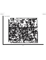
Page 105: ...1 2 3 4 5 6 7 8 9 10 11 12 13 14 15 16 17 18 19 20 A B C D E F G H I J DV NC55U C M DV NC55U C M 120 121 Wiring Side SIDE B ...

Page 106: ...122 DV NC55U C M A B C D E F G H I J 1 2 3 4 5 6 7 8 9 10 M E M O ...

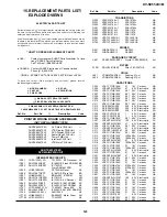
Page 107: ...trolytic AC C503 VCKYCY1CB104K 0 1 16V Ceramic AB C504 VCKYCY1CB104K 0 1 16V Ceramic AB C506 VCKYCY1CB104K 0 1 16V Ceramic AB C508 VCKYCY1CB104K 0 1 16V Ceramic AB C510 VCKYCY1CB104K 0 1 16V Ceramic AB C511 VCKYCY1CB104K 0 1 16V Ceramic AB C512 VCKYCY0JF105Z 1 6 3V Ceramic AB C515 VCKYCY1HB103K 0 01 50V Ceramic AA C516 VCKYCY1HB103K 0 01 50V Ceramic AA 15 REPLACEMENT PARTS LIST EXPLODED VIEWS ELEC...

Page 108: ... 16W Metal Oxide AA R528 VRS CY1JF103J 10k 1 16W Metal Oxide AA R529 VRS CY1JF472J 4 7k 1 16W Metal Oxide AA R530 VRS CY1JF103J 10k 1 16W Metal Oxide AA R531 VRS CY1JF472J 4 7k 1 16W Metal Oxide AA R532 VRS CY1JF103J 10k 1 16W Metal Oxide AA C517 VCKYCY1HB103K 0 01 50V Ceramic AA C519 VCKYCY1HB103K 0 01 50V Ceramic AA C520 VCKYCY1HB103K 0 01 50V Ceramic AA C521 VCKYCY1HB103K 0 01 50V Ceramic AA C5...

Page 109: ...n BLN 0076TA AC R812 RBLN 0076TAZZ Balun BLN 0076TA AC R813 RBLN 0076TAZZ Balun BLN 0076TA AC R533 VRS CY1JF103J 10k 1 16W Metal Oxide AA R534 VRS CY1JF103J 10k 1 16W Metal Oxide AA R535 VRS CY1JF103J 10k 1 16W Metal Oxide AA R536 VRS CY1JF000J 0 1 16W Metal Oxide AA R537 VRS CY1JF103J 10k 1 16W Metal Oxide AA R538 VRS CY1JF103J 10k 1 16W Metal Oxide AA R540 VRS CY1JF472J 4 7k 1 16W Metal Oxide AA...

Page 110: ...2SA1530AR AC Q2002 VS2SA1530ARS1 2SA1530AR AC Q2003 VS2SA1530ARS1 2SA1530AR AC R814 RBLN 0076TAZZ Balun BLN 0076TA AC R815 RBLN 0076TAZZ Balun BLN 0076TA AC R816 RBLN 0076TAZZ Balun BLN 0076TA AC R817 RBLN 0076TAZZ Balun BLN 0076TA AC R818 RBLN 0076TAZZ Balun BLN 0076TA AC R819 RBLN 0076TAZZ Balun BLN 0076TA AC MISCELLANEOUS PARTS CN201 QPLGN0964TAZZ Plug 9Pin AF CN301 QSOCN2336TAZZY Socket 23Pin ...

Page 111: ...e AA R2078 VRS CY1JF103J 10k 1 16W Metal Oxide AA R6060 VRS CY1JF561J 560 1 16W Metal Oxide AA R6061 VRS CY1JF561J 560 1 16W Metal Oxide AA R6062 VRS CY1JF823J 82k 1 16W Metal Oxide AA R6063 VRS CY1JF823J 82k 1 16W Metal Oxide AA R6064 VRS CY1JF823J 82k 1 16W Metal Oxide AA R6065 VRS CY1JF823J 82k 1 16W Metal Oxide AA R6066 VRS CY1JF823J 82k 1 16W Metal Oxide AA R6067 VRS CY1JF823J 82k 1 16W Metal...

Page 112: ... 5600p 50V Mylar AA å C910 VCKYPA1HB272K 2700p 50V Ceramic AA å C915 RC KZ0091GEZZ 2200p 250V Ceramic AC C9001 VCEA0A1VW477M 470 35V Electrolytic AB C9002 VCEAGA1EW337M 330 25V Electrolytic AC C9003 VCEA9M1HW226M 22 50V Electrolytic AB C9004 VCEA0A1AW228M 2200 10V Electrolytic AD C9006 VCEA0A1AW228M 2200 10V Electrolytic AD C9007 VCEA9M1CW107M 100 16V Electrolytic AB C9008 VCKYCY1HF103Z 0 01 50V C...

Page 113: ...19 AB FILTER FL8201 RFiLC0198GEZZ Filter FiLC0198GE AE COILS L6001 VP DF150K0000 Peaking 15µH AB L6101 VP MK100K0000 Peaking 10µH AB CAPACITORS C6003 VCKYCY1CB104K 0 1 16V Ceramic AB C6006 VCEA9M1CW106M 10 16V Electrolytic AB C6007 VCEA9M1CW106M 10 16V Electrolytic AB C6008 VCEA9M1CW106M 10 16V Electrolytic AB C6012 VCEA9M0JW227M 220 6 3V Electrolytic AB C6013 VCKYCY1CB104K 0 1 16V Ceramic AB C601...

Page 114: ...Q1251 VS2SA1530ARS1 2SA1530AR AC Q1302 VS2SD1306 E 1 2SD1306 E AC Q1306 VS2SA1530ARS1 2SA1530AR AC Q1501 VS2SC3052EF 1 2SC3052EF AC Q1602 VS2SC3203Y 1 2SC3203Y AB Q1603 VS2SC3052EF 1 2SC3052EF AC Q1604 VS2SC2712Y 1 2SC2712Y AB Q1605 VS2SC2712Y 1 2SC2712Y AB Q1606 VSKRA102S 1 KRA102S AA Q1651 VS2SD1306 E 1 2SD1306 E AC Q1652 VS2SD1306 E 1 2SD1306 E AC Q1653 VSKRA104S 1 KRA104S AA Q1654 VSKRC103S 1 ...

Page 115: ...Ceramic AA C1703 VCEA9M1HW105M 1 50V Electrolytic AB C1704 VCKYCY0JF105Z 1 6 3V Ceramic AB C1705 VCKYCY1EB103K 0 01 25V Ceramic AA C1706 VCKYCY1EB103K 0 01 25V Ceramic AA C1707 VCCCCY1HH150J 15p 50V Ceramic AA C1160 VCEA9M1HW225M 2 2 50V Electrolytic AB C1161 VCKYCY1CB104K 0 1 16V Ceramic AB C1162 VCKYCY1CB104K 0 1 16V Ceramic AB C1163 VCEA9M1CW106M 10 16V Electrolytic AB C1164 VCKYCY1CB104K 0 1 1...

Page 116: ...al Oxide AA R1657 VRS CY1JF101J 100 1 16W Metal Oxide AA R1658 VRS CY1JF223J 22k 1 16W Metal Oxide AA R1659 VRS CY1JF331J 330 1 16W Metal Oxide AA R1663 VRD RA2BE333J 33k 1 8W Carbon AA R1664 VRS CY1JF682J 6 8k 1 16W Metal Oxide AA R1665 VRS CY1JF473J 47k 1 16W Metal Oxide AA C1708 VCCCCY1HH150J 15p 50V Ceramic AA C1711 VCKYCY1HB102K 1000p 50V Ceramic AA C1712 VCKYCY1HB102K 1000p 50V Ceramic AA C1...

Page 117: ...Metal Oxide AA R1750 VRS CY1JF474J 470k 1 16W Metal Oxide AA R1751 VRD RA2BE123J 12k 1 8W Carbon AA DUNTK6068TEV2 VTR MAIN PWB UNIT Continued R1752 VRD RA2BE123J 12k 1 8W Carbon AA R1753 VRD RA2BE102J 1k 1 8W Carbon AA R1754 VRS CY1JF102J 1k 1 16W Metal Oxide AA R1756 VRS CY1JF102J 1k 1 16W Metal Oxide AA R1757 VRS CY1JF102J 1k 1 16W Metal Oxide AA R1759 VRD RA2BE561J 560 1 8W Carbon AA R1760 VRS ...

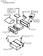
Page 118: ...iNS 4012AJZZ Operation Manual NC55U AM TiNS 4034AJZZ Operation Manual NC55C AM TLSTS0022TAZZ Ass List NC55C AB TGAN 3324AJZZ Guarantee Card NC55U AC SPAKC4620AJZZ Packing Case SPAKX1010AJZZ Packing Add SPAKP0209AJZZ Wrapping Paper SSAKA0001AJZZ Polyethylene Bag NC55U C TLABV0182AJZZ Bar Code Label TLABZ1717AJZZ Region 4 Label NC55M PACKING PARTS NOT REPLACEMENT ITEM MECHANISM PARTS DVD PART 401 CM...

Page 119: ...552 PREFL1011AJZZ Light Guide AE 553 QCNW 8022AJZZ FFC for Drum Motor AD 555 QCNW 8021AJZZ FFC for A C Head AD 556 QPWBF5243AJZZ A C Head PWB AE 557 QSOCN0696REZZ Socket 6 pin AB 558 RHEDT0036AJZZ Full Erase Head AM 559 RHEDU0089GEZZ A C Head Ass y AP 560 RMOTM1078GEZZ Loading Motor AP 561 RMOTN2067GEZZ Capstan D D Motor AY 562 RMOTP1151GEZZ Drum Drive Motor AT 563 DDRMW0030TEX1 Upper and Lower Dr...

Page 120: ...DUNTK6058TEV2 Audio Video PWB Unit 66 DUNTK6060TEV2 Interface PWB Unit 67 DUNTK6059TEV2 Power PWB Unit 68 DUNTK6054TE6D DVD Main PWB Unit 69 DUNTK6056TEV2 VTR Display PWB Unit 70 DUNTK6057TEV2 DVD Display PWB Unit 71 DUNTK6068TEV2 VTR Main PWB Unit 72 QCNW 8021AJZZ Connecting Cord AD 73 QCNW 8022AJZZ Connecting Cord AD 74 QCNW 8553AJZZ Connecting Cord AF å 75 QACCD3048AJZZ AC Cord AN 76 QCNW 8600A...

Page 121: ...ing Dry Coating Dry Coating Dry Coating Grease Grease Grease Grease Grease When touching the pickup wear an earth band to prevent breakage by static electricity å Caution 434 432 433 428 427 426 420 425 421 422 423 409 424 431 435 429 419 409 410 410 409 401 6 401 1 401 7 401 8 401 9 401 409 418 413 401 5 401 2 401 3 401 4 401 13 401 11 401 10 401 12 ...

Page 122: ...207 216 208 219 209 210 211 212 213 223 202 222 221 201 202 202 220 566 562 563 550 501 565 566 553 526 570 559 557 555 556 516 571 549 551 522 508 511 519 518 529 505 520 541 561 521 538 534 517 537 547 560 568 569 544 506 545 548 540 527 539 530 510 523 543 543 546 535 535 524 502 533 515 504 552 525 558 507 551 549 567 509 530 536 512 531 532 566 566 224 ...

Page 123: ... No Description Code Ref No Part No Description Code 139 DV NC55U C M CASSETTE HOUSING CONTROL EXPLODED VIEW A B C D E F G H 1 2 3 4 5 6 301 304 311 311 305 306 309 303 312 316 315 307 314 310 317 313 302 308 300 ...

Page 124: ... C A B A Z R Q P F X I G Y S R W P Q S A G I E D H A K T L K M D J C E O Y B F B X O U Z T L U V V W H H 25 46 51 24 1 52 25 25 93 87 36 40 76 66 53 90 25 44 64 35 54 46 32 22 48 28 67 89 53 25 71 32 58 91 3 80 59 70 39 30 42 90 69 88 88 78 79 72 46 73 84 52 55 48 83 68 77 45 56 74 55 63 61 65 24 81 41 52 29 86 57 85 75 82 62 40 58 50 49 17 ...

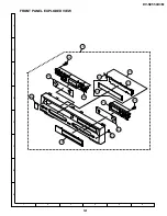
Page 125: ...Ref No Part No Description Code Ref No Part No Description Code 141 DV NC55U C M FRONT PANEL EXPLODED VIEW A B C D E F G H 1 2 3 4 5 6 616 601 607 605 609 614 612 617 616 610 608 618 606 615 ...

Page 126: ...d TLSTS0022TAZZ DV NC55C Ass List TiNS 4012AJZZ DV NC55U TiNS 4034AJZZ DV NC55C Operation Manual RRMCG1293AJSA Remote Control unit SSAKA0001AJZZ DV NC55U C Polyethylene Bag QCNW 8387AJZZ 75 Ohm Coaxial Cable QCNW 8549AJZZ VIDEO AUDIO Cable SPAKX1010AJZZ Packing Add TLABZ1717AJZZ DV NC55M Region 4 Label TLABV0182AJZZ Bar Code Label TLABZ1717AJZZ DV NC55M Region 4 Label SPAKX1010AJZZ Packing Add ...

Page 127: ...Ref No Part No Description Code Ref No Part No Description Code 143 DV NC55U C M ...

Page 128: ...Tochigi 329 2193 Japan COPYRIGHT 2001 BY SHARP CORPORATION ALL RIGHTS RESERVED No part of this publication may be reproduced stored in a retrieval system or transmitted in any form or by any means electronic mechanical photocopying recording or otherwise without prior written permission of the publisher D Japan P SMM TQ1139 S Jul 2001 Printed in JAPAN SA DS ...

Reviews: