FO-77U
UX-66U
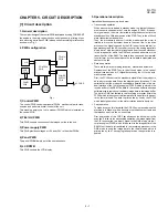
[2] Circuit description of control PWB
1. General description
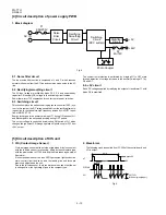
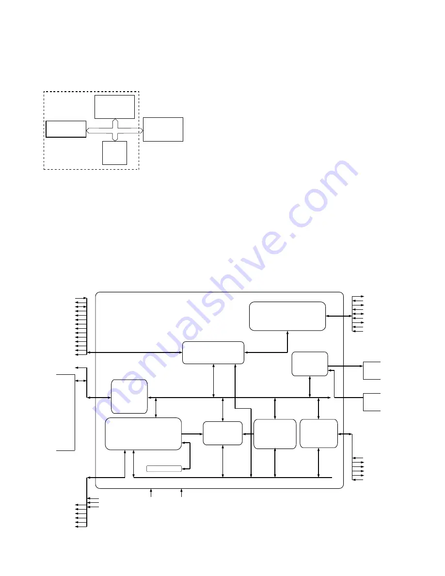
Fig. 2 shows the functional blocks of the control PWB, which is com-
posed of 4 blocks.
Fig. 2 Control PWB functional block diagram
2. Description of each block
(1) Main control block
The main control block is composed of CONEXANT 1 chip fax engine
(FC200), ROM (1Mbit), SRAM (256kbit) and Modem (FM209).
Devices are connected to the bus to control the whole unit.
1) FC200 (IC2) : pin-144 QFP (FAX ENGINE)
2) FM209 (IC4) : pin-128 QFP (MODEM)
The FAX ENGINE Integrated Facsimile Controllers.
FC200, contains an internal 8 bit microprocessor with an external 16
Mbyte address space and dedicated circuitry optimized for facsimile
image processing and facsimile machine control and monitoring.
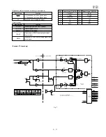
3) 27E010 (IC5): pin-32 DIP (ROM)
ROM of 1 Mbit equipped with software for the main CPU.
4) W24258S-70LE (IC3): pin-28 SOP (SRAM)
Line memory for the main CPU system RAM area and coding/decoding
process. Used as the transmission buffer.
Memory of recorded data such as daily report and auto dials. When the
power is turned off, this memory is backed up by the lithium battery.
Fig. 3
5 – 2
(1) FAX ENGINE
(3) ROM
(2) MODEM
(4) SRAM
MAIN CONTROL BLOCK
MODEM BLOCK
MC24 CPU CONTROL IF
MC24 MEGACELL(8BIT DATA,24BIT ADDRESS)
WATCHDOG TIMER
REAL TIME CLOCK
CRYSTAL OSCILLATOR
BATTERY BACK-UP CIRCUIT
INTERRUPT CONTROLLER
BUS INTERFACE
DRAM CONTROL
INTERNAL & EXTERNAL BUS CONTROL
INTERNAL & EXTERNAL DECODE
DMA CONTROLLER
OPERATOR PANEL IF
32 KEYS
8 LEDS
LCD MODULE
MOTOR POWER
CONTROL RINGER
SYNC SERIF 1
THERMAL PRINTER IF
5 ms LINE TIME
A4/B4 LINES
TPH ADC
4 STROBE TPH
LATCHLESS TPH
EXTEMAL DMA I/F
T.4/T.6 CODEC
MH,MR,MMR
HARDWARE,ALTERNATE
COMPRESSION &
DECOMPRESSION
BI-LEVEL RESOLUTION
CONVERSION
PROGRAMMABLE
REDUCTION &
EXPANSION
2.6kBYTE VIDEO RAM
SCANNER CONTROL & VIDEO PROCESSING
8-BIT PADC
CCD/CIS SCANNER
5 ms,A4/B4 LINES
SHADING CORRECTION(1:1,1:8)
DITHERING
MULTILEVEL B4-A4 REDUCTION
ERROR DIFFUSION
MTF
GENERAL I/O
TONE/ALTTONE
GPIO
CALLING PARTY
CONTROL
AUTOBAUD
SYNC-ASYNC SASIF
SYNC SERIF 2
FLASH MEMORY IF
AUTOBAUD
CPU BUS
INTERNAL CPU BUS
EXTERNAL CPU BUS
DMA BUS
WRPROTN
TSTCLK
DEBUGN
RESETN
XIN
XOUT
PWRDWNN
BATRSTN
SYSCLK
SEE
"OPIF
OUTPUTS"
BELOW
SEE
"OPIF
INPUTS"
BELOW
THADIN
PDAT
PLAT
STRB[3:0]
STRBPOL
PCLK
PWR/GND
TEST
OPIF INPUTS
OPI[0]/GPIO[21]/SSRXD1
OPI[1]/GPIO[22]/SSSTAT1
OPI[2]/GPIO[23]/SSCLK1
OPI[3]/GPIO[24]
OPIF OUTPUTS
LEDCTL/GPO[16]
LCDCS/GPO[17]
OPO[0]/GPO[8]/SINPWR CTRL
OPO[1]/GPO[9]/PMPWR CTRL
OPO[2]/GPO[10]/RINGER
OPO[3]/GPO[11]
OPO[4]/GPO[12]/SSTXD1
OPO[5]/GPO[13]
OPO[6]/GPO[14]
OPO[7]/GPO[15]
ROMCSN
MCSN
SYNC
REGDMA
WAITN
RASN
CASN[1:0]
DWRN
CSN[1:0]
WRN
RDN
D[7:0]
A[23:0]
MIRQN
TONE
VIN
CLK1
CLK1N
CLK2
VIDCTL0/FCS1N
VIDCTL1/FCS2N
START
–VREF
+VREF
GPIO[0]
GPIO[1]/SASTXD
GPIO[2]/SASRXD
GPIO[3]/SASCLK
GPIO[4]/CPCIN
GPIO[5]/SSCLK2
GPIO[6]/SSTXD2
GPIO[7]/SSRXD2
GPIO[8]/FWRN
GPIO[9]/FRDN
GPIO[10]/SSSTAT2
GPIO[11]/BE/SERINP
GPIO[12]/CS2N
GPIO[13]/CS3N
GPIO[14]/CS4N
GPIO[15]/CS5N
GPIO[16]/IRQ8
GPIO[17]/IRQ5N
GPIO[18]/IRQ9N
GPIO[19]/RDY/SEROUT
GPIO[20]/ALTTONE
SM[3:0]/GPO[7:4]
PM[3:0]/GPO[3:0]
Summary of Contents for FO-77
Page 65: ...FO 77U UX 66U Control PWB parts layout Top side 6 7 ...
Page 66: ...FO 77U UX 66U Control PWB parts layout Bottom side 6 8 ...
Page 69: ...FO 77U UX 66U TEL LIU PWB parts layout Top side 6 11 ...
Page 70: ...FO 77U UX 66U 6 12 TEL LIU PWB parts layout Bottom side ...
Page 72: ...FO 77U UX 66U Power supply PWB parts layout 6 14 RDENT2142XHZZ F2 ...
Page 97: ...FO 77U UX 66U 14 M E M O ...

