– 24 –
GX-CD1200W
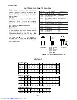
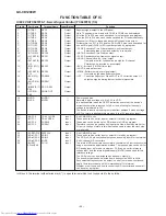
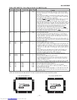
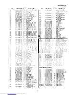
IC802 VHiTC9457F0-1: Servo/Signal Control (TC9457F0) (1/4)
1*
(OT5)S1
SEG1
Output
Segment signal output to the LCD panel.
2
(OT6)S2
SEG2
Output
Up to 72 segments in a matrix with COM1 to COM4 can be displayed.
3
(OT7)S3
SEG3
Output
All of the S1 to S18 pins can be switched for output ports by a program.
4
(OT8)S4
SEG4
Output
Also, the S15 to S18 pins each can be switched for I/O ports individually.
5
(OT9)S5
SEG5
Output
When set for I/O ports, these pins become Nch open-drain output.
6*
(OT10)S6
SEG6
Output
Furthermore, the S11 to S14 and the P8-0 to P8-3 pins can be switched for
7*
(OT11)S7
SEG7
Output
use as CD signal (CLCK to IPF) input/output pins by a program.
8*
(OT12)S8
SEG8
Output
• CLCK: Subcodes P thru W data readout clock input/output.
9*
(OT13)S9
SEG9
Output
Selected between input and output by a command.
10*
(OT14)S10
SEG10
Output
• DATA: Subcodes P thru W data output.
11*
(CLCK/OT15)
SEG11
Output
• SFSY: Playback system frame sync signal output.
S11
• LRCK: Channel clock (44.1kHz) output.
12*
(DATA/OT16)
SEG12
Output
It outputs a low for L channel and a high for R channel.
S12
Polarity can be inverted by a command.
13*
(SFSY/OT17)
SEG13
Output
• BCK : Bit clock (1.4122MHz) output.
S13
• AOUT: Audio data output.
14*
(LRCK/OT18)
SEG14
Output
• MBOV: Buffer memory-over signal output.
S14
It outputs a high when buffer overflows.
15
(BCK/S15)
CDSEL0
Output
• IPF : Correction flag output. When AOUT is C2 correction output, it
P8-0
outputs a high indicating that correction is impossible.
16
(AOUT/S16)
CDSEL1
Output
P8-1
17
(MBOV/S17)
CD LID SW
Output
P8-2
18
(IPF/S18)
DOOR OUT
Output
P8-3
19
MVDD
MVDD1
—
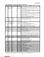
Power supply pins.
20
MVSS
MVSS1
—
Normally, apply a voltage of 4.5 to 5.5V to VDD.
In a backup state (when the CKSTP instruction executed), the device's
current consumption is reduced to 1
µ
A or less, allowing for the supply
voltage to be lowered to 2.0V.
The device is reset and the program starts from address 0 when a voltage
of 2.7V or more is applied to this pin when it is at 0V (power-on reset).
21*
(K0)P1-0
TRAY CLOSE
Input
4-bit CMOS I/O ports.
22*
(K1)P1-1
TRAY OPEN
Input
These ports can be set for input or output bit for bit by a program.
23
(K2)P1-2
PUSEL0
Input
These pins can be pulled up to VDD or down to GND by program.
24
(K3)P1-3
PUSEL1
Input
Therefore, they can be used as key input pins. Also, when they are set for
I/O port, a change of state in this input can be used to clear the clock stop
or wait mode.
25
(DCREF)P3-0
DISPLAY
Input
5-bit CMOS I/O ports.
26
(ADin1)P3-1
ADIN1
Input
These ports can be set for input or output bit for bit by a program.
27
(ADin2)P3-2
ADIN2
Input
The P3-0 to P4-0 pins serve dual purposes as analog inputs for the internal
28
(ADin3)P3-3
MUTE
Input
6-bit 4-channel A/D converters.
29
(BUZR/
PU IN
Input
The internal A/D converters can complete conversion in 6 instruction cycles
ADin4)P4-0
using a successive approximation method. The required pins can be set for
A/D analog input bit for bit by a program. P3-0 can be set for reference
voltage input, and the internal power supply (MVDD) can be used for this
reference voltage.
The P4-0 pin serves dual purposes as a buzzer output pin.
The buzzer output can be selected from 8 frequencies, 0.625 to 3kHz.
Each selected frequency can be output in one of four modes: continuous,
single, 10Hz intermittent, and 10Hz intermittent at 1Hz interval.
Whether or not to use and how to control the A/D converter and buzzer all
can be set by a program.
Port Name
Terminal Name
Pin No.
Input/Output
In this unit, the terminal with asterisk mark (*) is open terminal which is not connected to the outside.
Function
FUNCTION TABLE OF IC
Summary of Contents for GX-CD1200W BK
Page 28: ... 28 GX CD1200W M E M O ...
Page 38: ...GX CD1200W M E M O 9 ...
Page 39: ...GX CD1200W M E M O 10 ...

