– 25 –
GX-CD1200W
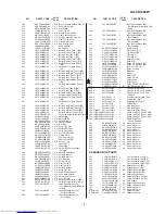
IC802 VHiTC9457F0-1: Servo/Signal Control (TC9457F0) (2/4)
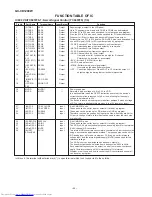
30
(S12)P4-1
PUSEL2
Input
3-bit CMOS I/O ports.
31*
(SO/S11/
NC
Input/Output
These ports can be set for input or output bit for bit by a program.
SDA)P4-2
These pins serve dual purposes as input or output pins for the serial
32*
(SCK/SCL)
NC
Input/Output
interface circuit (SIO).
P4-3
The SIO is a 2-wire/3-wire compatible serial interface. 4 or 8 bits of serial
data, beginning with the MSB or LSB, are serially output from the SO/SDA,
pin at each clock edge on the SCK/SCL pin, and the data on S11 or S12
pin is serially input to the device.
The serial clock (SCK/SCL) allows selection between the internal (450/225/
150/75 kHz) and external sources and a selection of the active edge, rise or
fall. Moreover, since the clock and data can be output via Nch open-drain
outputs, various, device controls and communication between controllers
can be greatly facilitated.
When an SIO interrupt is enabled, an interrupt is generated at completion
of SIO execution and the program jumps to address 4.
All inputs to SIO contain a Schmitt trigger circuit.
33
TEST0
TEST0
Input
Test mode control input pins.
34
TEST1
TEST1
Input
The test mode is selected when these pins are set high and normal
35
TEST2
TEST2
Input
operation is selected when they are low.
36
TEST3
TEST3
Input
37
TEST4
TEST4
Input
38
TEST5
TEST5
Input
39*
(OT19)/HSO
/HSO
Output
CD control output pins.
40*
(OT20)SPCK SPCK
Output
• /HSO: Playback speed mode output.
41*
(OT21)SPDA SPDA
Output
High = normal speed; Low = double speed.
42*
(OT22)COFS COFS
Output
• SPCK: Processor status signal readout clock output (176.4kHz)
• SPDA: Processor status signal output.
• COFS: Correction system frame clock output (7.35kHz)
These pins can be switched for output ports by a program.
43*
DOUT
DOUT
Input/Output
Digital output pin.
44*
SBSY
SBSY
Input/Output
Subcode block sync output pin. It outputs a high at the S1 position when
subcode sync is detected.
45*
SBOK
SBOK
Input/Output
Subcode Q data CRCC determination result output pin. It outputs a high
when CRCC check is found OK.
46
VDD
VDD1
Input/Output
CD unit's digital block power supply pins.
47
VSS
VSS1
Input/Output
Normally, apply 5V to VDD.
When not using a CD (CD off), this power supply can be turned off, with
only the controller power supply kept active, so that the controller alone is
operating. In this case, the CD off bit must be set to 1. When this bit is set
to 1, pins 11 through 18 and pins 39 through 42 all are changed for output
ports if they have been set for CD control signal input/output pins.
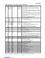
48
P2VREF
P2VREF
Input/Output
PLL block-2 VREF pin.
49
PDO
PDO
Input/Output
This pin outputs a phase error between EFM and PLCK signals.
50
TMAX
TMAX
Input/Output
TMAX detection result output pin.
Selected by command bit TMPS.
Longer than preset period: Outputs P2VREF.
Shorter than preset period: Low level (Vss).
Within preset period: High impedance.
51
LPFN
LPFN
Input/Output
Inverted input of low-pass filter amp.
52
LPFO
LPFO
Input/Output
Output of low-pass filter amp.
53
PVREF
PVREF
Input/Output
PLL block VREF pin.
54
VCOF
VCOF
Input/Output
VCO filter pin.
55
AVSS
AVSS
Input/Output
Analog block ground pin.
56
SLCO
SLCO
Input/Output
DAC output pin for data slice level generation.
57
RFI
RFI
Input/Output
RF signal input pin.
58
AVDD
AVDD
Input/Output
Analog block power supply pin.
59
RFCT
RFCT
Input/Output
RFRP signal center level input pin.
60
RFZI
RFZI
Input/Output
RFRP zero-cross input pin.
61
RFRP
RFRP
Input/Output
RF ripple signal input pin.
62
FEI
FEI
Input/Output
Focus error signal input pin.
Port Name
Terminal Name
Pin No.
Input/Output
In this unit, the terminal with asterisk mark (*) is open terminal which is not connected to the outside.
Function
Summary of Contents for GX-CD1200W BK
Page 28: ... 28 GX CD1200W M E M O ...
Page 38: ...GX CD1200W M E M O 9 ...
Page 39: ...GX CD1200W M E M O 10 ...


