– 26 –
GX-CD1200W
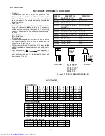
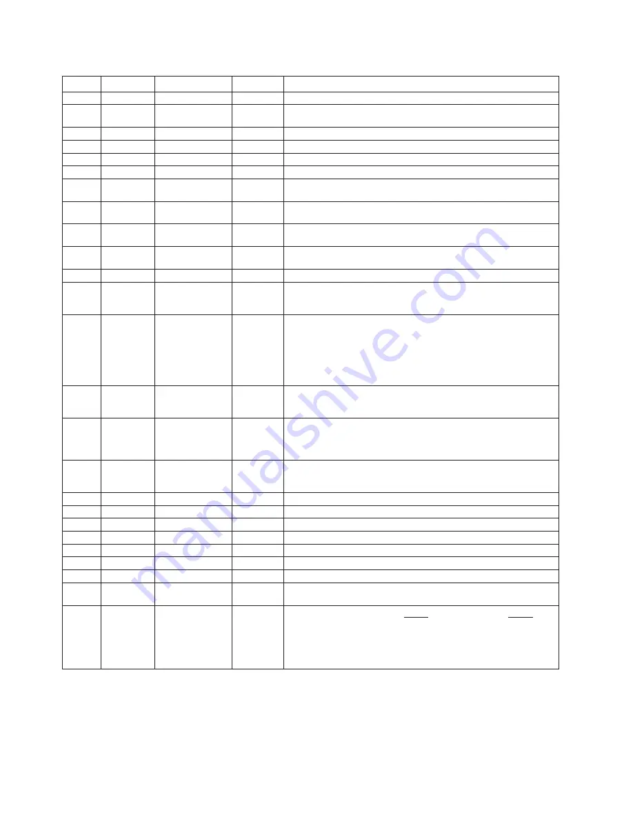
IC802 VHiTC9457F0-1: Servo/Signal Control (TC9457F0) (3/4)
63
SBAD
SBAD
Input/Output
Subbeam add signal input pin.
64
TEI
TEI
Input/Output
Tracking error input pin.
This input is read when tracking servo is on.
65
TEZI
TEZI
Input/Output
Tracking error zero-cross input pin.
66
FOO
FOO
Input/Output
Focus equalizer output pin.
67
TRO
TRO
Input/Output
Tracking equalizer output pin.
68
VREF
VREF
Input/Output
Analog reference power supply pin.
69
RFGC
RFGC
Input/Output
RF amplitude adjusting control signal output pin. It outputs 3-level PWM
signals. (PWM carrier = 88.2kHz)
70
TEBC
TEBC
Input/Output
Tracking balance control signal output pin. It outputs 3-level PWM signals.
(PWM carrier = 88.2kHz)
71
FMO
FMO
Input/Output
Focus equalizer output pin. It outputs 3-level PWM signals.
(PWM carrier = 88.2kHz)
72
DMO
DMO
Input/Output
Disc equalizer output pin. It outputs 3-level PWM signals.
(PWM carrier = DSP block 88.2kHz, synchronized to PXO)
73
2VREF
2VREF
Input/Output
Analog reference power supply pin. (2 x VREF)
74
SEL
SEL
Input/Output
APC circuit on/off signal output pin.
When laser is on, this pin goes to a high-impedance state when UHS = low
and outputs a high when UHS = high
75
VDD
VDD2
Input/Output
CD unit's digital block power supply pins.
76
VDD
VSS2
Input/Output
Normally, apply 5V to VDD.
When not using a CD (CD off), this power supply can be turned off, with
only the controller power supply kept active, so that the controller alone is
operating. In this case, the CD off bit must be set to 1. When this bit is set
to 1, pins 11 through 18 and pins 39 through 42 all are changed for output
ports if they have been set for CD control signal input/output pins.
77
XVSS
XVSS
Input/Output
CD's crystal oscillator power supply pins.
Normally, connect these pins to the power supply lines that are used in
common for the VDD and VSS pins.
78
XI
XI
Input/Output
CD's crystal oscillator input/output pins.
79
XO
XO
Input/Output
Normally, connect 16.934MHz here. This clock is used as the system clock
for the CD. After a system reset, it also is used as the system clock on the
controller side.
80
XVDD
XVDD
Input/Output
CD's crystal oscillator input/output pins.
Normally, connect these pins to the power supply lines that are used in
common for the VDD and VSS pins.
81
DVSR
DVSR
Input/Output
R-channel D/A converter unit ground pin.
82
RO
RO
Input/Output
R-channel data forward output pin.
83
DVRR
DVRR
Input/Output
R-channel reference voltage pin.
84
DVDD
DVDD
Input/Output
D/A converter unit power supply pin.
85
DVRL
DVRL
Input/Output
L-channel reference voltage pin.
86
LO
LO
Input/Output
L-channel data forward output pin.
87
DVSL
DVSL
Input/Output
L-channel D/A converter unit ground pin.
88
NC
NC
Input/Output
NC pins. Normally, connect these pins to ground or leave them open.
89*
NC/VPP
NC
Input/Output
90
/RST
RESET
Input
Device's system reset signal input pin.
The device remains reset while RESET is held low and when RESET is
released back high, the CD unit becomes operational and the program
starts from address 0. Normally, a system reset is asserted when a voltage
of 2.7V or more is applied to VDD when it is at 0V (power-on reset).
Therefore, this pin must be pulled high when used for this purpose.
Port Name
Terminal Name
Pin No.
Input/Output
In this unit, the terminal with asterisk mark (*) is open terminal which is not connected to the outside.
Function
Summary of Contents for GX-CD1200W BK
Page 28: ... 28 GX CD1200W M E M O ...
Page 38: ...GX CD1200W M E M O 9 ...
Page 39: ...GX CD1200W M E M O 10 ...


