– 27 –
GX-CD1200W
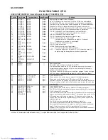
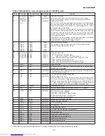
IC802 VHiTC9457F0-1: Servo/Signal Control (TC9457F0) (4/4)
91
/HOLD
HOLD
Input
This pin is used to input a signal that requests or clears the hold mode.
Normally, use this pin for CD mode select signal input or battery detection
signal input.
There are two hold modes: clock stop mode (crystal oscillator turned off)
and a wait mode (CPU stopped). These modes are entered by executing
the CKSTP and WAIT instructions, respectively.
The clock stop mode can be requested by a programmed input: low level
detection on HOLD pin or forced execution, and can be cleared by
detecting a high on the HOLD pin or a change of state in its input signal.
When the CKSTP instruction is executed, the clock generator and the CPU
stop operating and the device is placed in a memory backup state. During
this state, the device's current consumption is reduced to 1
µ
A or less.
At the same time, the display output and CMOS output ports are
automatically set low, and the Nch open-drain outputs are turned off.
The wait mode is executed regardles of the input state on the HOLD pin,
with the device's current consumption reduced.
This mode is cleared by a change of state in the HOLD input.
92
INTR
REMO-IN
Input
External interrupt input pin.
When the interrupt facility is enabled and a pulse of 1.11 to 2.22
µ
s in
duration is applied to this pin, an interrupt is generated and the program
jumps to address 1. Input logic and the active edge (rise or fall) can be
selected for each interrupt input.
Also, the internal 8-bit time clock can be chosen for this interrupt input, in
which case it is possible to count pulses or generate an interrupt at a given
pulse count (address 3).
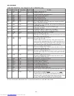
93*
MXO
MXO
—
Crystal oscillator pins for the controller.
94*
MXI
MXI
—
The oscillator clock is used as the timebase for the clock facility or as the
controller's system clock. Connect a 4.5MHz or 75kHz crystal resonator to
the MXO and MXI pins. Since these pins do not contain internal feedback
resistors, etc, an amp resistor or output resistor must be added external to
the chip.
When using the clock generated by the CD unit's crystal oscillator for
clocking the entire device operation, fix the MXI pin to the GND level.
Oscillation is stopped by executing a CKSTP instruction.
Select the crystal oscillator and control its operation by a program.
95
MVSS
MVSS
—
Power supply pins.
96
MVDD
MVDD
—
Normally, apply a voltage of 4.5 to 5.5V to VDD.
In a backup state (when the CKSTP instruction executed), the device's
current consumption is reduced to 1
µ
A or less, allowing for the supply
voltage to be lowered to 2.0V.
The device is reset and the program starts from address 0 when a voltage
of 2.7V or more is applied to this pin when it is at 0V (power-on reset).
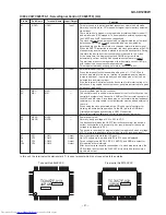
97
OT1
COM1
Output
Common signal outputs to the LCD panel.
98
OT2
COM2
Output
Up to 72 segments in a matrix with S1 to S18 can be displayed.
99
OT3
COM3
Output
Three voltage levels MVDD, VEE (1/2 MVDD), and GND are output for
100
OT4
COM4
Output
83Hz period at 2ms intervals.
After a system reset and after deassertion of a clock stop instruction, the
VEE voltage is output and the DISP OFF bit is set to 0 before common
signals are output.
Port Name
Terminal Name
Pin No.
Input/Output
In this unit, the terminal with asterisk mark (*) is open terminal which is not connected to the outside.
Function
TC9457F-013
JAPAN
TC7457F-022
JAPAN
To serial No.006XXXXX
From serial No.007XXXXX
Summary of Contents for GX-CD1200W BK
Page 28: ... 28 GX CD1200W M E M O ...
Page 38: ...GX CD1200W M E M O 9 ...
Page 39: ...GX CD1200W M E M O 10 ...


