background image

GX-CD1200W

– 4 –

DISASSEMBLY

Caution on Disassembly
Follow the below-mentioned notes when disassembling
the unit and reassembling it, to keep it safe and ensure
excellent performance:
1. Take cassette tape  out of the unit.
2. Be sure to remove the power supply plug from the wall

outlet before starting to disassemble the unit and remove
the batteries from the unit.

3. Take off nylon bands or wire holders where they need

to be removed when disassembling the unit. After
servicing the unit, be sure to rearrange the leads where
they were before disassembling.

4. Take sufficient care on static electricity of integrated

circuits and other circuits when servicing.

STEP

REMOVAL

PROCEDURE

FIGURE

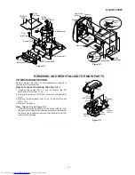
1

Front Cabinet/

1. Battery Compartment Lid.

4-1

Rear Cabinet

................................. (A1)x1

2. Screw ................... (A2)x5
3. Screw ................... (A3)x3
4. Socket .................. (A4)x1

2

CD Player Unit

1. Screw ................... (B1)x2

4-2

2.Socket ................... (B2)x1

3

Main PWB/

1. Knob ..................... (C1)x1

4-3

Graphic Equalizer 2. Socket .................. (C2)x3
PWB/

3. Screw ................... (C3)x5

Volume PWB/

4. Screw ................... (C4)x2

Fine Tuning PWB 5. Mic ....................... (C5)x1

4

Tape mechanism 1. Open the cassette holder.

4-3

2. Screw ................... (D1)x6

5

Power PWB/

1. Screw ................... (E1)x3

4-4

Terminal A PWB/ 2. Screw ................... (E2)x2
Terminal B PWB

3. Bracket ................. (E3)x1

4. Screw ................... (E4)x2
5. Hook ..................... (E5)x2

6

CD Servo PWB/

1. Screw ................... (F1)x7

5-1

CD Control PWB/ 2. Socket .................. (F2)x3

7

CD Mechanism

1. Screw ................... (G1)x1

5-1

Figure 4-4

Figure 4-2

Figure 4-1

Figure 4-3

STEP

REMOVAL

PROCEDURE

FIGURE

1

Speaker

1. Screw ................... (H1)x5

5-2

2. Front Panel .......... (H2)x1
3. Screw ................... (H3)x4

MAIN UNIT

SPEAKER UNIT

(A1)x1

(A4)x1

Front

Cabinet

Rear

Cabinet

(A2)x1

ø3x6mm

(A2)x1

ø3x6mm

(A3)x3

ø3x20mm

(A2)x3

ø3x6mm

Main PWB

(B1)x2
ø3x10mm

(B2)x1

Front Cabinet

CD SERVO PWB

CD Player Unit

Front Cabinet

Washer

Nat

(C1)x1

(C4)x2
ø3x10mm

(D1)x4
ø3x10mm

(C3)x5
ø3x10mm

(D1)x2
ø3x10mm

Tape
Mechanism

(C5)x1

(C2)x3

Cassette
Holder
(Left/Right)

Open

Fine Tuning 

PWB

Volume
PWB

Graphic
Equalizer 
PWB

Main PWB

Rear Cabinet

(E1)x3
ø3x10mm

(E2)x2
ø4x16mm

(E4)x2
ø3x10mm

Power 
Transeformer 

Voltage Selector

AC Socket

(E3)x1

Power

PWB

Terminal B
PWB

Terminal A
PWB

(E5)x2

Summary of Contents for GX-CD1200W BK

Page 1: ...wer PMPO 200 W Total AC operation MPO 50 W 25 W 25 W AC operation RMS 25 W 12 5 W 12 5 W DC operation 10 T H D Input terminal Mixing microphone monaural 600 ohms Output terminal Headphones 16 50 ohms recommended 32 ohms Dimensions Width 300 mm 11 13 16 Height 262 mm 9 1 2 Depth 220 mm 8 11 16 Weight 4 1 kg 9 1 lbs without batteries Compact disc player Type Compact disc Signal readout Non contact 3...

Page 2: ...te 6 Adjust the dial pointer so that its stopper becomes the Figure 2 2 position Adjust the engagement of the pointer gear and the tuner gear to get the minimum space between the PWB and the stopper This position is the 0 point 7 Screw up the PWB and the dial pointer guide Figure 2 2 Fine Tuning PWB Dial Pointer 211 0 Point Dial Pointer 211 Tuner Gear Tuning Knob Front Cabinet PWB Dial Pointer Gui...

Page 3: ...tch 24 Band Selector Switch 25 Dubbing Speed Built in Microphone FM Mode Switch 26 TAPE 2 Cassette Compartment 27 TAPE 1 Record Button 28 TAPE 1 Play Button 29 TAPE 1 Rewind Button 30 TAPE 1 Fast Forward Button 31 TAPE 1 Stop Eject Button 32 TAPE 1 Pause Button 33 TAPE 2 Reverse Mode Switch 34 TAPE 2 Play Button 35 TAPE 2 Fast Wind Buttons 36 TAPE 2 Stop Eject Button 37 TAPE 2 Direction Switch 38 ...

Page 4: ... Graphic Equalizer 2 Socket C2 x3 PWB 3 Screw C3 x5 Volume PWB 4 Screw C4 x2 Fine Tuning PWB 5 Mic C5 x1 4 Tape mechanism 1 Open the cassette holder 4 3 2 Screw D1 x6 5 Power PWB 1 Screw E1 x3 4 4 Terminal A PWB 2 Screw E2 x2 Terminal B PWB 3 Bracket E3 x1 4 Screw E4 x2 5 Hook E5 x2 6 CD Servo PWB 1 Screw F1 x7 5 1 CD Control PWB 2 Socket F2 x3 7 CD Mechanism 1 Screw G1 x1 5 1 Figure 4 4 Figure 4 ...

Page 5: ...w to remove the pickup See Fig 5 3 1 Remove the hooks A1 x 2 pcs to remove the CD Mechanism Cover A2 x1 pc 2 Remove the screws A3 x 2 pcs to remove the shaft A4 x1 pc 3 Remove the stop washer A5 x1 pc to remove the gear A6 x 1 pc 4 Remove the pickup REMOVING AND REINSTALLING THE MAIN PARTS Figure 5 3 Note Figure 5 1 and Figure 5 3 After removing the connector for the optical pick up from the conne...

Page 6: ...ig 6 1 and then extract the erase head upward 3 Remove the screws B1 x 2 pcs to remove the playback head Note After replacing the heads and performing the azimuth adjust ment be sure to apply screw lock How to remove the pinch roller See Fig 6 3 1 Carefully bend the pinch roller pawl in the direction of the arrow A and remove the pinch roller C1 upwards How to remove the motor See Fig 6 4 1 Remove...

Page 7: ...ter preparing the test circuit shown in Fig 7 connect the Pin 13 Pin 21 and ground of the IC2 with the test circuit and measure the value FM IF RF Specified Value Adjusting Point Test Stage FM IF L9 Input FM Antenna FM Detection L10 Output Pin 9 of IC2 FM Band fL L1 Input Antenna Coverage fH TC1 Output Headphone Socket FM Tracking fL 88 0 MHz L2 Load resistance fH 108 MHz TC2 32 ohms Instrument Co...

Page 8: ...L10 CNP501 SPEAKER TERMINALS 1 24 12 SW1 TRACKING fH TC1 TC2 TC3 TC4 MW TRACKING fH MW BAND COVERAGE fH FM TRACKING fH FM BAND COVERAGE fH fL SW2 TRACKING fH fL L4 L3 SW1 TRACKING fL MW TRACKING fL FM TRACKING fL AM IF FM IF FM DETECTION VCO SW1 BAND COVERAGE fH fL SW2 BAND COVERAGE fH fL MW BAND COVERAGE fL TAPE SPEED MAIN PWB 9 21 13 MAIN PWB ...

Page 9: ... After connecting of the 10kΩ resistor between IC802 27 pin and GND and holding down the PLAY button move the FUNCTION POWER switch to CD Start Display LCD MODE 1 Remove the front cabinet according to the disassembly method 2 Short the TP of the Figure 9 to turn on the CD LID SW 810 3 While holding down the PLAY button move the FUNCTION POWER switch to CD 4 Open the CD LID and press the PLAY butto...

Page 10: ... CF2 FM IF BI804 R152 4 7K R166 560 D163 DS1SS133 R168 10K R169 10K Q153 KTC3199 GR MIC AMP R165 10K C157 1 50 C156 100 10 R154 560 R151 2 2K C151 0 33 50 C154 47 10 R161 1M C155 10 16 Q156 KTC3199 GR LINE AMP R173 10K C152 10 16 C137 0 0015 ML L103 22mH R135 10K C131 120P R101 100 R121 10K C107 330P C113 4 7 50 C109 47 10 R109 6 8K R105 180K C111 0 015 ML R107 10K C103 470P C105 330P C101 470P C1...

Page 11: ...R435 2 2 C425 0 1 ML R433 2 2 IC402 LA4663 POWER AMP R412 10K R413 10K R416 3 3K C410 1 50 R418 22K C408 4 7 50 R419 3 3K R417 22K C411 47 10 R407 12K R409 12K R442 15K R441 15K R425 1K C424 47 25 C423 10 16 C420 4 7 50 C419 4 7 50 Q404 KTC3199 GR POWER MUTE Q403 KTC3199 GR POWER MUTE R426 1K R428 4 7K R427 4 7K C418 22 16 R429 100K VR401 50K B VR401 50K B C416 0 15 ML C414 0 001 ML C413 0 001 ML ...

Page 12: ...D VR PD G B SP SP SL SL TRO FOO DMO FMO FC FC TR TR GND PD VR LD SLT SLT FM FM DM DM 7 6 5 4 3 2 1 N C VCC VREF CD RES REG IN REG OUT VIN4 VIN3 VIN2 GND GND GND GND GND GND VG4 VG3 VG2 VO4 VO4 VO3 VO3 VO2 VO2 VO1 VO1 VG1 VIN1 MT VCC VCC FNI FPI TPI TNI MDI LDO SEL TEB 2VRO TEN TEO RFN GND RFO AGCI RFGC RFGO RFIS RFRP VRO FEN FEO SBAD 7 6 5 4 3 2 1 M 1 2 3 4 5 6 7 8 1 2 3 4 5 6 7 8 6 5 4 3 2 1 6 5 ...

Page 13: ...NTROL PWB C2 2 4 3 1 6 5 SEG9 PUSEL2 P3 0 P1 0 MVSS1 MVDD1 CDSEL0 SEG1 COM1 HOLD INTR MXO MXI MVSS MVDD RESET DVSL LO DVRR DVDD DVRL RO DVSR TEST0 SPCK DOUT VDD1 TMAX LPFN LPFO PVREF VCOF AVSS SLCO RFI AVDD RFCT RFZI RFRP FEI SBAD TEI TEZI FOO TRO VREF RFGC TEBC FMO DMO 2VREF SEL VDD2 VSS2 XI XO XVDD SEG2 SEG3 SEG4 SEG5 SEG6 SEG7 SEG8 SEG10 SEG11 SEG12 SEG13 SEG14 CD LID SW P8 3 ADIN1 ADIN2 MUTE P...

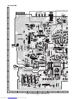
Page 14: ...R516 Q404 Q403 C423 R442 C420 C419 R427 R428 R429 C418 R431 R426 R425 D156 R171 D158 C508 L501 C509 C512 IC502 CNP103 C514 C186 C185 C505 R174 C506 R133 IC501 R134 R511 C513 R100 Q603 C136 C129 R124 R123 C120 R132 R112 R120 C138 C114 R110 C126 C118 C112 R136 R104 R116 C116 C124 R118 R114 R106 R108 R111 C108 C106 R122 C113 R102 C128 IC101 R101 R113 C105 C107 R117 R105 R107 C125 C115 R115 R131 R119 ...

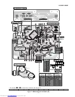
Page 15: ... R351 R352 C305 W102 AT CANCEL ROD ANTENNA SPRING 249 L301 LED260 LED258 LED256 LED254 LED401 LED1 IC1 L8 C123 C121 27 E H F G C B D A E C B C B A 1 2 3 3 2 1 1 2 3 2 3 4 5 1 7 8 9 6 TC2 TC1 TC4 TC3 VC2 VC4 VC3 VC1 BAND SELECTOR 2 3 4 5 1 7 8 9 6 F 1 1 5 10 12 13 15 20 24 L3 MW L4 SW1 L3 4 MW SW1 BAR ANTENNA ROD ANTENNA 253 BK WH FM MONO MIC HIGH NORMAL FM STEREO M501 TAPE MOTOR SW503 TAPE2 PLAY S...

Page 16: ... PWB A5 TERMINAL B PWB A6 POWER PWB A7 1 2 CNP601 CNS601 WH WH RD RD RD BK BL SW601 VOLTAGE SELECTOR AC220V 240V AC110V 127V OR OR BK SO601 AC SOCKET AC110V 127V AC220V 240V 50 60Hz T601 POWER TRANSFORMER 250 237 251 251 TO MAIN PWB P14 1 D F601 T4A L 250V BR COLOR TABLE RD R OR YL GR BL VL GY WH W BK PK BROWN RED ORANGE YELLOW GREEN BLUE VIOLET GRAY WHITE BLACK PINK BK ...

Page 17: ...1 5 10 12 13 15 20 24 1 1 8 2 3 1 2 3 1 2 3 4 5 1 6 2 3 4 5 1 6 7 1 7 WH WH WH WH WH WH BK 5 10 15 20 25 30 35 40 45 50 55 60 65 70 75 80 85 90 95 100 31 51 81 5 10 15 16 20 25 30 12 13 2 3 4 5 1 7 8 9 6 14 15 11 17 10 16 BR COLOR TABLE RD R OR YL GR BL VL GY WH W BK PK BROWN RED ORANGE YELLOW GREEN BLUE VIOLET GRAY WHITE BLACK PINK SW702 PICKUP IN M802 SPINDLE MOTOR M801 SLED MOTOR CNP803 5 4 7 6...

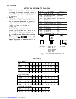
Page 18: ...ESCRIPTION POSITION SW1 BAND SELECTOR FM SW101 RECORD PLAYBACK PLAYBACK SW102 BEAT CANCEL A SW103 DUBBING SPEED MIC MIC FM MONO FM MODE SW401 SURROUND ON SW501 FUNCTION SELECTOR CD LINE SW601 VOLTAGE SELECTOR AC220 240V SW702 PICKUP IN OFF SW902 TAPE 2 MAIN OFF SW901 TAPE 1 MAIN OFF SW903 TAPE 2 PLAY OFF SW904 TAPE 2 DIRECTION A REF NO VOLTAGE Figure 18 TYPES OF TRANSISTOR AND LED 333ID213 VIEW FR...

Page 19: ...TOP PLAY TCD 782 TNO 02 PLAYBACK TEI 1 LO 1 TRO 2 RO 2 SBAD 3 1 2 3 4 6 7 11 15 16 17 5 6 5 7 8 5 9 10 6 11 12 13 14 6 11 15 6 11 15 IC802 66pin IC803 20pin IC802 45pin IC803 21pin IC802 72pin IC802 74pin IC802 62pin IC802 67pin IC802 64pin IC802 71pin IC802 62pin IC802 63pin IC802 67pin IC801 22pin IC802 71pin IC802 62pin IC801 19pin IC802 67pin IC801 17pin IC802 71pin IC802 64pin IC802 67pin IC8...

Page 20: ...nting product is prohibited by law Cleaning Disc PARTS CODE UDSKA0004AFZZ Cleaning Liquid When the CD does not function When the CD section does not operate when the objective lens of the optical pickup is dirty this section may not operate Clean the objective lens and check the playback operation When this section does not operate even after the above step is taken check the following items Remov...

Page 21: ...s Yes No No The optical pickup is faulty Check as stated in item FOCUS SERVO SAWTOOTH WAVE FAILURE Yes Check the periphery of IC801 and BI801 CNS801 Is it normal No Check the pattern between pin 13 of IC801 and pin 63 of IC802 Check the periphery of IC801 and BI801 CNS801 IC801 is faulty Yes Is 7 5V applied to the emiter of Q802 Is 5V applied to the collector of Q802 Yes No No Check the PWB patter...

Page 22: ...and IC803 No BI801 CNS801 connection failure or optical pickup failure Yes Spindle motor clv servo failure Is above wave obtained between pins 5 and 6 of IC803 Is following wave output to the pin 55 AVSS of IC802 when the Function is changed to PLAY from STOP No Yes Check the procedure in HF ERROR If OK IC802 is faulty Check the PWB pattern between pin 72 DMO of IC802 and pins 5 and 6 of IC803 If ...

Page 23: ...Is the following wave output to the pins 12 TEO of IC801 during track search in normal playback Yes Yes No Check as stated in item SLED MOTOR OPERATION FAILURE No IC802 failure No Check the PWB pattern between pin 67 TRO of IC802 and pin 28 of IC803 Check the PWB pattern between pins 25 and 26 of IC803 and Optical pickup If OK Optical pickup failure Yes Is the above wave output to the pins 64 TEI ...

Page 24: ...STP instruction executed the device s current consumption is reduced to 1µA or less allowing for the supply voltage to be lowered to 2 0V The device is reset and the program starts from address 0 when a voltage of 2 7V or more is applied to this pin when it is at 0V power on reset 21 K0 P1 0 TRAY CLOSE Input 4 bit CMOS I O ports 22 K1 P1 1 TRAY OPEN Input These ports can be set for input or output...

Page 25: ...y a program 43 DOUT DOUT Input Output Digital output pin 44 SBSY SBSY Input Output Subcode block sync output pin It outputs a high at the S1 position when subcode sync is detected 45 SBOK SBOK Input Output Subcode Q data CRCC determination result output pin It outputs a high when CRCC check is found OK 46 VDD VDD1 Input Output CD unit s digital block power supply pins 47 VSS VSS1 Input Output Norm...

Page 26: ...ged for output ports if they have been set for CD control signal input output pins 77 XVSS XVSS Input Output CD s crystal oscillator power supply pins Normally connect these pins to the power supply lines that are used in common for the VDD and VSS pins 78 XI XI Input Output CD s crystal oscillator input output pins 79 XO XO Input Output Normally connect 16 934MHz here This clock is used as the sy...

Page 27: ... pulses or generate an interrupt at a given pulse count address 3 93 MXO MXO Crystal oscillator pins for the controller 94 MXI MXI The oscillator clock is used as the timebase for the clock facility or as the controller s system clock Connect a 4 5MHz or 75kHz crystal resonator to the MXO and MXI pins Since these pins do not contain internal feedback resistors etc an amp resistor or output resisto...

Page 28: ... 28 GX CD1200W M E M O ...

Page 29: ... type without lead wire VC MN Cylindrical type without lead wire VC TV Square type without lead wire VC TQ Square type without lead wire VC CY Square type without lead wire VC CZ Square type without lead wire VC J The 13th character represents capacity difference J 5 K 10 M 20 N 30 C 0 25 pF D 0 5 pF Z 80 20 If there are no indications for the electrolytic capacitors error is 20 Resistors VRD Carb...

Page 30: ...01BGZZ J AC 100 kohm B 2 Graphic Equalizer VR401 RVR B0002BGZZ J 50 kohms B 2 VOLUME VARIABLE CAPACITORS TC5 6 RTO H1003SJZZ J AG Trimmer 5 pF TC7 8 RTO H1001BGZZ J AD Trimmer 10 pF TC9 RVC Z0001BGZZ J AF Fine Tuning VC1 4 RVC R0001BGZZ J AK Variable Capacitance with Trimmer TC1 4 VIBRATOR XL801 RCRM 0008AWZZ J AF Ceramic 16 93 MHz CAPACITORS C2 VCCCPU1HH5R0J J AA 5 pF CH 50V C4 VCCCPU1HH240J J AA...

Page 31: ...0V Mylar C832 RC GZA476AF1A J AB 47 µF 10V Electrolytic C833 VCQYKA1HM333K J AB 0 033 µF 50V Mylar C834 835 VCKYPA1HB471K J AA 470 pF 50V C836 839 VCQYKA1HM473K J AB 0 047 µF 50V Mylar C840 842 VCKZPA1HF473K J AA 0 047 µF 50V C843 RC GZA476AF1A J AB 47 µF 10V Electrolytic C844 RC GZA107AF1A J AB 100 µF 10V Electrolytic C845 VCKZPA1HF473Z J AA 0 047 µF 50V C846 RC GZA225AF1H J AB 2 2 µF 50V Electro...

Page 32: ...1BGZZ J Connector Ass y 6 6Pin CNP101 QCNCM705CAFZZ J AA Plug 3Pin CNP102 QCNCM705DAFZZ J AB Plug 4Pin CNP103 QCNCM698JAFZZ J AC Plug 9Pin CNP501 QTANA0001BGZZ J AD Terminal Speaker CNP601 QCNCM035BAWZZ J AB Plug 2Pin CNP803 92LCONE6P53254 J AC Plug 6Pin CNP804 QCNCM705FAFZZ J AB Plug 6Pin CNS101 QCNWN0001BGZZ J AD Connector Ass y 3Pin CNS102 QCNWN0002BGZZ J AE Connector Ass y 4Pin CNS103 QCNWN000...

Page 33: ...partment Lid GL 264 TSPC 0017BGZZ J Label Specifications GL For Malaysia Asia Middle East Africa 264 TSPC 0018BGZZ J Label Specifications GL For Jordan Egypt 264 TSPC 0020BGZZ J Label Specifications GL For Thailand 264 TSPC 0026BGZZ J Label Specifications BK For Malaysia Asia Middle East Africa 264 TSPC 0027BGZZ J Label Specifications BK For Jordan Egypt 264 TSPC 0028BGZZ J Label Specifications BK...

Page 34: ...GANE0003BGZZ J Warranty Card For Australia TINSZ0008BGZZ J Operation Manual TLABB0001BGZZ J AB Label Japan TLABB0002BGZZ J AC Label Japan TLABE0005BGZZ J Label Ean Bar Code GL TLABE0008BGZZ J Label Ean Bar Code BK TLABR1137BGZZ J Label Bar Code GL TLABR1138BGZZ J Label Bar Code BK TLABS0002BGZZ J Label Laser TLABS0003BGZZ J Label Class 3 TLABZ0001BGZZ J Label Contru origin for Set TLABZ0002BGZZ J ...

Page 35: ...GX CD1200W A B C D E F G H 1 2 3 4 5 6 Figure 6 CD MECHANISM EXPLODED VIEW 6 701 304 701 302 301 702 303 M802 703x2 305x2 SW702 M801 305 PWB B 704 306 307 ...

Page 36: ... 257 260 PWB A3 601x2 PWB A1 601x2 601x2 601 605x5 214x2 201 601 213 601 262 261 238 244 604 602x2 TAPE MECHANISM 605x6 300 300 1 300 2 300 3 300 4 300 5 300 6 300 7 300 8 300 9 300 10 M501 300 11 SW902 300 12 SW901 300 13 SW903 300 14 SW904 222 223 224 225 226 227 228 230 229 231 232 233 203 215 209 208 202 242 601 206 221 212 216 210 205 204 601x3 PWB C3 PWB A4 PWB A2 215 602x2 251 251 Q601 IC40...

Page 37: ...EW BLACK BLACK RED RED WOOFER SP401 L CH SP402 R CH TWEETER SP403 L CH SP404 R CH TWEETER SP403 L CH SP404 R CH WOOFER SP401 L CH SP402 R CH 701x4 305 702x5 301 LEFT 302 RIGHT 303 LEFT 304 RIGHT SP403 L CH SP404 R CH SP401 L CH SP402 R CH 305 305 306 307 305 308 309 8 ...

Page 38: ...GX CD1200W M E M O 9 ...

Page 39: ...GX CD1200W M E M O 10 ...

Page 40: ...iroshima Hiroshima 739 0192 Japan Printed in Japan COPYRIGHT 2000 BY SHARP CORPORATION ALL RIGHTS RESERVED No part of this publication may be reproduced stored in a retrieval system or transmitted in any from or by any means electronic mechanical photocopying recording or otherwise without prior written permission of the publisher ...

Reviews: