6 – 16
GX10i
CONFIDENTIAL
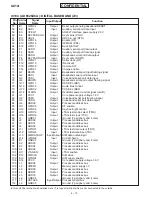
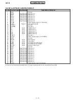
IC901 VHIHD155148-1L (HD155148TF): RF
Pin No. Terminal name Input/Output
Description of terminal
1
GNDLNA
–
Ground for LNA bias
2
VCCLNA
Input
VCC for LNA transistor and LNA bias
3
GNDDUM,GNDPCS
–
Ground for emitter of LNA transistor (PCS)
4
PCSLNAI
Input
Positive input for LNA transistor (PCS)
5
PCSLNAIB
Input
Negative input for LNA transistor (PCS)
6
GNDPCSB,GNDDCS
–
Ground for emitter of LNA transistor (PCS,DCS)
7
DCSLNAI
Input
Positive input for LNA transistor (DCS)
8
DCSLNAIB
Input
Negative input for LNA transistor (DCS)
9
GNDDCSB,GNDGSM
–
Ground for emitter of LNA transistor (DCS,GSM)
10
GSMLNAI
Input
Positive input for LNA transistor (GSM)
11
GSMLNAIB
Input
Negative input for LNA transistor (GSM)
12
GNDGSMB,GNDDUM
–
Ground for emitter of LNA transistor (GSM)
13
VCCLNA
Input
VCC for LNA transistor and LNA bias
14
GNDOPLL
–
Ground for OPLL
15
VCOIN
Input
TXVCO signal input
16
VCCOPLL
Input
VCC for OPLL and phase comparator
17
PLLOUT
Output
Current output to control and modulate TXVCO
18
VCCIQ/ADDAC
Input
VCC for IQ modulator and offset canceling AD/DAC
19
GNDIQ/ADDAC
–
Ground for IQ modulator and offset canceling AD/DAC
20
IINB
Input
Negative input of I signal for modulator
21
IIN
Input
Positive input of I signal for modulator
22
QINB
Input
Negative input of Q signal for modulator
23
QIN
Input
Positive input of Q signal for modulator
24
QOUTB
Output
Negative output of Q channel
25
QOUT
Output
Positive output of Q channel
26
IOUTB
Output
Negative output of I channel
27
IOUT
Output
Positive output of I channel
28
VCCIFVCO
Input
VCC for IFVCO and IFVCO buffer and divider
29
GNDIFVCO
–
Ground for IFVCO buffer an divider
30
VCCOSC
Input
VCC for IFVCO
31
TCXOCONT
–
TCXOOUT frequency (GND: 26 MHz/VCC: 13 MHz)
32
VCCIFSYN
Input
VCC for IF synthesizer and TCXOOUT buffer (13 MHz/26 MHz)
33
CPIFSYN
Output
Charge pump output of IF synthesizer
34
GNDIFSYN
–
Ground for IFsynthesizer and TCXOOUT buffer (13 MHz/26 MHz)
35
LE
Input
Load enable for serial data
36
TCXOOUT
Output
TCXO output for base band
37
CLK
Input
Clock for serial data
38
TCXOIN
Input
TCXO input for IF and RF synthesizer
39
SDATA
Input
Serial data
40
GNDRFSYN
–
Ground for RF synthesizer and TCXO input buffer (26 MHz)
41
VCCRFSYN
Input
VCC for RF synthesizer and TCXO input buffer (26 MHz)
42
BANDSW
Output
Band select or frequency select switch for RFVCO
43
FLOCK
Output
Fast lock control for RF synthesizer
44
CPRFSYN
Output
Charge pump output of RF synthesizer
45
GNDBB
–
Ground for base band
46
VCCBB
Input
VCC for base band
47
VCCRFLO
Input
VCC for RF local buffer and divider
48
GNDRFLO
–
Ground for RF local buffer and divider
49
RFLOINB
Input
Negative input for RF local
50
RFLOINB
Input
Positive input for RF local
51
GNDMIX
–
Ground for direct conversion mixer
52
CAPQB
Output
Capacitor for Q channel LPF (Negative output)
53
CAPQ
Output
Capacitor for Q channel LPF (Positive output)
54
CAPIB
Output
Capacitor for I channel LPF (Negative output)
55
CAPI
Output
Capacitor for I channel LPF (Positive output)
56
VCCMIX
Input
VCC for direct conversion mixer


