5 – 1
GX10i
CONFIDENTIAL
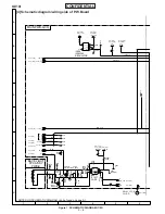
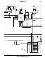
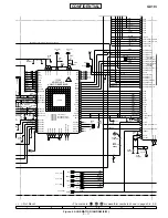
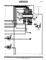
CHAPTER 5. SCHEMATIC DIAGRAM AND WIRING SIDE OF P.W.BOARD
TOP VIEW
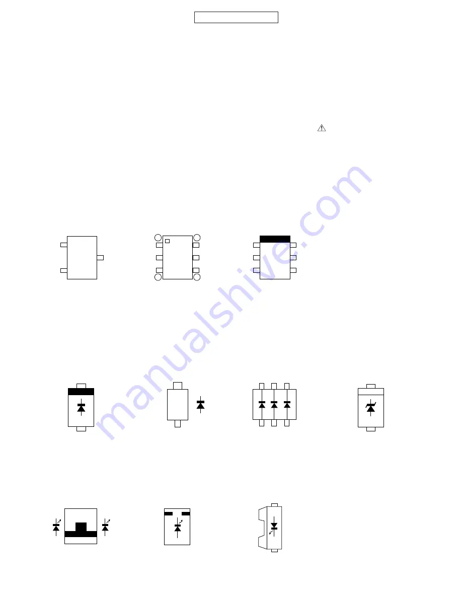
1SS388
RB160M30
RB520S30
RB521S30
B
(3)
(G)
1
(S)
2
(D)
3
(G)
6
(G)
5
(D)
4
(S)
C
(2)
(D)
E
(1)
(S)
2SA1955 A
2SA1989 SR
2SK3019
3LP02 M
MCH3443
RT1N144 U
RT1N234 U
TOP
VIEW
CW215TBS
TOP VIEW
CPH6311
EMD6
EMD9
EMD12
EMG9
MCH6613
UM6K1
D
D
G
D
D
S
TOP
VIEW
1
3
6
4
TOP
VIEW
BOTTOM VIEW
CL165UR
TOP VIEW
MA2ZD02
HN2S01FU
TOP VIEW
TOP VIEW
YPY1105C
TOP VIEW
RD22SL
RSB6.8S
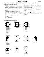
[2] Types of transistor and LED
[1] Notes on schematic diagram
• Resistor:
To differentiate the units of resistors, the symbols K and M
are used. The symbol K means 1000 ohm and the symbol
M means 1000 kohm. The resistor without any symbol is an
ohm resistor.
• Capacitor:
To indicate the unit of capacitor, the symbol is used.
The symbol P means pico-farad and the unit of the capacitor
without such a symbol is microfarad. As to electrolytic
capacitor, the expression “capacitance/withstand voltage”
is used.
(CH), (RH), (UJ): Temperature compensation
(ML): Mylar type
(S): Styrol type
(PP): Polypropylene type
• The indicated voltage in each section is the one measured
by Digital Multimeter between such a section and the
chassis with no signal given.
• Schematic diagram and Wiring Side of P.W. Board for this
model are subject to change for improvement without prior
notice.
• Parts marked with “
” are important for maintaining the
safety of the set. Be sure to replace these parts with
specified ones for maintaining the safety and performance
of the set.

