background image

XL-HP535H/HP535E

3 – 1

Audio

XL-HP535H/HP535E

Service Manual

XLHP535H

Market

E


CHAPTER 3. 

MECHANICAL DESCRIPTION

[1] REMOVING AND REINSTALLING THE
MAIN PARTS

1. TAPE MECHANISM SECTION

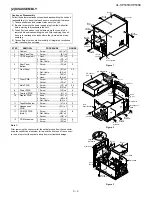
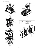
Perform steps 1 to 9 of the disassembly method to remove the tape
mechanism.(see page 3-3,3-4)

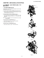
1.1. How to remove the Record/Playback Head (See Fig. 1)

1. When you remove the screws (A1) x 2 pcs and (A2) x 1 pc., the

record/playback head can be removed.

1.2. How to remove the Pinch Roller (See Fig. 2)

1. Carefully bend the pinch roller pawl in the direction of the arrow

<

A

>, and remove the pinch roller (B1) x 1 pc., in the direction of the

arrow <

B

>.

NOTE: When installing the pinch roller, pay attention to the spring

mounting position.

1.3. How to remove the Belt (See Fig. 3)

1. Remove the main belt (C1) x 1 pc., from the motor side.

2. Remove the FF/REW belt (C2) x 1 pc.

1.4. How to remove the Motor (See Fig. 4)

1. Remove the screws (D1) x 2 pcs., to remove the motor.

Figure 1

Figure 2

Figure 3

Figure 4

(A1)x2
Ø2x6mm

(A2)x1
Ø2x9mm

Record/Playback
Head

Erase Head

Clutch Ass'y

Pinch Roller

(B1)x1

<A>

<B>

Pinch

Roller

Pawl

Pull

Main Belt

(C1)x1

FF/REW

Belt

(C2)x1

Motor

FF/REW

Clutch

Flywheel

(D1)x2

Ø

2.6x5mm

Motor

Clutch Ass'y

Summary of Contents for Illustration XL-HP535E

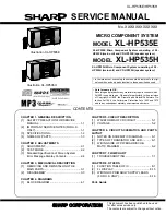
Page 1: ...YPES OF TRANSISTOR AND LED 6 1 3 WIRING SIDE OF P W BOARD SCHE MATIC DIAGRAM 6 2 CHAPTER 7 FLOWCHART 1 TROUBLESHOOTING 7 1 CHAPTER 8 OTHERS 1 FUNCTION TABLE OF IC 8 1 2 FL DISPLAY 8 15 3 WIRING OF PRIMARILY SUPPLY LEADS FOR U K ONLY 8 16 Parts Guide XL HP535E Micro Component System consisting of XL HP535E main unit and CP HP535E speaker system XL HP535H MODEL XL HP535H Micro Component System consi...

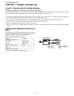
Page 2: ...have already been adjusted prior to shipping 3 No adjustment to the Laser Power should be attempted when replacing or servicing the Pickup 4 Under no circumstances look directly into the Pickup Lens at any time 5 CAUTION Use of controls or adjustments or performance of procedures other than those specified herein may result in hazardous radiation exposure 2 IMPORTANT SERVICE NOTES FOR U K ONLY Bef...

Page 3: ...bs each XL HP535H General Amplifier CD player Tuner Cassette deck Speaker Power source AC 230 V 50 Hz Power consumption Power on 90 W Power stand by 0 6 W Dimensions Width 185 mm 7 1 4 Height 260 mm 10 1 4 Depth 307 mm 12 Weight 6 1 kg 13 4 lbs This power consumption value is obtained when the demonstra tion mode is cancelled in the power stand by mode Refer to page 9 to cancel the demonstration m...

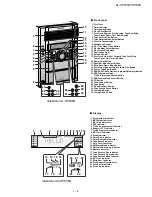
Page 4: ...Pause Button 26 Tuning Up Button 27 Tuning Down Button 1 11 12 14 15 16 17 18 19 20 10 2 3 4 13 9 5 6 7 8 23 24 21 26 27 25 22 Display 1 Disc Number Indicators 2 MP3 Folder Indicator 3 MP3 Title Indicators 4 MP3 Total Indicator 5 Sleep Indicator 6 Timer Play Indicator 7 Timer Recording Indicator 8 Tape Record Indicator 9 Daily Timer Indicator 10 FM Stereo Mode Indicator 11 FM Stereo Receiving Indi...

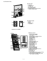
Page 5: ...rch Button 23 RDS Display Mode Select Button 24 CD Button 25 Tuner Band Button 26 Tape Button 27 Video Auxiliary Button 28 Tape Record Pause Button 29 Tuning Up Button 30 Tuning Down Button 1 11 12 15 16 17 18 19 20 10 2 3 4 9 5 6 7 8 26 27 29 30 28 21 22 24 25 23 14 13 Illustration XL HP535H Display 1 Disc Number Indicators 2 MP3 Folder Indicator 3 MP3 Title Indicators 4 RDS Indicator 5 Traffic A...

Page 6: ...utton 8 CD Button 9 Tuner Band Button 10 Tape Button 11 Video Auxiliary Button 12 Volume Up and Down Buttons 13 Disc Random Button 14 Disc Clear Dimmer Button 15 Disc Stop Button 16 Tape Reverse Play Button 17 Tape Stop Button 18 Memory Set Button 19 Disc Pause Button 20 Disc Play or Repeat Button 21 Tape Forward Play Button 22 Tape Record Pause Button 23 MP3 Disc Navigation Mode Select Button 24 ...

Page 7: ...IC so that the loop gain at the gain crossover frequency will be 0 dB Focus gain adjustment Tracking gain adjustment 4 CD ERROR CODE DESCRIPTION CHECKING If Error is detected CHECKING will be displayed instead of ER CD ER CD display will only be displayed when error had been detected for the 5th times Torque Meter Specified Value Play TW 2111 Over 80 g Torque Meter Specified Value Play TW 2111 30 ...

Page 8: ... E S T A Do TOC IL Do normal play When these following key is input into PLAY key track num ber can be appoint directly MEMORY key input 1 key Track 4 2 key Track 9 3 key Track 15 Adjustment result automatically will display as below for each 2 sec a FOF_XXXX b TOF_XXXX c TBAL_XX d TGAN_XX f FGAN_XX g RFLS_XX STOP key input STOP explanation a Focus off set FOF_XXXX b Tracking off set TOF_XXXX c Tr...

Page 9: ...t specific point MEMORY key input Adjustment result automatically will display as below for each 2 sec a FOF_XXXX b TOF_XXXX c TBAL_XX d TGAN_XX f FGAN_XX g RFLS_XX STOP key input STOP explanation a Focus off set FOF_XXXX b Tracking off set TOF_XXXX c Tracking balance TBAL_XX d Tracking Gain TGAN_XX f Focus Gain FGAN_XX g RF level shift RFLS_XX VOL Last memory P GEQ FLAT X BASS OFF To cancel Power...

Page 10: ... condition when irregular process occur on power supply line BEFORE TRANSPORTING THE UNIT The following process need to be taken after set tapering parts replacement 1 Press the ON STAND BY button to enter stand by mode 2 While pressing down the button and the X BASS DEMO button press the ON STAND BY button The Micro Computer version number will be displayed as UM upper case 3 Press OPEN CLOSE but...

Page 11: ...bend the pinch roller pawl in the direction of the arrow A and remove the pinch roller B1 x 1 pc in the direction of the arrow B NOTE When installing the pinch roller pay attention to the spring mounting position 1 3 How to remove the Belt See Fig 3 1 Remove the main belt C1 x 1 pc from the motor side 2 Remove the FF REW belt C2 x 1 pc 1 4 How to remove the Motor See Fig 4 1 Remove the screws D1 x...

Page 12: ...echanism is at tray No 1 play position and to remove CD located in tray No 3 the procedure is as follows If the gear up down board is located at tray No 1 position then rotate Reduction gear C clock wise until Disc tray is at STOCK position Rotate reduction gear D clock wise Figure 3 to move the CD mechanism to tray No 3 position This is confirmed by check ing the gear up down board position Base ...

Page 13: ... A1 x11 1 2 Rear Panel Top 1 Screw B1 x2 1 3 CD Changer unit 1 Hook C1 x2 2 Socket C2 x1 3 Flat Cable C3 x1 2 4 Rear Panel Bottom 1 Screw D1 x8 2 5 Front Panel 1 Screw E1 x3 2 Flat Cable E2 x2 3 Socket E3 x1 4 Hook E4 x2 2 3 3 6 Tuner PWB 1 Screw F1 x1 2 Socket F2 x1 2 3 7 Main PWB 1 Screw G1 x2 2 Socket G2 x4 2 4 4 8 Power PWB 1 Screw H1 x4 4 9 Terminal PWB 1 Screw J1 x1 4 10 Display PWB 1 Knob K...

Page 14: ...PWB Tape Mechanism N1 x2 ø3x10mm N2 x2 N3 x1 P1 x2 ø3x10mm P1 x2 ø3x10mm CD Changer Unit CD MP3 PWB Figure 7 STEP REMOVAL PROCEDURE FIGURE 1 Woofer Tweeter 1 Net Frame A1 x1 2 Catching Holder A2 x4 3 Screw A3 x4 4 Front Panel A4 x1 5 Screw A5 x6 8 Figure 8 P2 x4 ø2 6x10mm CD Changer Unit CD Mechanism Net Frame A1 x1 Screwdriver A5 x2 ø3 5x14mm A3 x2 ø3 5x16mm A2 x2 A2 x2 A3 x2 ø3 5x16mm A5 x4 ø3 5...

Page 15: ...XL HP535H HP535E 3 5 MEMO ...

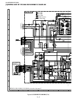
Page 16: ... N P B REC A_ 10V LD_ 8V F OUT ST FM R L IF OUT AM IN FM IN COVERAGE AM BAND TRACKING AM TERMINAL ANTENNA 5 1V FM IF L341 BALUN ANTENNA AM LOOP FM B B5 CL AM IF 456kHz 10 7MHz 450kHz DO DI CE MO ST SWITCHING FM AM PLL TUNER LC72131 FM AM OUT R L FM AM MPXIN STEREO AM RF IN AM OSC IN VSM FM VT OSC 4 5MHZ MO ST VCO FM DET FM B GND AM IF FM IF DET LA1832S AM MIX OUT FM FRONT END AM OSC OUT FM MPX AM ...

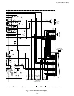
Page 17: ...T B10 B10 LED701 LED708 B5 VDD B3 FAN MOTOR FL DISPLAY CE CLK DI DO TO CD SECTION RESET AVDD REMOCON HEADPHONES SUB WOOFER PRE OUT SPEAKER TERMINAL M SYSTEM MUTE 8 11 6 1 14 18 7 48 5 2 44 43 24 21 15 12 11 7 6 10 17 18 19 20 3 4 2 1 50 51 2 3 1 31 30 29 47 53 56 41 42 45 79 36 38 46 25 40 13 33 34 39 1 2 16 SUB MAIN MOTOR DRIVER SOLENOID A_ 10V LD_ 8V SW701 SW705 SW706 SW708 H Only SW709 SW728 S3...

Page 18: ...SC PHOTO 5V CAM CAM TR TR CNP6 CNP5 16 9344MHz 3 3V 3 3V Q2 DRIVER LASER PICKUP UNIT FOCUS COIL TRACKING COIL PICKUP IN SW1A LC78648E IC1 XL1 CD DIGITAL SIGNAL PROCESSOR 24 23 22 21 75 74 70 36 35 PU IN CONT1 34 20 19 32 61 79 48 45 44 42 41 47 66 65 64 68 67 63 62 51 53 59 69 15 16 1 6 11 14 13 12 5 10 3 7 9 8 4 2 27 1 26 60 80 XVDD 49 7 8 9 10 14 15 28 40 25 CNP2 8V 5V DGND L CH AGND R CH D_GND ...

Page 19: ...06AW SYS CE SYS CL SYS DO AVDD VDD VDD FOCUS TRACKING 4 19MHz D RAM 28 33 34 21 24 31 32 4 3 1 35 13 11 15 17 2 36 6 5 27 9 10 19 23 22 20 25 19 18 11 10 30 12 14 29 17 43 15 16 1 44 28 26 27 9 23 24 37 2 1 3 27 28 29 21 35 1 6 20 53 50 30 33 40 23 42 60 41 2 5 7 10 39 40 34 36 31 26 22 19 16 14 13 76 75 32 69 62 14 20 22 52 10 12 8 6 43 44 45 68 61 51 31 21 11 77 73 66 80 9 79 7 5 4 3 2 1 MO_B MO...

Page 20: ...ilter Offset 3 IC1 68 4 IC1 17 T T FDO SPDO Stopped CH1 200 mV DC 10 1 CH2 500 mV DC 10 1 500 ms div 1999 04 07 09 51 15 500 ms div NORM 20 kS s 2 1 Record Length Smoothing ON CH1 0 000 V CH2 0 000 V Main 100 K Zoom 2 K Mode NORMAL Type EDGE CH2 Delay 2 924 ms Hold off 0 2 µs CH3 0 00 V CH4 0 00 V BW FULL Trigger Filter Offset 1 IC1 21 6 IC1 24 T FDO PDO2 PDO1 Stopped CH1 500 mV DC 10 1 CH3 1 V DC...

Page 21: ...0 V 0 36 V 0 00 V 4 94 V 4 78 V 4 81 V 4 81 V 4 92 V 4 80 V 4 80 V 4 80 V 4 80 V 4 80 V 4 79 V 4 80 V 4 80 V 4 92 V 4 80 V 4 80 V 4 77 V 4 94 V 4 92 V 9 88 V 0 00 V 1 2 3 4 5 6 7 8 9 10 11 12 13 14 15 16 17 18 19 20 21 22 23 24 PIN NO VOLTAGE IC601 2 52 V 0 00 V 0 40 V 0 00 V 0 00 V 5 05 V 9 86 V 4 70 V 0 00 V 0 00 V 5 14 V 0 00 V 5 14 V 0 00 V 0 00 V 2 54 V 5 16 V 0 00 V 0 00 V 9 87 V 0 00 V 2 52...

Page 22: ...XL HP535H HP535E 5 3 MEMO ...

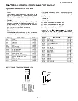
Page 23: ...layed back 4 In the power section a tape is being played back 5 In the CD section the CD is stopped Parts marked with are important for maintaining the safety of the set Be sure to replace these parts with specified ones for maintaining the safety and performance of the set 2 TYPES OF TRANSISTOR AND LED REF NO DESCRIPTION POSITION SW1 CLAMP ON OFF SW1A PICKUP IN ON OFF SW2 TRAY SW1 ON OFF SW3 TRAY...

Page 24: ...P 3 3K KTC3200 GR KTC3200 GR 47K 4 7K KTC3875 GR 0 0015 15K 12K 6 8K 47 25 330P 1K 100 16 56 560P 0 033 100K 3 9K 12K 56 330P 1K 100 16 560P 47 25 6 8K 0 033 100K 3 9K 1 5K 270P 4 7K 68K 100 22 16 0 022 220 10 10K 22 16 0 0033 47 25 5 6K 0 022 LC75341 AUDIO PROCESSOR AN7345K PLAYBACK AND RECORD 220P 220P 1K 1K 3 3 50 0 022 22 16 5 6K 4 7K 270P 1 5K 100 0 022 10K 47 25 0 0033 180P CH KTC3200 GR 3 3...

Page 25: ... FROM TUNER PWB XL HP535E 6 9 9 G XL HP535H 6 11 9 G K R K K Nor CrO2 RIPPLE ALC ALC VCC R1 R2 R3 R4 RSEL0 RIN RTRE RBASS ROUT VREF VDD CLK CHASSIS GND 1 2 3 FFC701 CNP701A H ONLY CNS303 RDS READY RDS RDCL RDS RDDA RDS RST TUN_SM SPAN 27 26 25 24 23 22 27 RDS_READY RDS_RDCL RDS_RDDA RDS_RST TUN_SM 22 16 0 022 220 10 10K 47 25 330µH 220 47K 4 7K 82 4 7 0 039 ML 0 0082 22K 47K KTC3203 Y 47 25 KTA150...

Page 26: ...0 1 8K 1 5K 0 01 0 22 10 10 0 1 47K 47K 3300 63 1N4004S DZ12BSB 33K 47 50 56K 56K 0 1 39K 39K DS1SS133 1N4004S KTC3875 GR 4700 35 DS1SS133 KTC3875 GR 100 56K 3P CH CH CH CH 1K 56K 3300 63 4700 35 DZ12BSB 100 100 1 5K 1 5K 22 50 560 100P 560 1 5K 0 001 0 001 56K 100 100 1K 22 50 56K 0 01 KTC3875 GR 3µH 3µH 0 1 1 8K 0 22 1K 100 100 1K 56K 0 22 100P 3P 100 100 100 STK412 490 3W 3W ML 1 2W 1 2W 1 4W 1...

Page 27: ...3 POWER PWB A2 POWER TRANSFORMER MAIN TF T1 6A L 250V GND VL VL VH VH D3SBA60F RL204F 0 22 0 22 D10XB60F 0 1 0 1 T3 15A L 250V ML ML DZ6 8BSA 100 35 47K 0 1 RL204F 0 1 T2A L 250V T2A L 250V ML ML 10 DZ6 2BSA 12K 1 4 1 4 KTA1274 Y 100K 220 63 2 2K 47 50 DZ30BSB 1N4004S 1N4004S 22 100 1 4W 1 2W 47 47 47K 47 50 0 022 DS1SS133 AN78L05 VOLTAGE REGULATOR 3 1 2 1 2 3 4 5 6 7 8 9 10 1 3 2 AC 230 240V 50Hz...

Page 28: ...0 50 1 8K 1 5K 0 01 10 0 1 47K 47K 3300 63 1N4004S DZ12BSB 33K 47 50 56K 56K 0 1 39K 39K DS1SS133 1N4004S KTC3875 GR 4700 35 DS1SS133 KTC3875 GR 100 56K 3P CH CH CH CH 1K 56K 3300 63 4700 35 DZ12BSB 100 100 1 5K 1 5K 22 50 560 100P 560 1 5K 0 001 0 001 56K 100 100 1K 22 50 56K 0 01 KTC3875 GR 3µH 3µH 0 1 1 8K 0 22 1K 100 100 1K 56K 0 22 100P 3P 100 100 100 STK412 490 3W 3W ML 1 2W 1 2W 1 4W 1 4W 1...

Page 29: ...0V ML ML DZ6 8BSA 100 35 47K 0 1 RL204F 0 1 T2A L 250V T2A L 250V ML ML 10 DZ6 2BSA 1000 6 3 12K 1 4 1 4 KTA1274 Y 100K 220 63 2 2K 47 50 DZ30BSB 1N4004S 1N4004S 22 100 1 4W 1 2W 47 47 47K 47 50 82 1N4004S 220 0 022 DS1SS133 1K 47K KTC3199 GR 1 4W 1N4004S 1N4004S 1N4004S 1N4004S 0 047 ML 470 35 AN78L05 VOLTAGE REGULATOR 3 1 2 1 2 3 4 5 6 7 8 9 10 1 3 2 AC 230V 50Hz AC POWER SUPPLY CODE 228 LINE FI...

Page 30: ...3 0 022 0 022 0 022 470 100 16 15 2 2µH 0 022 4 7K 0 0 001 2SC380 0 33 680 6 8K 330 33 0 01 15P 0 01 10 50 2 2K 1 50 1 5K 12P 150 1K 1K 1K 0 001 47 16 0 022 10K 1K 4 5MHZ 0 022 0 001 100µH 2 B B B B 1K 330P 47K LC72131 0 022 0 022 0 022 10 16 1K 0 022 0 022 1K 5 6K 560P 22P 68K SVC347S 10K 15P 0 047 0 022 10K 0 022 2 2 50 3 9K 0 022 1 50 2 7K 0 022 2 2 50 0 001 0 022 LOW PA FILTER PLL TUNER C323 D...

Page 31: ... TUNER PWB C CNP303 100P 0 01 0 001 00µH 22K B B B B 1K 4 7K 47K 330P 47K 0 022 1K 270 0 022 0 022 3 9K 2 2 50 1 50 3 3K 1 50 1K 100 10 0 001 22P CH 10 7MHZ 5 6K LA1832S 1 50 2 7K 456KHZ 1 50 1 50 470K 1K 1 50 27P CH 0 015 0 015 5 6K 220 DZ5 1BSB 100 10 0 022 220 100µH KTA1504 GR 5 6K 47 16 5 6K 1 8K 0 001 LOW PASS FILTER C383 C385 C388 L351 R386 R376 R360 CNS303 R395 C386 R377 CF352 C399 R352 R35...

Page 32: ...022 0 022 0 022 470 100 16 15 2 2µH 0 022 4 7K 0 0 001 2SC380 0 33 680 6 8K 330 33 0 01 15P 0 01 10 50 2 2K 1 50 1 5K 12P 150 1K 1K 1K 0 001 47 16 0 022 10K 1K 4 5MHZ 0 022 0 001 100µH 2 B B B B 1K 330P 47K LC72131 0 022 0 022 0 022 10 16 1K 0 022 0 022 1K 10 7MHZ 5 6K 560P 22P 68K SVC347S 10K 15P 0 047 0 022 10K 0 022 2 2 50 3 9K 0 022 1 50 2 7K 0 022 2 2 50 0 001 0 022 LOW PAS FILTER PLL TUNER C...

Page 33: ...1K 4 7K 47K 330P 47K 0 022 1K 270 0 022 0 022 3 9K 2 2 50 1 50 3 3K 1 50 1K 100 10 0 001 22P CH 10 7MHZ 5 6K LA1832S 1 50 2 7K 456KHZ 1 50 1 50 470K 1K 1 50 27P CH 0 015 0 015 6 8K 10K 0 022 22P CH 47 10 4 332MHZ 1K 1K 1K 10K 2 2µH 2 2µH 1K 0 022 10 16 47 10 0 022 560P 0 022 56K 56K 10K 0 022 KTC3875 GR 22P CH LC72723 RDS DECORDER 1K 5 6K 220 DZ5 1BSB 100 10 0 022 220 100µH KTA1504 GR 5 6K 47 16 5...

Page 34: ...ROTECT S8 S9 KEY 2 KEY 1 KEY 0 S15 S16 DIST 3 CLK B B B B B B B B M_ 13V CD_DRF DISC SW AC_RLY TRAY SW2 S18 DIST 1 S14 S10 S13 S12 S11 S9 S15 S14 S10 DIST FPA FPB SW KEY 1 G9 F1 1 45 46 47 50 51 44 43 42 41 40 39 38 37 36 35 34 33 32 31 30 29 28 27 26 25 24 23 22 21 20 19 18 17 16 15 14 13 12 11 10 9 8 5 4 2 1 1 2 3 1 2 2 KEY GND DISC 5 DISC 4 DISC 3 OPEN DISC 1 DISC 2 PLAY DIRECT CLOSE SWITCH PWB...

Page 35: ... B B B B B B B B B B B B B B B B B B B B SW_5V M_ 13V UN_SW5 6V S_MUTE AUX TIMER CLOCK TIME UP UP DOWN DOWN STOP PLAY TUNING TUNING TIME MEMORY SET DEMO MODE REVERSE REVERSE PLAY TRAY SW1 PRESET PRESET STANDBY REC F1 21 8 7 9 11 10 14 15 16 16 13 12 9 8 5 4 2 1 9 8 7 5 17 18 3 15 4 6 13 11 14 21 12 2 1 1 19 20 10 16 6 2 3 1 4 5 6 2 3 1 1 4 5 6 17 11 B CNP5 TO CD MP3 PWB 6 3 12 F CNP701B TO MAIN PW...

Page 36: ... F2 F2 P06 CLAMP SW T_SOL PROTECT S8 S9 KEY 2 KEY 1 KEY 0 S15 S16 DIST 3 CLK B B B B B B B B M_ 13V CD_DRF DISC SW AC_RLY TRAY SW2 S18 DIST 1 S14 S10 S13 S12 S11 S9 S15 S14 S10 DIST FPA FPB SW KEY 1 G9 F1 1 45 46 47 50 51 44 43 42 41 40 39 38 37 36 35 34 33 32 31 30 29 28 27 26 25 24 23 22 21 20 19 18 17 16 15 14 13 12 11 10 9 8 5 4 2 1 1 2 3 1 2 2 KEY GND DISC 5 DISC 4 DISC 3 OPEN DISC 1 DISC 2 P...

Page 37: ... B B B B B B B B B B B B B B B SW_5V M_ 13V UN_SW5 6V S_MUTE AUX TIMER CLOCK TIME UP UP DOWN DOWN STOP PLAY TUNING TUNING TIME MEMORY SET DEMO MODE REVERSE REVERSE PLAY TRAY SW1 PRESET PRESET ASPM PTY TI SEARCH DISPLAY MODE STANDBY REC F1 27 8 7 9 11 10 14 15 16 16 13 12 9 8 5 4 2 1 9 8 7 5 17 18 3 15 4 6 13 11 14 21 12 2 1 1 19 20 10 16 23 24 27 25 26 22 6 2 3 1 4 5 6 2 3 1 1 4 5 6 17 11 B CNP5 T...

Page 38: ... DATA XIN AVDD1 SLCO EFMIN RF LPF JITTC AIN CIN BIN DIN VREF EIN FIN TEC TE TEIN LDD FEC PHLPF RFMON LDS FDO TDO SLDO SPDO AVDD2 DVSS VPB DEFECT FSEQ EFLG FSX PU IN CONT1 M0_B CONT2 MO_B CONT3 MONI1 MONI2 DOUT TEST LCHO LRVSS RCHO RVDD LRSY XVSS XOUT XVDD IOMODE F16MIN OUT1 F16MOUT ASLRCK ASDACK ASDFIN DATACK DVDD DVSS CE CL DI DO WRG RES DRF C2F SBCK MO_SPEED CONT6 MONI5 MONI3 EMPH MOT_A CONT5 MO...

Page 39: ...A2 ADRS4 ADRS3 ADRS6 MDATA8 CASLB CASUB ADRS8 MDATA12 RASB ADRS0 ADRS1 ADRS2 MDATA1 MDATA0 MDATA3 MDATA0 REGULATOR VOLTAGE ML 0 022 CLAMP DISC SUB_CE WRQ DRF CE DO DI CL GND TRAY SW2 TRAY SW1 CD RES PHOTO 5V GND TRAY SW2 TRAY SW1 CLAMP DISC PHOTO 5V CAM CAM TR TR 2 1 3 RES VPP 5V FCLK FDO FDI GND DVDD3 2 0V MP3 CL MP3 CE MP3 MP3 FLASH FOR ONLY 8V B B B B B B B B B B B B B B B B B B B B B B B B B B...

Page 40: ...943 R913 R922 R942 C960 BI902 CNS902 RL914 C928 C927 C926 C934 C935 C937 C936 JK953 D911 C929 L903 R968 R940 R910 R938 R939 R941 R944 R945 R966 R965 R952 R953 CNP971 D907 R949 R950 D912 R947 R937 C931 C925 C946 C901 Q906 JK690 R604 R605 C619 C613 C617 C615 C621 C609 C607 C605 C623 C622 C620 C624 IC601 C618 C606 C614 C616 CNS971 M971 202 3 L902 L901 R971 C951 C942 R954 C953 C938 L920 C940 C955 C943...

Page 41: ...112 C114 Q101 Q103 R111 C118 Q104 Q102 6 C132 R138 C128 C133 C134 C127 C902 R958 R912 C901 D910 D909 JK701 CNS802 CNS2 CNS801 CNP708 CNS102 L702 1 1 8 WH B B C E E C B C E B C E B C E WH GR GR GY YL YL WH WH PK PK 2 3 4 5 6 7 8 9 10 11 12 1 2 3 4 5 6 1 3 5 2 4 6 7 7 8 9 10 11 12 24 23 22 21 20 19 18 17 16 15 14 13 1 2 3 4 5 6 7 8 9 10 11 12 13 14 15 16 17 18 19 20 21 22 23 24 25 26 27 5 1 1 1 1 1 ...

Page 42: ...R702 R700 R701 R790 R755 R720 R715 R714 R716 R717 R783 R798 C721 C700 CNP706A RX701 CNP704 SW726 SW724 SW722 BI703B BI703A SW727 SW725 SW723 1 1 2 3 4 5 6 7 8 9 1 MEMORRY SET EQUALIZER PRESET UP REC PAUSE TUNING TIME UP TAPE VIDEO AUX TUNING TIME DOWN X BASS DEMO STOP PLAY 1 2 3 4 5 6 B C E E C B 6 10 11 12 13 14 15 16 16 1 100 2 2 2 3 1 1 1 BR COLOR TABLE RD R OR YL GR BL VL GY WH W BK PK BROWN R...

Page 43: ... VR701 R727 R729 R779 R726 C719 RD08 SW710 SW709 CNP701A SW703 SW704 SW705 SW702 SW701 LED701 CNP706B FFC701 C707 R766 R734 CNP707 CNS707 FL701 XL700 R795 1 2 1 1 2 3 4 5 6 7 8 9 10 11 12 13 14 15 16 17 18 19 20 21 21 CD TUNER BAND CLOCK TIMER POWER ON STAND BY TIMER 1 6 1 2 3 4 5 6 1 5 10 15 20 25 30 31 35 40 45 50 51 55 60 65 70 75 80 81 85 90 95 100 3 2 1 1 2 1 2 FL DISPLAY 6 19 11 B TO MAIN PW...

Page 44: ...02 R700 R701 R790 R755 R720 R715 R714 R716 R717 R783 R798 C721 C700 CNP706A RX701 CNP704 SW726 SW724 SW722 BI703B BI703A SW727 SW725 SW723 1 1 2 3 4 5 6 7 8 9 1 MEMORRY SET EQUALIZER PRESET UP REC PAUSE TUNING TIME UP TAPE VIDEO AUX TUNING TIME DOWN X BASS DEMO STOP PLAY 1 2 3 4 5 6 B C E E C B 6 10 11 12 13 14 15 16 16 1 100 2 2 2 3 1 1 1 BR COLOR TABLE RD R OR YL GR BL VL GY WH W BK PK BROWN RED...

Page 45: ...R701 R727 R729 R779 R726 C719 RD08 SW710 SW709 CNP701A SW703 SW704 SW705 SW702 SW701 LED701 R795 CNP706B FFC701 C707 R766 R734 CNP707 CNS707 FL701 XL700 1 2 1 1 2 3 4 5 6 7 8 9 10 11 12 13 14 15 16 17 18 19 20 21 27 CD TUNER BAND CLOCK TIMER POWER ON STAND BY TIMER 1 6 1 2 3 4 5 6 1 5 10 15 20 25 30 31 35 40 45 50 51 55 60 65 70 75 80 81 85 90 95 100 3 2 1 1 2 1 2 L DISPLAY 6 19 11 B TO MAIN PWB C...

Page 46: ...17 RM2 ZD1 R37 R36 R35 R34 R33 R32 C25 R28 R31 R30 C52 R78 C47 R63 R61 R62 R60 C75 1 1 1 1 5 9 10 18 19 15 20 25 30 35 36 5 5 5 10 12 15 20 23 25 30 33 35 40 44 10 10 15 15 25 30 35 40 41 45 65 50 55 60 61 70 75 25 45 30 35 40 41 1 1 5 10 15 11 20 21 25 30 31 45 40 2 3 50 55 60 65 70 75 80 61 80 20 20 21 1 5 10 15 25 30 35 40 41 45 65 50 55 60 61 70 75 80 20 21 21 CD CD MP3 PWB D TOP VIEW 6 CD M 6...

Page 47: ... C11 C6 C12 C33 FFC5 FFC1 FFC4 C58 CNP2 FJ1 C14 R95 R94 CNP5 C69 C41 C23 C57 C24 C86 C85 C61 C56 Q2 CNP6 CNP3 CNP1 C9 C18 C21 C20 XL1 C3 C22 C44 XL2 C1 C65 C50 C63 CNP4 CD MP3 PWB D BOTTOM VIEW 1 1 1 2 3 4 5 6 7 8 2 3 4 5 6 7 8 9 10 11 12 13 14 15 16 16 16 16 15 13 14 11 12 10 9 8 7 6 5 4 3 2 1 1 1 1 11 2 3 4 5 6 7 8 9 10 11 E C B 6 5 4 3 2 1 6 7 5 4 3 2 1 6 19 12 D FROM MAIN PWB XL HP535E 6 20 2 ...

Page 48: ...LED MOTOR CD MOTOR PWB E CHANGER PWB F RD WH BL WH BL WH BR COLOR TABLE RD R OR YL GR BL VL GY WH W BK PK BROWN RED ORANGE YELLOW GREEN BLUE VIOLET GRAY WHITE BLACK PINK 16 1 16 15 13 14 11 12 10 9 8 7 6 5 4 3 2 1 1 11 11 10 9 8 7 6 5 4 3 2 1 TRAY MOTOR MAIN CAM MOTOR PHOTO INTERRUPTER DISC CLAMP TRAY SW1 TRAY SW2 6 25 8 C TO CD MP3 PWB CNP1 6 25 8 F TO CD MP3 PWB CNP3 6 25 8 E TO CD MP3 PWB CNP6 ...

Page 49: ...RED RANGE ELLOW GREEN BLUE VIOLET GRAY WHITE BLACK PINK CD PICKUP UNIT 306 16 1 7 1 7 SOLENOID TAPE MOTOR 213 2 BK RD TAPE MECHANISM PWB Ass y 213 3 6 1 RECORD PLAYBACK ERASE HEAD HEAD PLATE BLOCK 213 1 XL HP535E 6 20 4 G XL HP535H 6 22 4 G TO DISPLAY PWB CNP702 B E P3 PWB P6 FFC702 6 19 9 A FROM MAIN PWB CNS102 FFC1 ...

Page 50: ...01 C810 D801 C811 D802 C808 C809 C804 R808 C802 R806 F805 PT801 F801 F802 F803 F804 BL BR 1 2 3 When Servicing Pay attention as the area enclosed by this line is directly connected with AC main voltage AC POWER SUPPLY CORD AC 230 V 50 Hz 6 19 12 G FROM MAIN PWB 6 19 12 F FROM MAIN PWB CNS801 CNS802 RELAY 10 1 2 3 4 5 6 9 8 7 6 5 4 3 2 1 POWER TRANSFORMER SUB T F POWER TRANSFORMER MAIN T1 6A L 250V...

Page 51: ...02 R806 F801 F802 F803 F804 C807 XL HP535E BL BR 1 2 3 AC POWER SUPPLY CORD AC 230 240V 6 19 12 G FROM MAIN PWB 6 19 12 F FROM MAIN PWB CNS801 CNS802 10 1 2 3 4 5 6 9 8 7 6 5 4 3 2 1 T F POWER TRANSFORMER MAIN T1 6A L 250V 1 2 3 4 5 6 7 8 9 10 11 12 13 14 15 16 17 T3 15A L 250V T3 15A L 250V T2A L 250V T2A L 250V POWER PWB A2 1 2 3 B C E LINE FILTER 1 2 3 BR COLOR TABLE RD R OR YL GR BL VL GY WH W...

Page 52: ...47 C346 R345 C345 R301 C341 R346 R348 R344 R347 R381 R399 R349 C348 C397 C381 C302 C382 C384 C388 CHASSIS GND CHASSIS GND FM ANNTENNA TERMINAL AM IF AM LOOP ANNTENNA C372 C374 C373 C371 C383 R386 R391 IC302 R392 R384 R387 L351 C380 L352 C396 C391 ZD351 R382 C393 C370 C398 T351 CF352 C357 C352 CF351 C358 C359 CF302 X351 IC303 C367 C362 R358 C368 T306 C364 C365 CNS303 T303 D302 D301 CNP302 L341 FE30...

Page 53: ...m microcomputer especially the communication line with the DSP 2 2 Pressing the CD operation key is accepted but playback does not occur 1 Focus HF system check 2 Tracking system check 3 Spin system check 4 PLL system check 5 Others Parts code 1 CD optical pickup Lens cleaner disc UDSKA0004AFZZ HOW TO USE CAUTION Cleaning fluid Cleaner disc Using the brush in the cleaner cap apply 1 or 2 drops of ...

Page 54: ... laser diode driver Q1 peripheral circuit Yes 4 Is the turntable rotating No Spindle motor M1A When a disc is loaded start playback operation 1 Is focus servo activated Waveform drawing Figure 2 No Pins 7 11 13 19 and 20 on IC1 Check the laser diode driver Q1 peripheral circuit Yes 2 Does DRF change from L to H No Is the disc rotating No Check the spin system Yes If the disc is spinning and a HF w...

Page 55: ...v 100 ms div NORM 100 kS s 2 1 Record Length Smoothing ON CH1 0 0 V CH2 0 00 V Main 100 K Zoom 2 K Mode NORMAL Type EDGE CH1 Delay 2 924 ms Hold off 0 2 µs CH3 0 00 V CH4 0 00 V BW FULL Trigger Filter Offset 3 Spin system check Press the OPEN CLOSE switch without inserting a disc and then try starting the play operation 1 The turntable rotates a little Waveform drawing Figure 5 Yes The spin driver...

Page 56: ...K Mode AUTO Type EDGE CH2 Delay 0 0 ns Hold off 0 2 µs CH3 0 00 V CH4 0 00 V BW FULL Trigger Filter Offset CH1 v DIV 500 mV 1999 04 05 17 33 17 5 Others Is pin 69 C2F on IC1 L No There are too many error flags on a damaged disc which makes error correction impossible Yes 1 When playing at normal speed Check the peripheral circuit at pin 39 DOUT on IC1 and the waveform Figure 7 Check again using a ...

Page 57: ...2 Thread control output pin D A output 24 SPDO Output ADAVDD 2 Spindle control output pin D A output 25 AVSS2 Analog GND pin 2 Must always be connected to 0V 26 AVDD2 Analog power supply pin 2 27 DVDD Digital power supply pin 28 DVSS Digital GND pin 2 Must always be connected to 0V 29 VPB Output H Rough servo phase control automatic switching monitor output pin H for rough servo and L for phase se...

Page 58: ...igital power supply pin 61 DVSS Digital GND pin 2 Must always be connected to 0V 62 CE Input Microcomputer Interface Chip enable signal input pin 63 CL Input Data transfer clock input pin 64 DI Input Data output pin 65 DO Output H Data output pin Try state output 66 WRQB Output L Interruption signal output pin 67 RESB Input Reset input pin for LSI This pin must be set LOW briefly after power is fi...

Page 59: ...T XVSS RVDD RCHO LRVSS LCHO LVDD LC78648E PHLPF RFMON VREF LDD LDS LPF RF AIN CIN BIN DIN FEC EIN FIN TEC TE TEIN JITTC SLCO EFMIN PDO1 PDO2 PCKIST VVDD VVSS RVDD RCHO LRVSS LCHO LVDD XVDD XVSS XIN XOUT F16MIN F16MOUT ASLRCK ASDACK ASDFIN RESB TEST IOMODE FDO TDO SPDO SLDO AVDD1 AVSS AVDD2 DEFECT DRF VPB CONT1 6 OUT1 FSEQ CL CE DI DO WRQB DOUT LRSY DATACK DATA FSX EFLG C2F MONI1 5 DVDD DVDD DVSS D...

Page 60: ...IN2 Input pin for channel 2 14 VIN2G Input pin for channel 2 for gain control 15 VIN3 Input pin for channel 3 16 VIN3G Input pin for channel 3 for gain control 17 VIN4 Input pin for channel 4 18 VIN4G Input pin for channel 4 for gain control 19 FWD5 CH5 Output change pin FWD Logic input for bridge 20 REV5 CH5 Output change pin REV Logic input for bridge 21 VCONT5 Input pin for CH5 output voltage c...

Page 61: ... 14 15 16 17 18 36 35 34 33 32 31 30 29 28 27 26 25 24 23 22 21 20 19 11k 22k 1k 1k 1k 1k 11k 11k 11k 22k 22k 22k Pre Drive Pre Drive Refcronce voltage DUFFER AMP For 1 2 VCC DUFFER AMP For VREF TSD Bandgad BTL Mode select Mode select CH4 CH5 CH6 CH3 CH2 CH1 VOLTAGE CONTROL AMP Figure 2 BLOCK DIAGRAM OF IC ...

Page 62: ...ator range setting 18 VCOC Input VCO control voltage input 19 VPDO Output VCO charge pump output 20 AVSS Power supply Analog system ground 21 DVDD2 Internal logic system power supply 22 VSS GND 23 MDATA0 Input Output Memory interface DRAM data bus 0 24 MDATA1 Input Output DRAM data bus 1 25 MDATA2 Input Output DRAM data bus 2 26 MDATA3 Input Output DRAM data bus 3 27 MDATA4 Input Output DRAM data ...

Page 63: ...ut DRAM address output 2 59 MADRS1 Output DRAM address output 1 60 MADRS0 Output DRAM address output 0 61 DVDD5 Power supply Internal logic system power supply 62 VSS GND 63 STREQ Input Output MP3 stream I O MP3 data request flag output active high DRAM data request flag input CD ROM mode active high 64 STCK Input Output MP3 data transfer clock input DRAM data transfer clock output 65 STDAT Input ...

Page 64: ...DATA9 MDATA10 MDATA11 MDATA12 MDATA13 MDATA14 MDATA15 DATACK DATAIN RESB INTB CE CL CMDIN CMDOUT OVF CNTOK WOK VSS DVDD6 CRCF FSYNC STDAT STCK STREQ VSS DVDD5 MADRS0 MADRS1 MADRS2 MADRS3 MADRS4 MADRS5 MADRS6 MADRS7 VSS DVDD4 MADRS8 MADRS9 MADRS10 MADRS11 MADRS12 OEB CASUB CASLB WEB RASB LC78684 Top view WEB OEB CASLB CASUB RASB MADRS 12 0 MDATA 15 0 CL CE CMDIN CMDOUT INTB STREQ CKIN VPRFR VCOC VP...

Page 65: ...nction 1 2 3 4 5 6 7 8 9 10 11 12 13 14 15 16 17 18 19 20 40 39 38 37 36 35 34 33 32 31 30 29 28 27 26 25 24 23 22 21 VCC I O0 I O1 I O2 I O3 VCC I O4 I O5 I O6 I O7 NC NC WE RAS NC A0 A1 A2 A3 VCC GND I O15 I O14 I O13 I O12 GND I O11 I O10 I O9 I O8 NC LCAS UCAS OE A8 A7 A6 A5 A4 GND CAS CLOCK CAS WE GENERATOR WE CONTROL LOGICS OE CONTROL OE LOGIC GENERATOR RAS CLOCK REFRESH COUNTER ADDRESS MEMO...

Page 66: ...No Terminal Name Function 13 16 R1 4 Input signal pin 17 RSEL0 Input selector output pin 18 RIN Volume equaliser output pin 19 RTRE Treble band filter comprising capacitor and resistor connection pin 20 RBASS Bass band filter comprising capacitor and resistor connection pin 21 ROUT Bass band filter comprising capacitor and resistor connection pin and bass treble output pin 22 VREF 0 5x VDD voltage...

Page 67: ...utput CD chip enable 22 P22 CD CLK Output CD Clock 23 P21 CD DI Output CD Data output 24 P20 CD DO Input CD Data input 25 AVSS AVSS Analog ground 26 ANI7 T RUN PULS Input Tape Run Pulse detect 27 ANI6 TUN SM Input Tuner signal meter 28 ANI5 T_FP SW Input Tape Fool Proof A B SW 29 ANI4 PROTECT Input Power abnormal detect 30 ANI3 VOL JOG Input Volume jog input 31 33 ANI2 ANI0 KEY 2 KEY 0 Input Key i...

Page 68: ...driver 61 FIP38 S27 Output FL segment driver 62 FIP37 S26 Output FL segment driver 63 FIP36 S25 Output FL segment driver 64 FIP35 S24 Output FL segment driver 65 FIP34 S23 Output FL segment driver 66 FIP33 S22 Output FL segment driver 67 FIP32 S21 Output FL segment driver 68 FIP31 S20 Output FL segment driver 69 P101 FIP30 S19 DIST0 Input FL segment driver Destination input 70 P100 FIP29 S18 DIST1...

Page 69: ...S19 DIST0 S28 S27 S26 S25 S24 S23 S22 S21 S20 S29 S30 DIST CLAMP SW DISC SW TRAY SW1 TRAY SW2 RDS_RDCL RDS_RDDA KEY2 KEY1 KEY0 AVDD AVREF P IN PHOTO SP_DET REMOCON VSS S MUTE TIMER LED T_SOL T MOTOR VOL_LED VDD SP_RLY AC_RLY RDS_RST RDS_READY P12 ANI2 P11 ANI1 P10 ANI0 AVDD AVREF P03 INTP3 P02 INTP2 P01 INTP1 P00 INTPOT0 VSS P74 P73 P72 P71 P70 VDD P127 FIPS2 P126 FIPS1 P125 FIPS0 P124 FIP49 FIP0 ...

Page 70: ...D Connected to the IC substrate 5 MODE 1 REG1 REG2 REG3 and REG4 outputs are turned ON when this pin is 5V 6 REG2 Output 10V power supply with a minimum peak out current of 800mA 7 REG1 Output 8 5V power supply with a minimum peak out current of 700mA 5 2 3 4 1 7 6 Peak Current Protection Thermal Protection Load Short Protection Outputs Prc Drive Prc Drive Prc Drive Prc Drive Reference Voltage MOD...

Page 71: ... 1k 1h 1f 1m 1d 1g 1p 1e 1n 1r 1c 2a 2b 1b 2j 2k 2h 2f 2m 2d 2g 2p 2e 2n 2r 2c 1a 1j 1k 1h 1f 1m 1d 1g 1p 1e 1n 1r 1c 2a 2b 1b 2j 2k 2h 2f 2m 2d 2g 2p 2e 2n 2r 2c 1a 1j 1k 1h 1f 1m 1d 1g 1p 1e 1n 1r 1c 2a 2b 1b 2j 2k 2h 2f 2m 2d 2g 2p 2e 2n 2r 2c 1a 1j 1k 1h 1f 1m 1d 1g 1p 1e 1n 1r 1c 2a 2b 1b 2j 2k 2h 2f 2m 2d 2g 2p 2e 2n 2r 2c 1a 1j 1k 1h 1f 1m 1d 1g 1p 1e 1n 1r 1c 2a 2b 1b 2j 2k 2h 2f 2m 2d 2g ...

Page 72: ...PPLY LEADS FOR U K ONLY If any one of the bands shown in Fig 1 is removed for some reason be sure replace it to the original position and same appearance as before Figure 1 Nylon Band LBND 1011AWZZ AC Power Supply Cord Power Transformer Brown Blue ...

Page 73: ...ut lead wire VC TQ Square type without lead wire VC CY Square type without lead wire VC CZ Square type without lead wire VC J The 13th character represents capacity difference J 5 K 10 M 20 N 30 C 0 25 pF D 0 5 pF Z 80 20 If there are no indications for the electrolytic capacitors error is 20 Resistors VRD Carbon film type VRS Carbon film type VRN Metal film type VR MF Cylindrical type without lea...

Page 74: ...SS133 H Only D853 VHD1N4004S 1 J AB Silicon 1N4004S H Only D856 VHDDS1SS133 1 J AB Silicon DS1SS133 D860 862 VHDDS1SS133 1 J AB Silicon DS1SS133 D863 VHDDS1SS133 1 J AB Silicon DS1SS133 H Only D865 VHDDS1SS133 1 J AB Silicon DS1SS133 D905 907 VHDDS1SS133 1 J AB Silicon DS1SS133 D909 910 VHD1N4004S 1 J AB Silicon 1N4004S D911 912 VHDDS1SS133 1 J AB Silicon DS1SS133 LED701 VHP304VT2H3 1 J AC LED Red...

Page 75: ...A 0 022 µF 16V C366 VCKYCY1HB102K J AA 0 001 µF 50V C367 368 VCEAZA1HW105M J AB 1 µF 50V Electrolytic C369 VCCCCY1HH270J J AA 27 pF CH 50V C370 372 VCEAZA1HW105M J AB 1 µF 50V Electrolytic C373 374 VCTYPA1CX153K J AA 0 015 µF 16V C380 VCEAZA1HW106M J AB 10 µF 50V Electrolytic C381 VCCCCY1HH120J J AA 12 pF CH 50V C382 VCCCCY1HH150J J AA 15 pF CH 50V C383 VCKYBT1HB101K J AA 100 pF 50V C384 VCKYCY1HB...

Page 76: ...W R74 VRS CY1JB102J J AA 1 kohm 1 16W R75 VRS CY1JB221J J AA 220 ohms 1 16W R76 78 VRS CY1JB102J J AA 1 kohm 1 16W R79 VRS CY1JB472J J AA 4 7 kohms 1 16W R80 VRS CY1JB820J J AA 82 ohms 1 16W R81 VRS CY1JB332J J AA 3 3 kohms 1 16W R82 VRS CY1JB222J J AA 2 2 kohms 1 16W R83 VRS CY1JB151J J AA 150 ohms 1 16W R84 VRS CY1JB472J J AA 4 7 kohms 1 16W R85 VRS CY1JB222J J AA 2 2 kohms 1 16W R86 89 VRS CY1J...

Page 77: ...AA 47 kohms 1 6W H Only R844 VRD ST2EE820J J AA 82 ohms 1 4W H Only R853 VRD ST2CD223J J AA 22 kohms 1 6W R854 VRD ST2CD332J J AA 3 3 kohms 1 6W R857 VRD ST2CD223J J AA 22 kohms 1 6W R858 VRD ST2CD221J J AA 220 ohms 1 6W H Only R859 VRD ST2CD103J J AA 10 kohm 1 6W R864 VRD ST2CD223J J AA 22 kohms 1 6W R901 902 VRS CY1JB563J J AA 56 kohms 1 16W R903 904 VRS CY1JB102J J AA 1 kohm 1 16W R905 906 VRS ...

Page 78: ... Key Type PTY TI SEARCH H Only SW708 QSW K0005AWZZ J AC Switch Key Type DISPLAY MODE H Only SW709 QSW K0005AWZZ J AC Switch Key Type CD SW710 QSW K0005AWZZ J AC Switch Key Type TUNER BAND SW711 QSW K0005AWZZ J AC Switch Key Type VIDEO AUX SW712 QSW K0005AWZZ J AC Switch Key Type TAPE SW713 QSW K0005AWZZ J AC Switch Key Type REC PAUSE SW714 QSW K0005AWZZ J AC Switch Key Type TUNING TIME UP SW715 QS...

Page 79: ...K0104AWSA J AK Knob VOLUME 213 KMECBA003AWZZ J BC Tape Mechanism Ass y 213 1 92PF513 903 J Head Plate Block 213 2 92PF525 372 J Motor with Pulley 213 3 92PF567 716 J Tape Mechanism PWB Ass y 213 4 92PF522 063 J AZ Clutch Ass y Block 213 5 92PFF20B 13 J Belt Main 213 6 92PF514 133 J AL Pinch Roller Block Right 213 7 92PF514 134 J AL Pinch Roller Block Left 213 8 92PFF19S 31 J Belt FF REW 214 LANGT0...

Page 80: ...MANS J BV Main Power Terminal E PWB B1 4 92LPWB5612DPLS J BK Display Switch Led Jack H PWB B1 4 92LPWB5613DPLS J BK Display Switch Led Jack E PWB C 92LPWB5615TUNS J BF Tuner H PWB C 92LPWB5616TUNS J BD Tuner E PWB D 92LPWB5612CDUS J BP CD MP3 PWB E QPWBF0027AWZZ J AD CD Motor PWB Only PWB F QPWBF1055AWZZ J AE CD Changer Motor PWB Only OTHER SERVICE PART UDSKA0004AFZZ J AZ CD Optical Pickup Lens Cl...

Page 81: ...XL HP535E HP535H A B C D E F G H 1 2 3 4 5 6 Figure 8 CD MECHANISM EXPLODED VIEW 8 701 304 701 302 301 M1A 703x2 305x2 SW4 M2A 308 PWB D 306 2 306 704 307 306 1 306 3 ...

Page 82: ...NISM UNIT 107 122 101x2 101x3 115 123 108 135 136 111 103 119 802x4 110 120 137 136 124 138 126 125 149 150 141 140 127 132 134 133 143 152 142 129 152 117 121 130 131 113 146 145 106 114 116 109 109 2 109 3 109 5 109 4 109 1 148 105 147 144 118 128 151 146 804 148 147 145 803 801x2 803 139 104 112 803x4 803x2 102x5 PWB F ...

Page 83: ...nly PWB D 611x4 201 212 203 229 609 603 229 604 608x2 202 202 1 202 2 202 3 202 4 605x2 205x5 218 223 204 610x2 614x5 614x2 614x8 612 221 607 614x2 230x4 231x2 231x2 230x6 225 220x2 220x2 201 1 201 4 201 8 201 10 201 11 201 5 201 7 201 6 201 9 201 23 201 20 201 22 201 21 201 15 201 16 201 3 201 14 201 17 201 2 201 13 201 18x2 201 12 617x2 217 215 216 228 613x4 615x2 211 210 214 214 227 226 219 224...

Page 84: ...ure 11 SPEAKER EXPLODED VIEW Capacitor TWEETER SP3 L CH SP4 R CH WOOFER SP1 L CH SP2 R CH BK BK BK RED YL TWEETER SP3 L CH SP4 R CH WOOFER SP1 L CH SP2 R CH Capacitor 2 7µF 100V 903 902 904x2 904x2 908x2 907x2 SP1 SP2 SP3 SP4 907x4 905x4 901 906 908 x2 ...

Page 85: ...g Case SPAKCA060AWZZ 7 Spacer Pad SPAKZA008AWZZ 9 Polyethylene Bag Unit SSAKH0094AWZZ 10 Warranty Card TGAN 3170UMZZ UNIT Front Speaker L R Bottom A B B A 5 6 2 3 10 11 12 4 7 1 14 13 15 9 17 17 19 18 11 Operation Manual TINSEA030AWZZ 12 Quick Guide TINSEA031AWZZ 13 Label Saving Energy TLABZ0605AWZZ 14 Label Energy GEA TLABZ0607AWZZ 15 Label Pop TLABZA071AWZZ 17 Packing Add Front Speaker Top Botto...

Page 86: ...XL HP535E HP535H 13 M E M O ...

Page 87: ...XL HP535E HP535H 14 M E M O ...

Page 88: ... stored in a retrieval system or transmitted in any form or by any means electronic mechanical photocopying recording or otherwise without prior written permission of the publisher A0402 SS HA M SG SK SA SHARP CORPORATION AV Systems Group Audio Systems Division Higashihiroshima Hiroshima 739 0192 Japan Printed in Japan ...

Reviews: