background image

LC-42D65U

5 – 1

LC-42D65U

Service Manual


CHAPTER 5. 

ADJUSTMENT

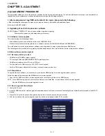
[1] ADJUSTMENT PROCEDURE

The adjustment values are set to the optimum conditions at the factory before shipping. If a value should become improper or an adjustment is
required due to part replacement, make an adjustment according to the following procedure.

1. After replacement of any PWB unit and/or IC for repair, please note the following.

 When replacing the following units, make sure to prepare the new units loaded with updated software.

MAIN Unit: DUNTKE716FM02

2. Upgrading of each microprocessor software

CAUTION: Never “POWER OFF” the unit when software upgrade is ongoing.

Otherwise the system may be damaged beyond recovery.

2.1. Software version upgrade

The model employs the following software.

• Main software (please use a software version after LAKEA200.USB.)

• Monitor microprocessor software (please use a software version after LAKEVA05.USB and LAKEM300.BIN.)

The main software, monitor microprocessor software can be upgraded by using a general-purpose USB Memory.

The followings are the procedures for upgrading, explained separately for the main software, monitor microprocessor software.

2.2. Main software version upgrade

2.2.1 Get ready before you start

• USB Memory of 128MB or higher capacity.

• PC running on Windows 98/98SE/ME/2000/XP operating system.

• USB Memory reader/writer or PC with a USB port.

• The file system of a USB memory is FAT. (FAT32 is not applied)

• Use the USB memory without other functions. (lock and memory reader...etc)

2.2.2 Preparations

To upgrade the main software, it is necessary to get ready the USB Memory for version upgrade before you start.

Follow the steps below and create the USB Memory for version upgrade.

1. Copy the file LAKEAxxx.USB for version upgrade to the root directory (folder) of the USB Memory.

NOTE: In the USB Memory drive, do not store other folders or unrelated files, or more than one file for version upgrade.

Now the USB Memory for version upgrade is ready.

2.2.3 How to upgrade the software

1. Unplug the AC cord.

2. Insert the USB Memory for version upgrade (prepared as above) into the service socket located Right side of Main Board terminals, under INPUT3

terminal.

3. Plug in the AC cord with power button pressed down after 5 seconds, unpress the power button.

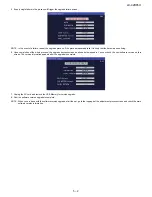
4. After the unit startup, the system upgrade screen as shown below appears within 20-40 seconds.

D65

Summary of Contents for LC42D65U - LC - 42" LCD TV

Page 1: ...OVING OF MAJOR PARTS 1 REMOVING OF MAJOR PARTS 4 1 CHAPTER 5 ADJUSTMENT 1 ADJUSTMENT PROCEDURE 5 1 2 PUBLIC MODE SETTING PROCEDURE 5 16 CHAPTER 6 TROUBLE SHOOTING TABLE 1 TROUBLE SHOOTING TABLE 6 1 CHAPTER 7 MAJOR IC INFORMATIONS 1 MAJOR IC INFORMATIONS 7 1 CHAPTER 8 OVERALL WIRING BLOCK DIAGRAM 1 OVERALL WIRING DIAGRAM 8 1 2 SYSTEM BLOCK DIAGRAM 8 2 CHAPTER 9 PRINTED WIRING BOARD ASSEMBLIES 1 KEY...

Page 2: ...e AC voltage drop across the resistor All checks must be repeated with the AC cord plug connection reversed If necessary a nonpolarized adaptor plug must be used only for the purpose of completing these checks Any reading of 0 75 Vrms this corresponds to 0 5 mA rms AC or more is excessive and indicates a potential shock hazard which must be corrected before returning the monitor to the owner SAFET...

Page 3: ...t de compartiment les réseaux de résistancecapacité les isolateurs mécaniques etc S assurer qu il n y ait pas de danger d électrocution en vérifiant la fuite de courant de la facon suivante Brancher le cordon d alimentation directem ent à une prise de cou rant de 110 240V Ne pas utiliser de transformateur d isolation pour cet essai A l aide de deux fils à pinces brancher une résistance de 1 5 kΩ 1...

Page 4: ...solder by 40 C and as it has poor solder wettability you may be apt to keep the soldering bit in contact with the PWB for extended period of time However Since the land may be peeled off or the maximum heat resistance temperature of parts may be exceeded remove the bit from the PWB as soon as you confirm the steady soldering condition Lead free solder contains more tin and the end of the soldering...

Page 5: ...ection management measures 1 When disposing of the component parts and PWBs destruct the IC itself in a proper way For repairing or replacing the component parts and PWBs as well as clearing those in stock 2 In storing the component parts protect and manage them against theft and disclosure For storing the service parts service units etc Applied part HDCP KEY ROM IC8451 RH IXC318WJQZY updated ROM ...

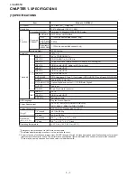
Page 6: ...ABLE AUDIO Audio in Ø 3 5 mm jack DIGITAL AUDIO OUTPUT Optical Digital audio output 1 PCM Dolby Digital OUTPUT Audio out RS 232C 9 pin D sub male connector Side INPUT 3 AV in INPUT 5 HDMI in with HDCP SERVICE Software update OSD language English French Spanish Power Requirement AC 120 V 60 Hz FOR NORTH AMERICA AC 110 240 V 50 60 Hz FOR OTHERS Power Consumption 235 W 0 4 W Standby with AC 120 V Wei...

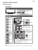
Page 7: ...32C terminal DIGITAL AUDIO OUTPUT terminal INPUT 7 terminal HDMI INPUT 9 terminal HDMI INPUT 8 terminal HDMI INPUT 6 terminal HDMI INPUT 4 terminal PC IN AUDIO terminal shared for INPUT 4 and INPUT 6 Antenna Cable in INPUT 1 terminals INPUT 2 terminals AUDIO OUTPUT terminals INPUT 3 terminals SERVICE terminal INPUT 5 terminal HDMI The illustrations in this operation manual are for explanation purp...

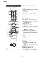
Page 8: ...o press FUNCTION and DISPLAY at the same time 18 LIGHT When this button is pressed some buttons for example VOL and CH on the remote control unit will light The lighting will turn off if no operations are performed within about 5 seconds This button is used for performing operations in low light situations 19 VIEW MODE Select the screen size 20 ENT Jumps to a channel after selecting with the 0_9 b...

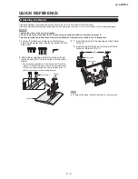
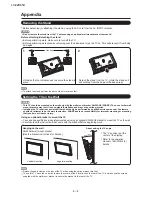
Page 9: ...etaching the stand unplug the AC cord from the AC INPUT terminal Before performing work spread cushioning over the base area to lay the TV on This will prevent it from being damaged QUICK REFERENCE To detach the stand perform the steps in reverse order 3 Insert the stand into the openings on the bottom of the TV Insert and tighten the 4 short screws into the 4 holes on the rear of the TV Forward H...

Page 10: ...pplied with the wall mount bracket to secure the bracket to the rear of the TV Setting the TV on the Wall CAUTION This TV should be mounted on the wall only with the wall mount bracket AN 52AG4 SHARP The use of other wall mount brackets may result in an unstable installation and may cause serious injuries Installing the TV requires special skill that should only be performed by qualified service p...

Page 11: ...cture may look dark in a room that is too bright Check the input signal setting Is the sleep timer set Check the power control settings The unit s internal temperature has increased Remove any objects blocking vent or clean Is connection to other components correct Is correct input signal source selected after connection Is the correct input selected Is picture adjustment correct Is On selected in...

Page 12: ...tion Setup Digital Caption Info Program Title Display Favorite CH Game Play Time Operation Lock Out Demo Mode Digital Setup Menu Audio Setup Identification Software Update On Screen Display Menu For TV INPUT 1 2 3 Mode For HDMI PC IN Mode Picture Menu OPC Backlight Contrast Brightness Color Tint Sharpness Advanced C M S Hue C M S Saturation Color Temp Active Contrast I P Setting Film Mode Digital ...

Page 13: ...vice Manual CHAPTER 3 DIMENSIONS 1 DIMENSIONS Unit inch mm 36 3 4 933 2 40 11 64 1020 25 9 16 649 28 1 32 712 20 23 32 526 16 17 64 413 4 13 16 122 3 61 64 100 12 13 16 325 21 21 32 550 2 17 32 64 15 3 4 400 7 7 8 200 15 3 4 400 ...

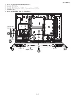
Page 14: ...TER 4 REMOVING OF MAJOR PARTS 1 REMOVING OF MAJOR PARTS 1 Remove the 4 lock screws and detach the Stand 2 Remove the 4 VESA Hole Covers 3 Remove the 1 lock screw 13 lock screws and detach the Rear Cabinet 3 3 2 1 Front Cabinet Rear Cabinet Stand ...

Page 15: ... Cover 5 Detach the KEY Unit Ass y 6 Detach the KEY Unit from the KEY Button Cover and disconnect KM Wire 7 Disconnect SP Wire 8 Remove the 2 lock screws and detach the Speaker LR SP 4 8 5 6 6 7 7 KM Bottom Cover Speaker L Speaker R KEY Unit KEY Button Cover SP 8 ...

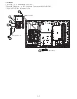
Page 16: ...ews and detach the Side AV Cover 10 Remove the 12 lock screws 4 lock Shafts 4 lock screws 2 lock screws and detach the Main Shield 11 Detach the R C LED Unit and disconnect RA Wire 10 10 10 10 Side AV Cover R C LED Unit Main Shield 9 11 RA ...

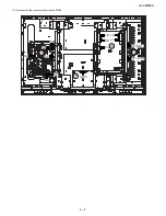
Page 17: ...LC 42D65U 4 4 12 Disconnect all the connectors from all the PWBs LB LB PD KM LW SP RA PD LA LA CN1 LC LC CN2 PL LW PL 12 12 12 12 ...

Page 18: ...LC 42D65U 4 5 13 Remove the 5 lock screws and detach the POWER Unit 14 Remove the 7 lock screws and detach the MAIN Unit Heat Sink Ass y 14 14 13 MAIN Unit Heat Sink Ass y POWER Unit ...

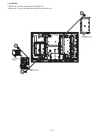
Page 19: ...w 2 lock screws and detach the POWER PWB Angle 19 Remove the 1 lock screw 1 lock screw and detach the Stand Angle B 20 Remove the 1 lock screw 1 lock screw and detach the Stand Angle A 21 Remove the 2 lock screws and detach the VESA Angle B 22 Remove the 2 lock screws and detach the VESA Angle A 15 16 17 15 MAIN PWB Angle Ass y Stand Angle B Stand Angle A POWER PWB Angle VESA Angle B POWER MAIN PW...

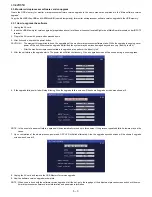
Page 20: ...ained separately for the main software monitor microprocessor software 2 2 Main software version upgrade 2 2 1 Get ready before you start USB Memory of 128MB or higher capacity PC running on Windows 98 98SE ME 2000 XP operating system USB Memory reader writer or PC with a USB port The file system of a USB memory is FAT FAT32 is not applied Use the USB memory without other functions lock and memory...

Page 21: ...success screen as shown below appears You can check the new software version on this screen The version information appears after the upgrade is complete 7 Unplug the AC cord and remove the USB Memory for version upgrade 8 Now the software version upgrade is complete NOTE When you are done with the software version upgrade start the set go to the top page of the adjustment process screen and check...

Page 22: ... recovery inability to start After the monitor microprocessor software is upgraded also perform the Industry Init 5 After the unit startup the upgrade starts The power led will blink continuously Also an upgrade screen will be shown during a minor upgrade 6 If the upgrade fails power led will stop blinking Also the upgrade failure screen will be shown if upgrade screen was shown at 5 NOTE In the e...

Page 23: ... described here lest your users should know how to enter the adjustment process mode If the settings are tampered in this mode unrecoverable system damage may result 4 Remote controller key operation and description of display in adjustment process mode 1 Key operation Input mode is switched automatically when relevant adjustment is started so far as the necessary input signal is available 2 Descr...

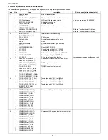
Page 24: ...setting for VIC READ 12 VIC SIGNAL TYPE Signal type setting for VIC READ 13 VIC READ Picture level acquisition function Level appears in green on the upper right 3 1 N358 ALL ADJ INPUT1 CVBS and TUNER signal level adjustment 2 N358 ALL ADJ INPUT3 3 N358 MAIN ADJ INPUT1 CVBS signal level adjustment 4 N358 MAIN ADJ INPUT3 5 TUNER DAC ADJ TUNER signal level adjustment 6 N358 CONTRAST A_GAIN 7 N358 CO...

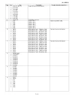
Page 25: ...djustment Point 3 R adjustment value 8 MG3G WB adjustment Point 3 G adjustment value 9 MG3B WB adjustment Point 3 B adjustment value 11 1 MG4R WB adjustment Point 4 R adjustment value Parameter for six point adjustment 2 MG4G WB adjustment Point 4 G adjustment value 3 MG4B WB adjustment Point 4 B adjustment value 4 MG5R WB adjustment Point 5 R adjustment value 5 MG5G WB adjustment Point 5 G adjust...

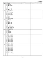
Page 26: ... PEQ3 F0 2 PEQ3 Q 3 PEQ3 Gain 4 PEQ3 Gain Limit 5 PEQ3 Fade Time 6 PEQ4 F0 7 PEQ4 Q 8 PEQ4 Gain 9 PEQ4 Gain Limit 10 PEQ4 Fade Time 19 1 PEQ5 F0 2 PEQ5 Q 3 PEQ5 Gain 4 PEQ5 Gain Limit 5 PEQ5 Fade Time 6 PEQ6 F0 7 PEQ6 Q 8 PEQ6 Gain 9 PEQ6 Gain Limit 10 PEQ6 Fade Time 20 1 PEQ7 F0 2 PEQ7 Q 3 PEQ7 Gain 4 PEQ7 Gain Limit 5 PEQ7 Fade Time 6 Subsonic Filter 21 1 Output Trim 2 Clipper 3 SubVolume Defaul...

Page 27: ...ase Time 9 BassAGC Threshold 10 BassAGC HPF F0 11 Bass Harmonics Level 12 Bass Harmonics LPF F 13 Bass Harmonics HPF F 25 1 PANNEL SELECT 2 PWM 3 PWM FREQ 4 PWM DUTY 5 OSC FREQ 6 OSC DUTY 26 1 BRIGHTNESS DA0 2 BRIGHTNESS DA1 3 BRIGHTNESS DA2 4 BRIGHTNESS DA3 5 BRIGHTNESS DA4 6 BRIGHTNESS DA5 7 BRIGHTNESS DA6 8 BRIGHTNESS DA7 9 BRIGHTNESS DA8 10 BRIGHTNESS DA9 11 BRIGHTNESS DA10 12 BRIGHTNESS DA11 ...

Page 28: ...3 ADLEVEL 16 6 OPC33 ADLEVEL 17 7 OPC33 ADLEVEL 18 8 OPC33 ADLEVEL 19 9 OPC33 ADLEVEL 20 10 OPC33 ADLEVEL 21 11 OPC33 ADLEVEL 22 31 1 OPC33 ADLEVEL 23 2 OPC33 ADLEVEL 24 3 OPC33 ADLEVEL 25 4 OPC33 ADLEVEL 26 5 OPC33 ADLEVEL 27 6 OPC33 ADLEVEL 28 7 OPC33 ADLEVEL 29 8 OPC33 ADLEVEL 30 9 OPC33 ADLEVEL 31 32 1 V6 OS THERMO 1 2 V6 OS THERMO 2 3 V6 OS THERMO 3 4 V6 OS THERMO 4 5 V6 OS THERMO 5 6 V6 OS T...

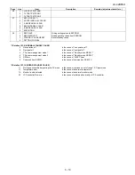
Page 29: ...n the cause of no signal off 4 PC power management mode 1 in the cause of Standby mode MODE1 5 PC power management mode 2 in the cause of Standby mode MODE2 6 Off timer in the cause of SLEEP timer 8 Command from RS232C in the cause of command by RS 232C 2 Details of P1 10 ERROR STANDBY CAUSE 11 Prolonged unspecified signal input in PC mode in the cause of continuous out of range PC input mode 17 T...

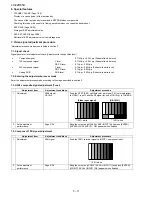
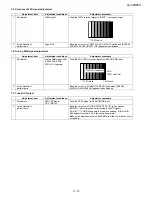
Page 30: ...02Vp p Pedestal to white level 15K component signal Y level 0 714Vp p 0 02Vp p Pedestal to white level PB PR level 0 7Vp p 0 02Vp p 33K component signal Y level 0 7Vp p 0 02Vp p Pedestal to white level PB PR level 0 7Vp p 0 02Vp p Analog RGB RGB level 0 7Vp p 0 02Vp p Pedestal to white level Adjustment item Adjustment conditions Adjustment procedure 1 Adjustment N358 signal US 10ch Feed the NTSC 3...

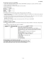
Page 31: ... separate Feed the XGA 100 color bar signal to ANALOG RGB input 2 Auto adjustment performance Bring the cursor on ANALOG RGB ADJ and press ENTER ANALOG RGB ADJ OK appears when finished Adjustment item Adjustment conditions Adjustment procedure 1 Adjustment NTSC RF signal US 7 AIR ch Feed the NTSC signal to RF ANTENNA input 2 Auto adjustment performance Bring the cursor on TUNER VCHIP TEST 07ch and...

Page 32: ...he G setting 428 x 6th point G setting 928 rounded off and make the R and B settings to their reference levels 6 Set the 2nd point to the specified gradation level Correct the G setting 348 x 6th point G setting 928 rounded off and make the R and B settings to their reference levels 7 Set the 1st point to the specified gradation level Correct the G setting 192 x 6th point G setting 928 rounded off...

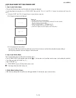
Page 33: ...g the channel settings are initialized Be cautious when making this adjust ment The adjustments done in the adjustment process mode are not initialized Baud rate 9 600 bps Data LENGTH 8 bit Parity bit None Stop bit 1 bit Flow control None Adjustment item Adjustment conditions Adjustment procedure 1 Initialization It turns off with AC power supply Enter the adjustment process mode Bring the cursor ...

Page 34: ...15WJQZY 㪛㪼㫊㫋㫀㫅㪸㫋㫀㫆㫅㩷㪠㪛㩷㪺㫆㫅㫅㪼㪺㫋㫆㫉㩷㫃㫆㪺㪸㫋㫀㫆㫅㫊 㪧㫃㫌㪾㩷㫃㫆㪺㪸㫋㫀㫆㫅㫊 㪛㪼㫊㫋㫀㫅㪸㫋㫀㫆㫅㩷㪠㪛㩷㪺㫆㫅㫅㪼㪺㫋㫆㫉 䋨㪨㪚㪥㪚㪮㪘㪎㪈㪌㪮㪡㪨㪱㪰䋩 㪛㪼㫊㫋㫀㫅㪸㫋㫀㫆㫅㩷㪠㪛㩷㫇㫃㫌㪾 䋨㪨㪚㪥㪚㪤㪘㪉㪎㪌㪮㪡㪨㪱䋩 㪣㪚㪄㪋㪉㪛㪍㪌㪬 㽲 㽶 㪪㪚㪐㪉㪇㪈 㪪㪚㪐㪉㪇㪉 㽲 㽴 㽶 㽳 㽸 㽹 㽵 㽷 㪙㪚㪤㪊㪌㪌㪊 䇼㪩㪘䇽 㪈㩷㩷㩷㩷㩷㩷㩷㪈㪇 㪈㩷㩷㪋 䇼㪪㪧䇽 䇼㪣㪮䇽 㪈 㪋㪈 䇼㪧㪛䇽 㪈 㪈㪉 䌈䌄䌍䌉 㪭㪆㪣㪩 㪟㪛㪤㪠 㪬㪪㪙 㪩㪪㪄㪉㪊㪉㪚 㪘㫅㪸㫃㫆㪾㩷㪩㪞㪙 㪧㪚㩷㪘㫌㪻㫀㫆㩷㪠㪥 䇼㪢㪤䇽 㪈 㪋 㪫㪬㪥㪜㪩 䇼㪣㪧䇽 㪈 㪈㪊 㪪㪚㪐㪉㪇㪉 㪪㪚㪐㪉㪇㪈 㪛㪛㪩 㪧㫆㫊㫀㫋㫀㫆㫅 Control tactile switch S terminal Optical output 㪣㪆㪩 Output ...

Page 35: ...to exit Public Mode There are the following ways to quit the public mode setup screen Turn off PUBLIC MODE in the adjustment process mode This way alone is not for quitting the setup screen but for quitting the mode itself Turn off the power with the POWER key Select EXECUTE PUBLIC MODE stays on in the adjustment process mode The settings will be back to the factory ones 3 Public Mode Setting Valu...

Page 36: ...r and VOL key remote controller and set To save new settings keep the cursor at EXECUTE and use ENTER key remote controller and set PUBLIC MODE POWER ON FIXED VARIABLE MAXIMUM VOLUME 60 VOLUME FIXED VARIABLE VOLUME FIXED LEVEL 20 RC BUTTON RESPOND PANEL BUTTON RESPOND MENU BUTTON RESPOND AV POSITION FIXED VARIABLE ON SCREEN DISPLAY YES INPUT MODE START NORMAL INPUT MODE FIXED VARIABLE LOUD SPEAKER...

Page 37: ...ecified for a fixed volume at start Limit in Setting The sound volume for the ON timer Wake up timer is fixed also without display of menu Besides the setting is made impossible Basically the menu is not displayed The following keys become invalid Sound volume Up Down VOL for both remote control and the unit Mute MUTE Exception In the item VOLUME of adjustment process the sound volume can be set f...

Page 38: ...yed This is because the channel call mes sage may be confused with a message being sent from the hotel On the North America destined models the OSD works the same as at the No setting Limit in Setting Keys falling under any of the following items become invalid Appearance of screen changes and the sound changes Personal functions which are hard to restore Screen display menu OFF timer ON timer AV ...

Page 39: ...ction between OFF ON TV RCE and ON TV RCD loop provided Default OFF Explanation Function to feed the remote controller received signal to Pin 9 open on the RS232C Limit in Setting None Exception None Remarks None Selection Selection between Variable and Fixed loop provided Default Variable Explanation In case of Fixed setting Menu Picture and Audio setting can t be changed like Dynamic Fixed When ...

Page 40: ...election Selection between ON and OFF loop provided Default OFF Explanation In case of ON public mode settings are effected Limit in Setting None Exception None Remarks The public mode settings are operable only when this item is set at ON ...

Page 41: ...1 CPU Check the line between pin 7 of input terminal J501 and pin J34 of IC8001 CPU Is there the COMPOSITE signal input at pin AN16 of IC8001 CPU Is there the COMPOSITE signal input at pin AN17 of IC8001 CPU YES NO YES NO Check the line between pin 3 of J507 and pin AN16 of IC8001 Check the line between pin 6 of J501 and pin AN17 of IC8001 Are the LVDS signal outputs at the LVDS 1st channel and 2n...

Page 42: ...COMPONENT video signal inputs at pins AM21 Y AN21 Pb and AL21 Pr of IC8001 CPU Are there the COMPONENT video signal inputs at pins AN22 Y AP22 Pb and AL22 Pr of IC8001 CPU YES NO YES NO Check the line between the input terminals of J508 and IC8001 J508 pin 3 Y pin 5 Pb pin 7 Pr IC8001 pin AM21 pin AN21 pin AL21 Check the line between the input terminals of J502 and IC8001 J508 pin 3 Y pin 5 Pb pin...

Page 43: ...en pins 3 Y 4 C of J504 and pins AN17 AN16 of IC8001 Q519 and Q520 etc Are the LVDS signal outputs at the LVDS 1st channel and 2nd channel of IC8001 LVDS_TX_0_DATA0_P N C7 B7 LVDS_TX_0_DATA1_P N E7 D7 LVDS_TX_0_DATA2_P N C6 B6 LVDS_TX_0_DATA3_P N C5 B5 LVDS_TX_0_DATA4_P N E5 D5 LVDS_TX_0_CLK_P N E6 D6 LVDS_TX_1_DATA0_P N B4 A4 LVDS_TX_1_DATA1_P N E4 D4 LVDS_TX_1_DATA2_P N B3 A3 LVDS_TX_1_DATA3_P N...

Page 44: ...re there the video signal inputs at pin AM33 and AM34 of IC8001 CPU YES NO YES NO Check the line between IC8001 and TU1101 and their periph eral circuits Q1103 etc Check the line between IC8001 and TU1101 and their periph eral circuits L1101 C1103 etc Are the LVDS signal outputs at the LVDS 1st channel and 2nd channel of IC8001 LVDS_TX_0_DATA0_P N C7 B7 LVDS_TX_0_DATA1_P N E7 D7 LVDS_TX_0_DATA2_P ...

Page 45: ...PU Are there the VSYNC HSYNC signal inputs at pins AJ16 and AH16 of IC8001 NO Check the line between SC1802 and IC8001 Q1805 thru Q1807 IC1802 etc YES Are the LVDS signal outputs at the LVDS 1st channel and 2nd channel of IC8001 LVDS_TX_0_DATA0_P N C7 B7 LVDS_TX_0_DATA1_P N E7 D7 LVDS_TX_0_DATA2_P N C6 B6 LVDS_TX_0_DATA3_P N C5 B5 LVDS_TX_0_DATA4_P N E5 D5 LVDS_TX_0_CLK_P N E6 D6 LVDS_TX_1_DATA0_P...

Page 46: ...en the pin 31 of IC1604 and the pin AF8 of IC8001 Check the line between the pin 31 of IC1604 and the pin AF8 of IC8001 Are there the TMDS signal inputs at pins 38 39 CLK 41 42 D0 44 45 D1 47 48 D2 all of IC1604 Are there the TMDS signal inputs at pins 53 54 CLK 56 57 D0 59 60 D1 62 63 D2 all of IC1604 YES NO YES NO Is IC1601 EEPROM accessed by I2C with HDMI connected to read the DDC_I2C SCL SDA d...

Page 47: ...n 31 of IC1804 and the pin AL2 of IC8001 Are there the TMDS signal inputs at pins 4 5 CLK 7 8 D0 10 11 D1 13 14 D2 all of IC1604 Are there the TMDS signal inputs at pins 38 39 CLK 41 42 D0 44 45 D1 47 48 D2 all of IC1804 YES NO YES NO Is IC1603 EEPROM accessed by I2C with HDMI connected to read the DDC_I2C SCL SDA data Is IC1805 EEPROM accessed by I2C with HDMI connected to read the DDC_I2C SCL SD...

Page 48: ... 62 63 D2 all of IC1804 YES NO Is IC1801 EEPROM accessed by I2C with HDMI connected to read the DDC_I2C SCL SDA data NO Check the DDC line and its peripheral circuits IC1801 and its peripherals Are there the TMDS signal inputs at pins AM1 AM2 CLK AN1 AN2 D0 AM3 AM4 D1 AP2 AN3 D2 all of IC8001 CPU YES NO Check IC1804 IC8001 and their peripheral circuits Are the LVDS signal outputs at the LVDS 1st c...

Page 49: ...of input termi nal J503 to pins 37 L and 38 R of IC1403 CODEC YES NO YES NO Check the line between J507 and IC1403 Check the line between J503 and IC1403 Does the I2S signal come from pins 4 COD_LRCK 5 COD_BCK and 6 COD_SDOUT of IC1403 to pins AK24 AH24 and AJ24 of IC8001 CPU YES NO Check the line between IC1403 and IC8001 Does the audio signal come from pins AP28 AN28 SPOUT_LN P and AN29 AP29 to ...

Page 50: ... I2S signal come from pins 4 COD_LRCK 5 COD_BCK and 6 COD_SDOUT of IC1403 to pins AK24 AH24 and AJ24 of IC8001 CPU YES NO Check the line between IC1403 and IC8001 Does the audio signal come from pins AP28 AN28 SPOUT_LN P and AN29 AP29 to pins 6 5 INLM INLP and 8 9 INRM INRP of IC2701 AMP NO Check the line between IC8001 and IC2701 and their periph eral circuits Q1306 thru Q1308 AMP_MUTE line etc Y...

Page 51: ...output selected for Digital on the menu screen Set the HDMI audio output to Analog Does the audio signal come from pins 2 L and 3 R of input terminal J1801 to pins 46 L and 47 R of IC1403 CODEC YES NO Check the line between J1801 and IC1403 and their peripheral circuits Does the I2S signal come from pins 4 COD_LRCK 5 COD_BCK and 6 COD_SDOUT of IC1403 to pins AK24 AH24 and AJ24 of IC8001 CPU NO Che...

Page 52: ...ral circuits Check TU1101 and its peripheral circuits SDA3 SCL3 etc Does the SIF signal come from pin 15 of tuner TU1101 to pin AN23 of IC8001 CPU Are there the video signal inputs at pin AM33 and AM34 of IC8001 CPU YES NO YES NO Check the line between TU1101 and IC8001 and their peripheral circuits Q1101 Q1102 etc Check the line between TU1101 and IC8001 and their peripheral circuits L1101 C1103 ...

Page 53: ...r to No external input video HDMI INPUT 5 INPUT 6 input If no video appears refer to No external input video HDMI INPUT 6 INPUT 7 input If no video appears refer to No external input video HDMI INPUT 7 INPUT 8 input If no video appears refer to No external input video HDMI INPUT 8 INPUT 9 input If no video appears refer to No external input video HDMI INPUT 9 YES Is the HDMI_MUTE line as specified...

Page 54: ...1 and IC8001 and their peripheral circuits L1101 C1103 etc Is there the SPDIF signal output OPT_OUT at pin AP11 of IC8001 CPU YES NO Check the IC8001 and its peripheral circuits Is there the SPDIF signal OPT_OUT input at pin 2 of IC1304 SPDIF_BUFF MUTE NO Check the line between IC8001 and IC1304 YES Is there the MUTE signal input at pin 1 of IC1304 NO Check the MUTE_A_ALL and AC_DET signals and th...

Page 55: ... there the audio signal outputs at pins 24 LINE_L and 25 LINE_R of IC1403 CODEC NO Check IC1403 and its peripheral circuits YES Does the audio signal come from pins 24 LINE_L and 25 LINE_R of IC1403 to pins 4 L and 2 R of J505 NO Check the line between IC1403 and J505 and their peripheral circuits Check the LINE_MUTE line and its peripheral circuits Q1310 thru Q1311 etc ...

Page 56: ...wice Refer to Power failure details Communication failure with main CPU Flashes 3 times Refer to Communication failure details Communication line failure or main CPU communication fail ure Check debug statements for the main CPU Vsync Failure Flashes 4 times VSYNC pin 73 failure uninput Operation failure Detected during operation interruption Detected during operation interruption Monitor temperat...

Page 57: ...displayed in ERROR STANDBY CAUSE on page 1 of process A for the main microprocessor LCD TCON ROM failure Flashes 8 times LCD TCON ROM Data error When this error occurs rewrite TCON ROM Data Error type Notification LED operation 1 cycle Basically communication logs are analyzed by a bus monitor or debug print logs are analyzed Initial communication reception failure Flashes once Initial communicati...

Page 58: ...sport processor a digital audio processor a high definition HD MPEG video decoder 2D graphics processing digital processing of analog video and audio analog video digitizer and DAC functions stereo high fidelity audio DACs two HDMI receivers for 1080p 60 inputs a 330 MHz millions of instructions per second MIPS processor and a peripheral control unit providing a variety of television control funct...

Page 59: ...he 256M bit page mode flash memory device stores the main CPU program 1 9 IC9003 VHiM3221EiP 1Y This IC is a single driver single receiver RS 232 solution operating from a single Vcc supply The device provides the electrical interface between an asynchronous communication controller and the serial port connector The IC has the function of Auto Power down By this function drivers are disabled autom...

Page 60: ...LC 42D65U 7 3 MEMO ...

Page 61: ... 㪩㪛㪜㪥㪚㪘㪉㪐㪏㪮㪡㪨㪱 䇼㪩㪘䇽 㪈 㪈㪇 㪈㩷㩷㪋 䇼㪪㪧䇽 㪩㪪㪄㪉㪊㪉㪚 㪣㪆㪩㩷㫆㫌㫋 㪘㫅㪸㫃㫆㪾㩷㪩㪞㪙 㪧㪚㩷㪘㫌㪻㫀㫆㩷㪠㪥 㩷 㪪㩷㫋㪼㫉㫄㫀㫅㪸㫃 㪦㫇㫋㫀㪺㪸㫃㩷㫆㫌㫋 䇼㪣㪮䇽 㪈 㪋㪈 䇼㪧㪛䇽 㪈 㪈㪉 䇼㪢㪤䇽 㪈 㪋 䇼㪢㪤䇽 㪈 㪌 㪈 㪈㪉 㪈 㪋 㪣㪚㪛㩷㪚㫆㫅㫋㩷㪬㫅㫀㫋 㪈㩷㩷㩷㩷㩷㩷㩷㩷㪏㪇 㪈㩷㩷㩷㩷㩷㩷㩷㩷㪏㪇 㪈㩷㩷㩷㩷㩷㩷㩷㩷㪌㪈 䇼㪩㪘䇽 㪈㩷㩷㩷㩷㩷㩷㪈㪇 㪫㪬㪥㪜㪩 㪣㪜㪛㩷㪬㫅㫀㫋 㪜㪏㪍㪏㪝㪤㪇㪈 㪈 㪍 㪈 㪈㪉 䇼㪣㪘㪉䇽 䇼㪣㪧䇽 㪈 㩷 㪈㪋 㪢㪜㪰㩷㪬㫅㫀㫋 㪜㪉㪍㪍㪝㪤㪇㪉 㪈 㪈㪊 㪈 㪈㪇 䇼㪣㪘㪈䇽 㪈 㪋 䇼㪣㪙㪈䇽 㪩㪈㪣㪢㪋㪉㪇㪛㪊㪣㪝㪉㪈㪱 䇼㪚㪥㪈䇽 䇼㪚㪥㪉䇽 㪈 㪉 㪈 㪉 㪧㪛㩷㪑㩷㪨㪚㪥㪮㪄㪟㪌㪈㪏㪮㪡㪨㪱 㪣㪧㩷㪑㩷㪨㪚㪥㪮㪄㪟㪌㪈㪍㪮㪡㪨㪱 㪣㪘㪈㩷㪑㩷㪨㪚㪥㪮㪄㪟㪌㪈㪌㪮㪡㪨㪱 㪣...

Page 62: ...Z 6Z VCN 5 VCN 241 5 5 7 8 8 0276 0276 0276 8 5 4 QORQPGPV 4 0 67 PCNQI KIKVCN 6WPGT A 8 6Z 4Z 56 A 27 56 TQO 27 41 5 8 A 8 4GUGV 7 8 176 0A456A 1 1 A 4 1 A 52A5 0 1 A5 176 75 20 A10 TQO 27 㪠㪚㪐㪇㪇㪊 㪩㪪㪉㪊㪉㪚㩷㪫㫏㪩㫏 㪤㪊㪉㪉㪈㪜㪠㪧 45 8 0Q RKP 4 2CUUVJTQWIJ 6A 8 6A 8 6 6 6A20 8 241 7 8 8 5 ޣ 9 ޤ 2 R 2 ޣ 2 ޤ 2 RKP 59 20 A A 0 8 8 8 241 2 8 241 MDKV 8 8 8 5 QORQPGPV 8 5 4 0276 0276 2D2T 8 5 4 4 8 A 4 4 8 A 4 VCN ...

Page 63: ... CHAPTER 9 PRINTED WIRING BOARD ASSEMBLIES 1 KEY Unit A C B D E F G I H 1 2 3 4 5 6 7 8 9 10 11 12 13 14 15 16 17 18 19 20 21 22 KEY Unit Side A KEY Unit Side A Chip S155 R153 D152 S154 S152 R151 D151 S151 R152 S153 R154 S156 S157 D155 P151 ...

Page 64: ...LC 42D65U 9 2 2 MAIN Unit A C B D E F G I H 1 2 3 4 5 6 7 8 9 10 11 12 13 14 15 16 17 18 19 20 21 22 MAIN Unit Side A ...

Page 65: ... R1650 R1652 R1646 R1648 R1666 IC1604 R1667 L1601 SC1602 L1602 L1603 L1604 R1651 R1862 R1865 R1866 R1867 R1856 R1855 L1802 IC1804 SG1801 SG1803 SG1805 SG1807 SG1802 SG1804 SG1806 SG1808 L1803 L1804 TP8095 TP8093 TP8097 L1805 TP8094 TP8092 TP8096 R1868 TP8012 TP8045 TP8051 TP8011 TP8015 TP8048 SC1801 TP8014 TP8099 TP8013 TP8098 R8146 R8144 R8022 R8909 C8124 C8122 C8123 C8121 LUG1110 R8053 C8130 R80...

Page 66: ...LC 42D65U 9 4 A C B D E F G I H 1 2 3 4 5 6 7 8 9 10 11 12 13 14 15 16 17 18 19 20 21 22 MAIN Unit Side B ...

Page 67: ...801 C1838 C1830 C1834 R1858 R1860 R1872 C1803 C1831 C1835 R1871 FB1810 R1811 R1810 TL1608 TL1612 D1611 R1634 Q1611 R1861 R1863 IC1602 R1630 R1618 R1627 D1613 C1611 TL1605 TL1614 R1668 R1657 C1609 TL1618 R1645 R1644 R1665 R1664 C1636 R1643 R1642 R1629 TL1616 IC1605 C1605 C1606 C1628 C1604 C1633 FB1604 C1623 C1624 C1627 C1603 R1638 R1639 D1607 D1604 C1622 C1621 R1640 R1641 C1613 C1631 C1632 IC1606 R...

Page 68: ... H 1 2 3 4 5 6 7 8 9 10 11 12 13 14 15 16 17 18 19 20 21 22 R C LED Unit Side A R C LED Unit Side A Chip R103 P101 C102 IC101 R105 C101 R107 R106 Q102 R108 D102 R109 Q104 R104 R110 Q103 3 R101 Q101 D101 D103 R102 RMC101 SLD101 R111 C104 C103 LF3 ...

Page 69: ...F unless otherwise noted P pF µµF 2 All capacitors are 50V unless otherwise noted CAUTION This circuit diagram is original one therefore there may be a slight difference from yours SAFETY NOTES 1 DISCONNECT THE AC PLUG FROM THE AC OUTLET BEFORE REPLACING PARTS 2 SEMICONDUCTOR HEAT SINKS SHOULD BE REGARDED AS POTENTIAL SHOCK HAZARDS WHEN THE CHASSIS IS OPERATING IMPORTANT SAFETY NOTICE PARTS MARKED...

Page 70: ...LC 42D65U 10 2 2 KEY Unit A C B D E F G I H 1 2 3 4 5 6 7 8 9 10 11 12 13 14 15 16 17 18 19 20 21 22 ...

Page 71: ...LC 42D65U 10 3 3 MAIN Unit MAIN Unit 1 17 A C B D E F G I H 1 2 3 4 5 6 7 8 9 10 11 12 13 14 15 16 17 18 19 20 21 22 ...

Page 72: ...LC 42D65U 10 4 MAIN Unit 2 17 A C B D E F G I H 1 2 3 4 5 6 7 8 9 10 11 12 13 14 15 16 17 18 19 20 21 22 ...

Page 73: ...LC 42D65U 10 5 MAIN Unit 3 17 A C B D E F G I H 1 2 3 4 5 6 7 8 9 10 11 12 13 14 15 16 17 18 19 20 21 22 ...

Page 74: ...LC 42D65U 10 6 MAIN Unit 4 17 A C B D E F G I H 1 2 3 4 5 6 7 8 9 10 11 12 13 14 15 16 17 18 19 20 21 22 ...

Page 75: ...LC 42D65U 10 7 MAIN Unit 5 17 A C B D E F G I H 1 2 3 4 5 6 7 8 9 10 11 12 13 14 15 16 17 18 19 20 21 22 ...

Page 76: ...LC 42D65U 10 8 MAIN Unit 6 17 A C B D E F G I H 1 2 3 4 5 6 7 8 9 10 11 12 13 14 15 16 17 18 19 20 21 22 ...

Page 77: ...LC 42D65U 10 9 MAIN Unit 7 17 A C B D E F G I H 1 2 3 4 5 6 7 8 9 10 11 12 13 14 15 16 17 18 19 20 21 22 ...

Page 78: ...LC 42D65U 10 10 MAIN Unit 8 17 A C B D E F G I H 1 2 3 4 5 6 7 8 9 10 11 12 13 14 15 16 17 18 19 20 21 22 ...

Page 79: ...LC 42D65U 10 11 MAIN Unit 9 17 A C B D E F G I H 1 2 3 4 5 6 7 8 9 10 11 12 13 14 15 16 17 18 19 20 21 22 ...

Page 80: ...LC 42D65U 10 12 MAIN Unit 10 17 A C B D E F G I H 1 2 3 4 5 6 7 8 9 10 11 12 13 14 15 16 17 18 19 20 21 22 ...

Page 81: ...LC 42D65U 10 13 MAIN Unit 11 17 A C B D E F G I H 1 2 3 4 5 6 7 8 9 10 11 12 13 14 15 16 17 18 19 20 21 22 ...

Page 82: ...LC 42D65U 10 14 MAIN Unit 12 17 A C B D E F G I H 1 2 3 4 5 6 7 8 9 10 11 12 13 14 15 16 17 18 19 20 21 22 ...

Page 83: ...LC 42D65U 10 15 MAIN Unit 13 17 A C B D E F G I H 1 2 3 4 5 6 7 8 9 10 11 12 13 14 15 16 17 18 19 20 21 22 ...

Page 84: ...LC 42D65U 10 16 MAIN Unit 14 17 A C B D E F G I H 1 2 3 4 5 6 7 8 9 10 11 12 13 14 15 16 17 18 19 20 21 22 ...

Page 85: ...LC 42D65U 10 17 MAIN Unit 15 17 A C B D E F G I H 1 2 3 4 5 6 7 8 9 10 11 12 13 14 15 16 17 18 19 20 21 22 ...

Page 86: ...LC 42D65U 10 18 MAIN Unit 16 17 A C B D E F G I H 1 2 3 4 5 6 7 8 9 10 11 12 13 14 15 16 17 18 19 20 21 22 ...

Page 87: ...LC 42D65U 10 19 MAIN Unit 17 17 A C B D E F G I H 1 2 3 4 5 6 7 8 9 10 11 12 13 14 15 16 17 18 19 20 21 22 ...

Page 88: ...LC 42D65U 10 20 4 R C LED Unit A C B D E F G I H 1 2 3 4 5 6 7 8 9 10 11 12 13 14 15 16 17 18 19 20 21 22 ...

Page 89: ...e subject to change without notice LC 42D65U Note The reference numbers on the PWB are arranged in alphabetical order No S78N2LC42D65U LC 42D65U MODEL PartsGuide 1 PRINTED WIRING BOARD ASSEMBLIES 2 LCD PANEL NOTE THE PARTS HERE SHOWN ARE SUPPLIED AS AN ASSEMBLY BUT NOT INDEPENDENTLY 3 DUNTKE266FM02 KEY Unit 4 DUNTKE716FM02 MAIN Unit 5 DUNTKE868FM01 R C LED Unit 6 CABINET AND MECHANICAL PARTS 7 SUP...

Page 90: ...CCZ1HH150JY AB J Capacitor 15p 50V Ceramic C522 VCCCCZ1HH150JY AB J Capacitor 15p 50V Ceramic C523 VCCCCZ1HH150JY AB J Capacitor 15p 50V Ceramic C525 VCCCCZ1HH150JY AB J Capacitor 15p 50V Ceramic C533 VCCCCZ1HH471JY AA J Capacitor 470p 50V Ceramic C535 VCKYCY1AB105KY AB J Capacitor 1 10V Ceramic C536 VCCCCZ1HH471JY AA J Capacitor 470p 50V Ceramic C537 VCCCCZ1HH471JY AA J Capacitor 470p 50V Ceramic...

Page 91: ...04KY AB J Capacitor 0 1 10V Ceramic C1624 VCKYCZ1HB102KY AB J Capacitor 1000p 50V Ceramic C1625 RC KZA520WJQZY AA J Capacitor 1 10V Ceramic C1627 VCKYCZ1AB104KY AB J Capacitor 0 1 10V Ceramic C1628 VCKYCZ1HB102KY AB J Capacitor 1000p 50V Ceramic C1629 VCKYCZ1AB104KY AB J Capacitor 0 1 10V Ceramic C1630 VCKYCZ1HB102KY AB J Capacitor 1000p 50V Ceramic C1631 VCKYCZ1AB104KY AB J Capacitor 0 1 10V Cera...

Page 92: ...Y AB J Capacitor 1 25V Ceramic C2725 VCKYCY1EB104KY AB J Capacitor 0 1 25V Ceramic C2726 VCKYCY1EB104KY AB J Capacitor 0 1 25V Ceramic C2727 VCKYCY1EB104KY AB J Capacitor 0 1 25V Ceramic C2728 VCKYCY1EB104KY AB J Capacitor 0 1 25V Ceramic C2730 VCKYTV1EB224KY AA J Capacitor 0 22 25V Ceramic C2731 VCKYTV1EB224KY AA J Capacitor 0 22 25V Ceramic C2737 VCCCCZ1HH151JY AB J Capacitor 150p 50V Ceramic C2...

Page 93: ...eramic C8076 RC KZA510WJPZY AB J Capacitor 10 16V Ceramic C8077 VCKYCZ1AB104KY AB J Capacitor 0 1 10V Ceramic C8078 VCKYCZ1AB104KY AB J Capacitor 0 1 10V Ceramic C8079 VCKYCZ1AB104KY AB J Capacitor 0 1 10V Ceramic C8081 VCKYCZ1EB103KY AA J Capacitor 0 01 25V Ceramic C8082 RC KZA510WJPZY AB J Capacitor 10 16V Ceramic C8083 VCKYCZ1EB103KY AA J Capacitor 0 01 25V Ceramic C8084 VCKYCZ1EB103KY AA J Cap...

Page 94: ...04KY AB J Capacitor 0 1 10V Ceramic C8168 VCKYCZ1HB471KY AB J Capacitor 470p 50V Ceramic C8169 VCKYCZ1AB104KY AB J Capacitor 0 1 10V Ceramic C8170 VCKYCZ1HB471KY AB J Capacitor 470p 50V Ceramic C8172 RC KZA510WJPZY AB J Capacitor 10 16V Ceramic C8174 VCKYCZ1AB104KY AB J Capacitor 0 1 10V Ceramic C8175 VCKYCZ1AB104KY AB J Capacitor 0 1 10V Ceramic C8176 VCKYCZ1EB103KY AA J Capacitor 0 01 25V Cerami...

Page 95: ...1AB104KY AB J Capacitor 0 1 10V Ceramic C9601 VCCCCZ1HH101JY AB J Capacitor 100p 50V Ceramic C9602 VCKYCZ1HB681KY AB J Capacitor 680p 50V Ceramic C9603 VCKYCZ1EB472KY AB J Capacitor 4700p 25V Ceramic C9604 VCCCCZ1HH101JY AB J Capacitor 100p 50V Ceramic C9605 VCKYCZ1AB104KY AB J Capacitor 0 1 10V Ceramic C9606 VCKYCZ1EB103KY AA J Capacitor 0 01 25V Ceramic C9607 VCKYCY1EB104KY AB J Capacitor 0 1 25...

Page 96: ...J Diode 1SS226 T5L F T D1813 VHD1SS226 1Y AC J Diode 1SS226 T5L F T D1814 VHDMA111G 1Y AA J Diode MA2J1110GL D1815 VHDMA152WK 1Y AB J Diode MA152WK TX D1816 VHDMA111G 1Y AA J Diode MA2J1110GL D1817 VHD1SS226 1Y AC J Diode 1SS226 T5L F T D1818 VHD1SS226 1Y AC J Diode 1SS226 T5L F T D8002 RH PXA018WJZZY AC J Diode GM1HD55200A D9001 VHDMAZ9120H 1Y AC J Diode MAZ91200H0L D9002 VHDMA111G 1Y AA J Diode ...

Page 97: ...WJZZY AA J Ferrite Core FB2612 RBLN A074WJZZY AA J Ferrite Core FB2613 RBLN A074WJZZY AA J Ferrite Core FB2614 RBLN A074WJZZY AA J Ferrite Core FB2616 RBLN A074WJZZY AA J Ferrite Core FB2617 RBLN A074WJZZY AA J Ferrite Core FB2618 RBLN A074WJZZY AA J Ferrite Core FB2619 RBLN A074WJZZY AA J Ferrite Core FB2620 RBLN A074WJZZY AA J Ferrite Core FB2621 RBLN A074WJZZY AA J Ferrite Core FB2622 RBLN A074...

Page 98: ...TP D43 C IC8155 RH IXA361WJZZY AM J IC LP2995MX NOPB IC8451 RH IXC318WJQZY AL X IC IS24CO8A 2GLI IC8452 VHIS29GL1282EQ AX J IC BQC PROGRAM IC8454 VHIS24CS64A 1Y AF J IC S 24CS64AOI J8T1G IC9001 VHITC7W00U 1Y AE J IC TC7W00FU TE12L F IC9002 VHI7WH126FU 1Y AE J IC TC7WH126FU TE12L F IC9003 VHIM3221EIP 1Y AK J IC MAX3221EIPWR IC9004 VHILCX157FT 1Y AD J IC TC74LCX157FT EKJ IC9301 VHIAHC1G08W 1Y AD J I...

Page 99: ... J Transistor IMH23T110 Q1312 VSKRC404E 1Y AB J Transistor Q1601 VSRN1904 1Y AC J Transistor RN1904 TE85L F Q1602 VSRN1904 1Y AC J Transistor RN1904 TE85L F Q1603 VSRN1904 1Y AC J Transistor RN1904 TE85L F Q1604 VSRN1904 1Y AC J Transistor RN1904 TE85L F Q1605 VSRN1904 1Y AC J Transistor RN1904 TE85L F Q1606 VSRN1904 1Y AC J Transistor RN1904 TE85L F Q1610 VSRN4983 1Y AC J Transistor RN4983 TE85L ...

Page 100: ...tal Oxide R1103 VRS CZ1JF683JY AA J Resistor 68k 1 16W Metal Oxide R1107 VRS CZ1JF101JY AA J Resistor 100 1 16W Metal Oxide R1108 VRS CZ1JF101JY AA J Resistor 100 1 16W Metal Oxide R1109 VRS CZ1JF331JY AA J Resistor 330 1 16W Metal Oxide R1111 VRS CZ1JF203JY AA J Resistor 20k 1 16W Metal Oxide R1112 VRS CZ1JF151JY AA J Resistor 150 1 16W Metal Oxide R1113 VRS CZ1JF123JY AA J Resistor 12k 1 16W Met...

Page 101: ...S CZ1JF473FY AA J Resistor 47k 1 16W Metal Oxide R1631 VRS CZ1JF473FY AA J Resistor 47k 1 16W Metal Oxide R1632 VRS CZ1JF473FY AA J Resistor 47k 1 16W Metal Oxide R1633 VRS CZ1JF100JY AA J Resistor 10 1 16W Metal Oxide R1634 VRS CZ1JF100JY AA J Resistor 10 1 16W Metal Oxide R1635 VRS CZ1JF103JY AA J Resistor 10k 1 16W Metal Oxide R1636 VRS CZ1JF331JY AA J Resistor 330 1 16W Metal Oxide R1640 VRS C...

Page 102: ...tor 47k 1 16W Metal Oxide R1880 VRS CZ1JF473FY AA J Resistor 47k 1 16W Metal Oxide R1881 VRS CZ1JF473FY AA J Resistor 47k 1 16W Metal Oxide R1882 VRS CZ1JF100JY AA J Resistor 10 1 16W Metal Oxide R1883 VRS CZ1JF100JY AA J Resistor 10 1 16W Metal Oxide R2001 VRS CZ1JF101JY AA J Resistor 100 1 16W Metal Oxide R2002 VRS CZ1JF104JY AA J Resistor 100k 1 16W Metal Oxide R2003 VRS CZ1JF102JY AA J Resisto...

Page 103: ... Resistor 47 1 16W Metal Oxide R8016 VRS CZ1JF470JY AA J Resistor 47 1 16W Metal Oxide R8018 VRS CZ1JF472JY AA J Resistor 4 7k 1 16W Metal Oxide R8019 VRS CZ1JF470JY AA J Resistor 47 1 16W Metal Oxide R8020 VRS CZ1JF101JY AA J Resistor 100 1 16W Metal Oxide R8021 VRS CZ1JF750JY AA J Resistor 75 1 16W Metal Oxide R8023 VRS CZ1JF103JY AA J Resistor 10k 1 16W Metal Oxide R8025 VRS CZ1JF103JY AA J Res...

Page 104: ... CZ1JF220JY AA J Resistor 22 1 16W Metal Oxide R8183 VRS CZ1JF220JY AA J Resistor 22 1 16W Metal Oxide R8184 VRS CZ1JF220JY AA J Resistor 22 1 16W Metal Oxide R8185 VRS CZ1JF220JY AA J Resistor 22 1 16W Metal Oxide R8186 VRS CG1JF680JY AA X Resistor 68 1 16W Metal Oxide R8187 VRS CG1JF680JY AA X Resistor 68 1 16W Metal Oxide R8188 VRS CG1JF680JY AA X Resistor 68 1 16W Metal Oxide R8189 VRS CG1JF68...

Page 105: ...etal Oxide R8271 VRS CZ1JF000JY AA J Resistor 0 1 16W Metal Oxide R8452 VRS CZ1JF000JY AA J Resistor 0 1 16W Metal Oxide R8454 VRS CZ1JF000JY AA J Resistor 0 1 16W Metal Oxide R8456 VRS CZ1JF470JY AA J Resistor 47 1 16W Metal Oxide R8457 VRS CZ1JF470JY AA J Resistor 47 1 16W Metal Oxide R8474 VRS CZ1JF470JY AA J Resistor 47 1 16W Metal Oxide R8475 VRS CZ1JF470JY AA J Resistor 47 1 16W Metal Oxide ...

Page 106: ...33k 1 16W Metal Oxide R9740 VRS CZ1JF273JY AA J Resistor 27k 1 16W Metal Oxide R9741 VRS CZ1JF473FY AA J Resistor 47k 1 16W Metal Oxide SC1601 QSOCZA149WJQZY AF J Socket 23pin SC1602 QSOCZA171WJZZY AF N J Socket 23pin SC1603 QSOCZA171WJZZY AF N J Socket 23pin SC1801 QSOCZA171WJZZY AF N J Socket 23pin SC1802 QSOCNA770WJZZ AG J Socket 17pin SC1804 QSOCZA171WJZZY AF N J Socket 23pin SC9001 QSOCNA769W...

Page 107: ...G D T D102 RH PX0421CEZZY AD J Diode CL 165HR YG D T D103 RH EXA092WJZZY AB J Zener Diode UDZSFVTE 1712B IC101 VHIGA1S100W 1Y AE J IC GA1A1S100WP P101 QPLGNA330WJZZY AD J Plug 10pin RA Q101 VS2SC3928AR 1Y AB J Transistor 2SC3928A T112 1R Q102 VS2SC3928AR 1Y AB J Transistor 2SC3928A T112 1R Q103 VS2SC3928AR 1Y AB J Transistor 2SC3928A T112 1R Q104 VS2SC3928AR 1Y AB J Transistor 2SC3928A T112 1R R10...

Page 108: ... 6 6 6 52 47 2 2 1 2 2 36 38 42 35 37 50 22 14 48 50 49 49 25 27 26 9 50 28 50 50 50 51 24 54 17 31 33 34 50 5 5 1 5 2 49 16 15 58 49 15 48 48 20 49 13 49 20 48 48 19 18 11 12 21 50 44 7 45 23 23 29 29 32 52 41 POWER Unit MAIN Unit KEY Unit R C LED Unit 49 48 18 10 18 50 30 43 29 56 57 57 55 55 55 ...

Page 109: ... 20 LHLDWA175WJUZ AC J Wire Holder x5 21 LHLDWA176WJUZ AC J Wire Holder x4 22 LHLDZA506WJKZ AC N X POWER PWB Spacer x2 23 LX HZA003WJFN AC J Screw for SP x2 24 NSFTZA284WJFW AC N X Shaft x4 25 PCLICA004WJKZ AC J Rivet x3 26 PRDARA510WJFW AX J Radiator 27 PRDARA618WJFW AL X Heat Sink 28 PSLDMB421WJM1 AQ X Main Shield Ass y 29 PSLDMB506WJZZ AD N X Shield x3 30 PSPAZB570WJKZ AG J Cool Sheet 31 PSPAZB...

Page 110: ... RRMCGA724WJSA AX N X Remote Control Unit X5 TCADEA243WJZZ AD X Enquete Card X6 Not Available N Transition Note X7 Not Available Extend Warranty X8 TINS D779WJZZ AN N X Operation Manual X9 Not Available N AAA Size Battery X10 CDAI A418WJ36 BQ X Stand Unit X10 1 CX BZA208WJ01 AM X Stand Screw Ass y AAA Size Battery Remote Control Unit X4 Cable Clamp X2 Cable Band X1 AC Cord X3 X9 Operation Manual X...

Page 111: ...LC 42D65U 23 8 PACKING PARTS NOT REPLACEMENT ITEM S1 S2 S7 S8 S3 S5 S6 S6 S6 S6 S10 S4 S9 ...

Page 112: ...FOR SERVICING N QCNW G401WJQZ AP J Connecting Cord 4pin L 1000mm N MAIN to KEY Unit KM N QCNW H184WJQZ AX N J Connecting Cord 12pin L 1000mm N MAIN to POWER Unit PD N QCNW H649WJPZ AP J Connecting Cord 4pin L 1000mm N MAIN Unit to SPEAKER SP N QCNW H759WJQZ AP N J Connecting Cord 13pin L 1000mm N MAIN to POWER Unit LP LB1 N QCNW H760WJQZ AW N J Connecting Cord 10pin L 1000mm N POWER to INVERTER Un...

Page 113: ...tored in a retrieval system or transmitted in any form or by any means electronic mechanical photocopying recording or otherwise without prior written permission of the publisher COPYRIGHT XXXX BYSHARP CORPORATION ALL RIGHTS RESERVED MEMO LC 42D65U ...

Page 114: ... S MI KD COPYRIGHT 2008 BY SHARP CORPORATION ALL RIGHTS RESERVED No part of this publication may be reproduced stored in a retrieval system or transmitted in any form or by any means electronic mechanical photocopying recording or otherwise without prior written permission of the publisher LC 42D65U ...

Reviews: