


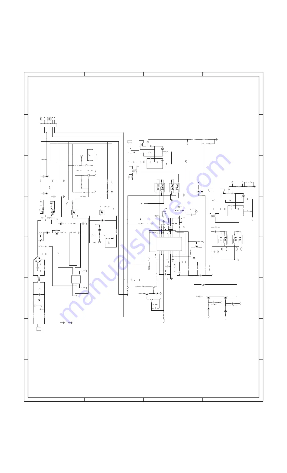
LL-T15S3
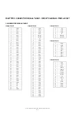
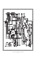
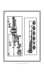
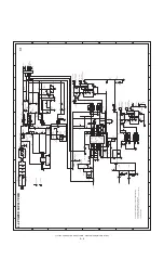
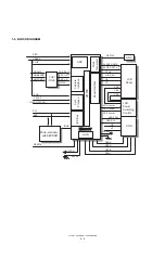
CONNECTOR SIGNAL TABLE • CIRCUIT DIAGRAM • PWB LAYOUT
5 – 6
Vhigh-2(Lamp2)
Vhigh-1(Lamp1)
Vlow-1(Lamp1)
Vlow-2(Lamp2)
Vhigh-2(Lamp2)
Vhigh-1(Lamp1)
Vlow-1(Lamp1)
Vlow-2(Lamp2)
R68,R71,R69,R72,R64,R65,R67,R83,R80(0
805) 0R
T
0
-220F
TO
-9
2
1/
8W
12.5*
2
0
1W
S
10*1
6
DO4
1
1/
8W
10R
(1
/4
W)
DR 8
*1
0
0.39
EFD
2
5
Fosc=5
0KHz
470U/25V(KY)
5*
1
1
1/
8W
10*1
6
TO
-9
2
1/
8W
1/
8W
1/
4W
DR 8
*1
0
1/
8W
13.
7K
R5
7
24.
9
K
105
K
1K
Primary GND
Secondary GND
R66,R67,R70,R79,R81,R84 (1206)
0R
J8,J9,J10,J11,J12,J13,J14,J15,J16,J17,J18,J19,
J20,J21
J22,J25,J26,J28
Y3
100U/
400V
(K
MG)
1M
18*
3
2
UU1
5
.7
10N 471
1000
P
1
0
00P
EN_ON
BRIGHTNESS
GND
+12V/2.0A
GND
+5V/1.8A
BRIGHTNESS
EN
_
O
N
+5V
RT
+5V
RT
CP
CP
CP
B+
B+
B+
TP
TP
TP
TP
TP
TP
TP
TP
CP
CP
CP
Pi
n
2
L1
2
1
3
4
Q9
SI4532
1
2
3
4
8
7
6
5
CN3
SM02B-BHSS-1-TB(JST)
2
1
U4
PC
-6
21
1
2
3
4
C39
101P/1KV
R42
R26
10K
R55
1
/4W
820
C45
4.7u/10V(X5R)1206
D13
EG
P1
0
M
2
1
C8 10n
C5
0.47U
R49
1K(1/8
W
)
R52
1/4
W 1
0
0
R54 1/
4W
5.
6K
C52
470n
R31
422R/1%
C46
4.7u/10V(X5R/1206)
C32
560pF(N
PO
)
D19
P6KE
160
A
2
1
ZD7
1/
2W
6B
2
21
R30
560R(1206)
R25
10K
R73
1/
8W
R50
1/4
W1
0
0
D18
P6KE
160
A
2
1
R48
100
K
ZD1
5.6v
F1
3A/DIP(R25103)
C35
0.1uf
Q4
MMBT3
90
4
1
2
3
R5
6
L4
12
C41
2n2/500V
T3
11
0
2
3 4
5
7
9
8
6
C3 10n
T1
19:2600
5,6,7
8
1,2,3,4
9
R74
1/
8W
C11
OPEN
ZD3
5.6v
D2
LL41
4
8
2
1
Q2
DTA114EKA
D1
LL414
8
2
1
R1
910R/1206
C47
100n(0805)
C28
4.7U,X5R,10V(1206)
R13
280K,1%
ZD4
5.6v
R76
1/
2W
1k
U5
T
L431
3
1
2
+
C38
1000uF/25V(KY)
C37
2n2/500V
+
C33
C16 0.047U
C29
15P,3KV
C6
1.0U/25V/1206
R8 1M
C10
C/NC
C31
6.8nF
C12 0.22U
R16
10K
R27 1M
Q10
SI4532
1
2
3
4
8
7
6
5
F2
F
U
S
E
- 2A
/250V
F
U
S
E
- 2A
/250V
12
Q5
2N7002
2
3
1
+
C14 220u/25V
R53
1/4
W 1
0
0
C23
0.1U
R10
137K/F
R3
22(1206)
R32
3M(SMD/2010)
C36
2n2/500V
C15
4.7U
,X
5R ,10V
R77
220R
/3
W
Y1
R33
3.32K
F
R4
10K
D16
20A100V
1 32
R35
422R/1%
FB4
1
2
D5
LL414
8
21
D14
RGP
1
0
D
2
1
R51
1/4
W1
0
0
R20
0R
FB3
1
2
R21
0R
RT1
2A
4R
(P
=
5
m
m
)
R23
0R
R24
0R
C26
6.8nF
C19
3.3nF(5%)
R12
1M(0805)
C24
15P,3KV
R89
220R
/3
W
Y2
C20
XXXX
ZD6
1/2W 1
6
-2
21
Q14
2S
C
1815
T2
19:2600
5,6,7
9
1,2,3,4
8
R5
9
13
.3
K
D17
10A/60V
1
32
R17
18K
CN4
SM02B-BHSS-1-TB(JST)
1
2
CN1
1 2 3
D6
DAN217
1
3
2
R87
xxxx
D15
1
N
4148
2
1
R38
1
/4W
750K
D3
LL414
8
21
C51
2n2/500V
L6
12
C25
10P,3KV
D9
DAN217
1
3
2
C17
220P
Q12
2
S
K
2628
1
2
3
R78
220R
/3
W
R28
3M(SMD/2010)
U6 TL431
3
1
2
BD1
2KBP
0
6
M
2
1
3
4
R57
1/
8W
R43
R18
47K
R9
1M
R29
3.32K
F
R15
51K
U2
SG6841
1
2
3
45
6
7
8
GND
FB
VIN
RI
RT
SENSE
VDD
GATE
C13 0.22U
D8 DAN217
1
3
2
+
C40
470U/25V(KY)
D7
DAN217
1
3
2
R19
36.5K/F
CN2
INV TO M/B CON
1
2
3
4
5
6
C7
0.1U
C27
560p(NP
O)
C30 10P,3KV
R39
1
/4W
750K
U3
PC
-
6
21
1
2
3
4
+
C1
220U/25V(DIP)
R34
560
C21
0.1U
CN6
SM02(4.0)B-BHS-1-TB(JST)
1
2
Q15
2SA673
R2 560R/1206
C53
2n2/1KV
R36
1/
2W
R47
1
/8W
100K
R75
1/
2W
+
C42
470uF/25V(KY)
Q3
DTC114EKA
1
2
3
R7
10k
+
C43
10*
1
6
R90
1/
4W
R41
33
K
D4
LL414
8
21
R40
C4
680n
R86
15K 1%
Q13
2SA1015
R6
1
1
/8W
100
F3
12
R44
15R
C48
10P/3KV
VZ11
2
C22
0.047U
C49 10P/3KV
332P
Q7
2N7002
2
3
1
R22
63.4K/F
R85 15K
Q1
MMBT3
904
1
2
3
R5
8
1/
8W
5.
6K
+
C34
10uF/50V(KY)
R11
110K/F
R6
0
1
/8W
330
ZD5
26V
2
1
R45
1/
8W
10K
R46
1/
8W
1K
OZ960
U1
OZ960G/SSOP20
1
2
3
4
5
6
18
17
16
15
14
13
8
7
19
9
10
12
11
20
CTIMR
OVP
ENA
SST
VDDA
GNDA
CT
RT
PWRGND
LCT
DIM
LPWM
RT1
REF
PDRV_A
FB
CMP
PDRV_C
NDRV_D
NDRV_B
C9
1500P(NPO)
D11
DAN217
1
3
2
Q6
2N7002
2
3
1
C18
3.3nF
C4
4
103P
Q8
SI4532
1
2
3
4
8
7
6
5
R14
NC
D10
DAN217
1
3
2
CN5
SM02(4.0)B-BHS-1-TB(JST)
1
2
Q11
SI4532
1
2
3
4
8
7
6
5
X1
0.
47uF
OP1
OP2
N_D
N_D
P_A
FB1
N_B
P_C
OP1
P_A
OVP
N_B
P_C
OVP
OP2
FB1
A
B
C
D
876
5
4
3
21
1
2
3
4
5
6
7
8
D
C
B
A
A
B
C
D
876
5
4
3
21
1
2
3
4
5
6
7
8
D
C
B
A
A
B
C
D
876
5
4
3
21
1
2
3
4
5
6
7
8
D
C
B
A
A
B
C
D
876
5
4
3
21
1
2
3
4
5
6
7
8
D
C
B
A
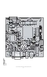
1/1
2-
2. P
O
WE
R S
U
PP
L
Y
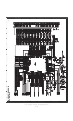
PW
B


