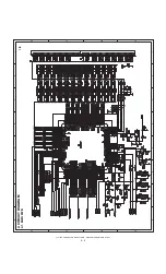
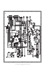
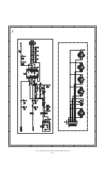
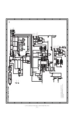
background image

LL-T15S3

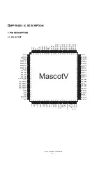
APPENDIX : IC DESCRIPTION

6 – 2

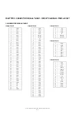
1-2. PIN DESCRIPTION
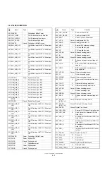
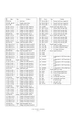
Pin 

No.

Name

Type

Definition

001 DIBVDD

Digital Input Buffer Power

002 CAP_HREF

I

Port B Horizontal Active Qualifier

003 CAP_HSYNC

I

Port B Horizontal Sync Input

004 CAP_VSYNC

I

Port B Vertical Sync Input

005 DIBVSS

Ground Digital Input Buffer Ground

006 BLU_INB_0/Y0

I

Port B Blue Input Bit 0/YUV Data Input 
Y0

007 BLU_INB_1/Y1

I

Port B Blue Input Bit 1/YUV Data Input 
Y1

008 BLU_INB_2/Y2

I

Port B Blue Input Bit 2/YUV Data Input 
Y2

009 BLU_INB_3/Y3

I

Port B Blue Input Bit 3/YUV Data Input 
Y3

010 BLU_INB_4/Y4

I

Port B Blue Input Bit 4/YUV Data Input 
Y4

011 BLU_INB_5/Y5

I

Port B Blue Input Bit 5/YUV Data Input 
Y5

012 BLU_INB_6/Y6

I

Port B Blue Input Bit 6/YUV Data Input 
Y6

013 BLU_INB_7/Y7

I

Port B Blue Input Bit 7/YUV Data Input 
Y7

014 DCVDD

Power Digital Core Power

015 GRN_INB_0

I

Port B Green Input Bit 0

016 GRN_INB_1

I

Port B Green Input Bit 1

017 GRN_INB_2

I

Port B Green Input Bit 2

018 GRN_INB_3

I

Port B Green Input Bit 3

019 GRN_INB_4

I

Port B Green Input Bit 4

020 GRN_INB_5

I

Port B Green Input Bit 5

021 GRN_INB_6

I

Port B Green Input Bit 6

022 GRN_INB_7/

RTS0

I

Port B Green Input Bit 7

023 DCVSS

Ground Digital Core Ground

024 RED_INB_0/

UV0

I

Port B Red Input Bit 0/YUV Data Input 
UV0

025 RED_INB_1/

UV1

I

Port B Red Input Bit 1/YUV Data Input 
UV1

026 RED_INB_2/

UV2

I

Port B Red Input Bit 2/YUV Data Input 
UV2

027 RED_INB_3/

UV3

I

Port B Red Input Bit 3/YUV Data Input 
UV3

028 RED_INB_4/

UV4

I

Port B Red Input Bit 4/YUV Data Input 
UV4

029 RED_INB_5/

UV5

I

Port B Red Input Bit 5/YUV Data Input 
UV5

030 RED_INB_6/

UV6

I

Port B Red Input Bit 6/YUV Data Input 
UV6

031 RED_INB_7/

UV7

I

Port B Red Input Bit 7/YUV Data Input 
UV7

032 DIBVDD

Power Digital Input Buffer Power

033 DVDD

Power Digital VDD

034 DVSS

Ground Digital ground

035 DTEST

O

Digital test output

036 VCCD

Power Digital power

037 DGND

Ground Digital ground

038 VGA_VSYNC

I

Port A vertical SYNC

039 VGA_HSYNC

I

Port A horizontal SYNC

040 SOGI

I

Port A Sync-On-Green input

041 VCCA

Power Analog power for PLL

042 AGND

Ground Analog ground for PLL

043 VREF

I

External 25V reference voltage

044 CP

I

PLL loop filter for pole

045 CZ

I

PLL loop filter for zero

046 VCCAB

Power B channel analog power

047 BI

I

B channel analog input

048 GNDAB

Ground B channel analog ground

049 BCLP

O

B channel internal clamp voltage out-
put

050 VTOP

O

ADC resistor ladder top decoupling 
capacitor

051 VBOT

O

ADC resistor ladder bottom decou-
pling capacitor

052 VCCAG

Power G channel analog power

053 GI

I

G channel analog input

054 GNDAG

Ground G channel analog ground

055 GCLP

O

G channel internal clamp voltage out-
put

056 TOUTP

O

Differential testing output plus

057 TOUTM

O

Differential testing output minus

058 VCCAR

Power R channel analog power

059 RI

I

R channel analog input

060 RNDAR

Ground R channel analog ground

061 RCLP

O

R channel internal clamp voltage out-
put

062 ADVDD

(VDD_PLL)

Power Display PLL Analog Power

063 ADVSS

(VSS_PLL)

Ground Display PLL Analog Ground

064 DCVSS

Ground Digital Core Ground

065 OSD_FSW

I

External OSD Window Display Enable

066 OSD_CLK

O

Clock Output For External OSD Con-
troller Chip

067 OSD_R

I

R Data Input From External OSD Con-
troller Chip

068 OSD_G

I

G Data Input From External OSD Con-
troller Chip

069 OSD_B

I

B Data Input From External OSD Con-
troller Chip

070 OSD_I

I

Intensity Input From Ext OSD Control-
ler Chip

071 DCVDD

Power Digital Core Power

072 Reserved

R

Reserved

073 XTAL

O

Crystal Out

074 XTALI

I

Crystal Input

075 DIBVSS

Ground Digital Input Buffer Ground

076 DISP_DE

O

Display Enable

077 DISP_VSYNC

O

Display Vertical Sync

Pin 

No.

Name

Type

Definition

Summary of Contents for LL-T15S3

Page 1: ...cument has been published to be used for after sales service only The contents are subject to change without notice LLT15S3SME LCD MONITOR MODEL LL T15S3 CHAPTER 1 OUTLINE OF THE PRODUCT NOMENCLATURE AND FUNCTION 1 1 CHAPTER 2 CONNECTION ADJUSTMENT OPERATION AND FUNCTIONS 2 1 CHAPTER 3 DISASSEMBLY AND ASSEMBLY 3 1 CHAPTER 4 TROUBLESHOOTING 4 1 CHAPTER 5 CONNECTOR SIGNAL TABLE CIRCUIT DIAGRAM PWB L...

Page 2: ...Temperature of operating environment 5 35 C Power consumption 33W With no audio input 36W maximum 2W when in power saving mode Dimensions 338 W x 145 D x 313 H mm Weight Approx 3 9kg approx 3 3kg excluding stand Excluding analog signal cable DIMENSIONS UNITS MM Analog signal cable Approx 1 8m Audio cable Approx 1 8m SIGNAL TIMINGS Recommended resolution is 1024 x 768 All are compliant only with no...

Page 3: ...close the OSD On Screen Display Menu 2 c MODE button When the OSD Menu is displayed This button is used to select menu options When the OSD Menu is not displayed This button is used to set COLOR MODE 3 e d buttons When the OSD Menu is displayed These buttons are used to select an option or adjust the value of the selected option When the OSD Menu is not displayed These buttons are used to adjust b...

Page 4: ...arder in the middle of travel Continue raising by applying more force at that point Raise the display section until it stops when titled forward approx 5 2 Adjust to an easy to view angle 2 Angle adjustment Press down on the stand and adjust it to a suitable viewing angle Do not use the monitor when tilted back beyond approximately 25 The monitor may fall over leading to injury or malfunction 3 Fo...

Page 5: ...sory audio cable is connected to the audio output termi nal of the computer the sound of the connected computer is output from the monitor speakers You can also use the headphone jack of the display 1 2 CONNECTION OF HEADPHONES COMMERCIALLY AVAILABLE Headphones commercially available can be connected Note When the headphones are connected no sound can be heard from the monitor speakers 1 3 CONNECT...

Page 6: ...could lead to malfunction 5 Being careful not to damage the monitor spread out a soft cloth and lay the monitor on it display side down 6 Attach the arm to the monitor with four screws Note The screws used to attach the arm should be M4 screws with a length of 8 mm 10 mm protruding from the surface to be attached Using different screws could cause the monitor to fall off or to be internally damage...

Page 7: ... Power ON Power ON Press the above two buttons at same time and while turn the power on 2 ADJUSTMENT menu reset Press the two buttons at same time 3 Adjustment lock function While pressing the MENU button turn the power on 6 Screen adjustment MENU ADJUSTMENT AUTO CLOCK PHASE H POS V POS AUTO MENU GAIN CONTROL BLACK LEVEL CONTRAST MENU COOL STD WHITE BALANCE WARM USER R CONTRAST CONTRAST R G B G CO...

Page 8: ...redder than standard WARM Color tone redder than standard USER R CONTRAST e button for blue green d button for red G CONTRAST e button for purple d button for green B CONTRAST e button for yellow d button for blue MENU 4 MODE SELECT OSD H POSITION OSD horizontal position The position of the OSD display can be moved to the left and right e d buttons OSD V POSITION OSD vertical position The position...

Page 9: ...R SUPPLY INVERTER BOARD AND MAIN BOARD 1 Remove the hex screws A and screws B and then remove the shield 2 Remove the screws A and then remove the ground lead 3 Remove the connectors and screws B and then remove the power supply inverter board 4 Remove the connector locking tape 5 Remove the connectors and screws and then remove the main board 4 REMOVING LCD MODULE 1 Remove the screws A and then r...

Page 10: ...gnal is not input Synchronizing signal is input to main PWB Replace RGB cable with a new one LED turns on in orange Check power input system 1 Power supply PWB Normal Connected properly 2 Blown out fuse F1 3 Check 5VX 3 3VX 3 3VA VDD VD and VLCD are output 4 LED Check LED for breakage Check the path between P5 and U6 Check the cable for disconnection Replace any defective unit 1 Power supply PWB 2...

Page 11: ...ons while turning on power switch Screen stays in black Screen stays in white Screen jitters or on screen characters flicker Abnormal color Check the following signals 1 Check if module control signal is output U1 2 Check if VLCD voltage is output normally Yes No Yes No Yes No CLOCK and PHASE can be adjusted Does abnormal area move on screen when BLACK LEVEL or CONT is changed after H POS or V POS...

Page 12: ... RO4 26 GND 27 RO3 28 RO2 29 RO1 30 RO0 31 GND 32 GND 33 N C 34 N C 35 N C 36 GND 1 GND 2 DCLK 3 GND 4 DE O 5 VSYNC 6 HSYNC 7 N C 8 GND 9 BE7 10 BE6 11 BE5 12 BE4 13 GND 14 BE3 15 BE2 16 BE1 17 BE0 18 GND 19 GE7 20 GE6 21 GE5 22 GE4 23 GND 24 GE3 25 GE2 26 GE1 27 GE0 28 GND 29 RE7 30 RE6 31 RE5 32 RE4 33 GND 34 RE3 35 RE2 36 RE1 37 RE0 38 VLCD 39 VLCD 40 GND 1 12V 2 GND 3 GND 4 5V 5 BRI_Min 6 INV_...

Page 13: ...LL T15S3 CONNECTOR SIGNAL TABLE CIRCUIT DIAGRAM PWB LAYOUT 5 2 A B C D 8 7 6 5 4 3 2 1 1 2 3 4 5 6 7 8 D C B A 1 4 2 CIRCUIT DIAGRAM 2 1 MAIN PWB ...

Page 14: ...LL T15S3 CONNECTOR SIGNAL TABLE CIRCUIT DIAGRAM PWB LAYOUT 5 3 A B C D 8 7 6 5 4 3 2 1 1 2 3 4 5 6 7 8 D C B A 2 4 ...

Page 15: ...LL T15S3 CONNECTOR SIGNAL TABLE CIRCUIT DIAGRAM PWB LAYOUT 5 4 A B C D 8 7 6 5 4 3 2 1 1 2 3 4 5 6 7 8 D C B A 3 4 ...

Page 16: ...LL T15S3 CONNECTOR SIGNAL TABLE CIRCUIT DIAGRAM PWB LAYOUT 5 5 A B C D 8 7 6 5 4 3 2 1 1 2 3 4 5 6 7 8 D C B A 4 4 ...

Page 17: ...0A100V 1 3 2 R35 422R 1 FB4 1 2 D5 LL4148 2 1 D14 RGP10D 2 1 R51 1 4W100 R20 0R FB3 1 2 R21 0R RT1 2A 4R P 5 mm R23 0R R24 0R C26 6 8nF C19 3 3nF 5 R12 1M 0805 C24 15P 3KV R89 220R 3W Y2 C20 XXXX ZD6 1 2W 16 2 2 1 Q14 2S C 1815 T2 19 2600 5 6 7 9 1 2 3 4 8 R59 13 3K D17 10A 60V 1 3 2 R17 18K CN4 SM02B BHSS 1 TB JST 1 2 CN1 1 2 3 D6 DAN217 1 3 2 R87 xxxx D15 1N 4148 2 1 R38 1 4W 750K D3 LL4148 2 1 ...

Page 18: ...LL T15S3 CONNECTOR SIGNAL TABLE CIRCUIT DIAGRAM PWB LAYOUT 5 7 3 PWB LAYOUT 3 1 MAIN PWB A side ...

Page 19: ...LL T15S3 CONNECTOR SIGNAL TABLE CIRCUIT DIAGRAM PWB LAYOUT 5 8 B side ...

Page 20: ...LL T15S3 CONNECTOR SIGNAL TABLE CIRCUIT DIAGRAM PWB LAYOUT 5 9 3 2 POWER SUPPLY PWB ...

Page 21: ...153 152 151 150 149 148 147 146 145 144 143 142 141 140 139 138 137 136 135 134 133 132 131 130 129 128 127 126 125 124 123 122 121 TVCLK IRQ SCS SDA SCL RST GPIO1 GPIO0 DCVSS CONFIG4 CONFIG3 CONFIG2 CONFIG1 CONFIG0 PWM0 PWM1 DCVDD LCD_VEE LCD_VDD LCD_VBL DCVSS RED_OUTB_7 RED_OUTB_6 RED_OUTB_5 RED_OUTB_4 DOBVDD RED_OUTB_3 RED_OUTB_2 RED_OUTB_1 RED_OUTB_0 DOBVSS GRN_OUTB_7 GRN_OUTB_6 GRN_OUTB_5 GRN...

Page 22: ...er Digital Input Buffer Power 033 DVDD Power Digital VDD 034 DVSS Ground Digital ground 035 DTEST O Digital test output 036 VCCD Power Digital power 037 DGND Ground Digital ground 038 VGA_VSYNC I Port A vertical SYNC 039 VGA_HSYNC I Port A horizontal SYNC 040 SOGI I Port A Sync On Green input 041 VCCA Power Analog power for PLL 042 AGND Ground Analog ground for PLL 043 VREF I External 25V referenc...

Page 23: ...LU_OUTB_4 O Display Port B Blue Output Bit 4 117 BLU_OUTB_5 O Display Port B Blue Output Bit 5 118 BLU_OUTB_6 O Display Port B Blue Output Bit 6 119 BLU_OUTB_7 O Display Port B Blue Output Bit 7 120 DOBVSS Ground Digital Output Buffer Ground 121 GRN_OUTB_0 O Display Port B Green Output Bit 0 122 GRN_OUTB_1 O Display Port B Green Output Bit 1 123 GRN_OUTB_2 O Display Port B Green Output Bit 2 124 G...

Page 24: ...ace OSC REFCLK LCD Panel RED GREEN BLUE VSYNC HSYNC XSYNC SCL SDA CHROMA LUMINANCE COMPOSITE PA0 PA15 CAP_HS CAP_VS TVCLK IRQ RESET 24 EVEN DATA 24 ODD DATA PCLK DISP_EN HS VS VDD VBL VEE VDD Control VBL Control VEE Control OSD I OSD B OSD R OSD G OSD FSW OSD CLK HS VS Capture Interface LCD Power Switching Control OSD MASCOT SOG DCVDD DCVSS DOBVDD DOBVSS ...

Page 25: ...3 February Printed in Japan t COPYRIGHT 2003 BY SHARP CORPORATION All rights reserved Printed in Japan No part of this publication may be reproduced stored in a retrieval system or transmitted In any form or by any means electronic mechanical photocopying recording or otherwise without prior written permission of the publisher ...

Reviews: