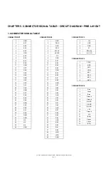
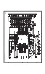
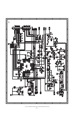

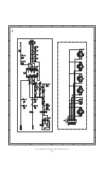
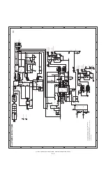


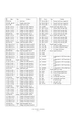

LL-T15S3
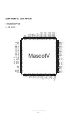
APPENDIX : IC DESCRIPTION
6 – 3
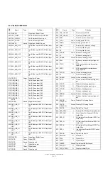
078 SHCLK
O
Shift Clock
079 DISP_HSYNC
O
Display Horizontal Sync
080 DCVSS
Ground Digital Core Ground
081 BLU_OUTA_0
O
Display Port A Blue Output Bit 0
082 BLU_OUTA_1
O
Display Port A Blue Output Bit 1
083 BLU_OUTA_2
O
Display Port A Blue Output Bit 2
084 BLU_OUTA_3
O
Display Port A Blue Output Bit 3
085 DOBVDD
Power Digital Output Buffer Power
086 BLU_OUTA_4
O
Display Port A Blue Output Bit 4
087 BLU_OUTA_5
O
Display Port A Blue Output Bit 5
088 BLU_OUTA_6
O
Display Port A Blue Output Bit 6
089 BLU_OUTA_7
O
Display Port A Blue Output Bit 7
090 DOBVSS
Ground Digital Output Buffer Ground
091 GRN_OUTA_0
O
Display Port A Green Output Bit 0
092 GRN_OUTA_1
O
Display Port A Green Output Bit 1
093 GRN_OUTA_2
O
Display Port A Green Output Bit 2
094 GRN_OUTA_3
O
Display Port A Green Output Bit 3
095 DOBVDD
Power Digital Output Buffer Power
096 GRN_OUTA_4
O
Display Port A Green Output Bit 4
097 GRN_OUTA_5
O
Display Port A Green Output Bit 5
098 GRN_OUTA_6
O
Display Port A Green Output Bit 6
099 GRN_OUTA_7
O
Display Port A Green Output Bit 7
100 DCVSS
Ground Digital Core Ground
101 RED_OUTA_0
O
Display Port A Red Output Bit 0
102 RED_OUTA_1
O
Display Port A Red Output Bit 1
103 RED_OUTA_2
O
Display Port A Red Output Bit 2
104 RED_OUTA_3
O
Display Port A Red Output Bit 3
105 DCVDD
Power Digital Core Power
106 RED_OUTA_4
O
Display Port A Red Output Bit 4
107 RED_OUTA_5
O
Display Port A Red Output Bit 5
108 RED_OUTA_6
O
Display Port A Red Output Bit 6
109 RED_OUTA_7
O
Display Port A Red Output Bit 7
110 DOBVSS
Power Digital Output Buffer Ground
111 BLU_OUTB_0
O
Display Port B Blue Output Bit 0
112 BLU_OUTB_1
O
Display Port B Blue Output Bit 1
113 BLU_OUTB_2
O
Display Port B Blue Output Bit 2
114 BLU_OUTB_3
O
Display Port B Blue Output Bit 3
115 DOBVDD
Power Digital Output Buffer Power
116 BLU_OUTB_4
O
Display Port B Blue Output Bit 4
117 BLU_OUTB_5
O
Display Port B Blue Output Bit 5
118 BLU_OUTB_6
O
Display Port B Blue Output Bit 6
119 BLU_OUTB_7
O
Display Port B Blue Output Bit 7
120 DOBVSS
Ground Digital Output Buffer Ground
121 GRN_OUTB_0
O
Display Port B Green Output Bit 0
122 GRN_OUTB_1
O
Display Port B Green Output Bit 1
123 GRN_OUTB_2
O
Display Port B Green Output Bit 2
124 GRN_OUTB_3
O
Display Port B Green Output Bit 3
125 DOBVDD
Power Digital Output Buffer Power
126 GRN_OUTB_4
O
Display Port B Green Output Bit 4
Pin
No.
Name
Type
Definition
127 GRN_OUTB_5
O
Display Port B Green Output Bit 5
128 GRN_OUTB_6
O
Display Port B Green Output Bit 6
129 GRN_OUTB_7
O
Display Port B Green Output Bit 7
130 DOBVSS
Ground Digital Output Buffer Ground
131 RED_OUTB_0
O
Display Port B Red Output Bit 0
132 RED_OUTB_1
O
Display Port B Red Output Bit 1
133 RED_OUTB_2
O
Display Port B Red Output Bit 2
134 RED_OUTB_3
O
Display Port B Red Output Bit 3
135 DOBVDD
Power Digital Output Buffer Power
136 RED_OUTB_4
O
Display Port B Red Output Bit 4
137 RED_OUTB_5
O
Display Port B Red Output Bit 5
138 RED_OUTB_6
O
Display Port B Red Output Bit 6
139 RED_OUTB_7
O
Display Port B Red Output Bit 7
140 DCVSS
Ground Digital Core Ground
141 LCD_VBL
O
LCD Panel VBL Backlight Control
142 LCD_VDD
O
LCD Panel VDD Source Control
143 LCD_VEE
O
LCD Panel VEE Control
144 DCVDD
Power Digital Core Power
145 PWM1
146 PWM0
147 CONFIG0
I
Configuration Pin 0 (I2C Slave Address
Bit 0)
148 CONFIG1
I
Configuration Pin 1 (I2C Slave Address
Bit 1)
149 CONFIG2
I
Configuration Pin 2 (I2C Slave Address
Bit 2)
150 CONFIG3
I
Configuration Pin 3 (I2C Slave Address
Bit 3)
151 CONFIG4
I
Configuration Pin 3 (Serial Bus Select)
152 DCVSS
Ground Digital Core Ground
153 GPI00
I/O
General Purpose Input/Output
154 GPI01
I/O
General Purpose Input/Output
155 RST
I
System Reset
156 SCL
I/O
Host Interface Serial Clock
157 SDA
I/O
Host Interface Serial Data
158 SCS#
I
Serial Chip Select
159 IRQ#
O
Interrupt To Host
160 TVCLK
I
Port B Clock Input
Pin
No.
Name
Type
Definition